Andreev spectroscopy of the triplet superconductivity state in Bi/Ni bilayer system
Abstract
We calculate the Andreev spectroscopy between a ferromagnetic lead and a Bi/Ni bilayer system. The bilayer system is described by Anderson-Brinkman-Morel(ABM) state and mixing ABM and -wave state. In both the ABM state and the mixed ABM state and -wave state, the Andreev conductance is consistent with that obtained in the point contact experiment[Zhao,et al, arXiv:1810.10403]. Moreover, the conductance peak near the zero energy is induced by the surface state of the ABM phase. Our work may provides helpful clarification for understanding of recent experiments.
I Introduction
Triplet -wave superconductors have received much interestTinkham (2004) which provide new insights into topological superfluidityVollhardt et al. (1991); Mizushima et al. (2016), superconductivity, and new spintronics applicationsRomeo and Citro (2013); Nayak et al. (2008). Especially, topological -wave superconductorsHasan and Kane (2010); Qi et al. (2009); Delaire et al. (2010); Sato (2009); Ryu et al. (2010) promise quantum computing applications such as Majorana fermions which locate at the edges and the vortex cores of superconductorsRead and Green (2000); Ivanov (2001); Volovik (2009a, b); Roy (2010); Das Sarma et al. (2006). Topological -wave superfluid of have been reportedMurakawa et al. (2009) and superconductivity in has been suggestedKashiwaya et al. (2011, 2014). Another peculiar feature of topological materials is the gapless surface statesThouless et al. (1982); Halperin (1982); Tanaka et al. (2012); Kashiwaya et al. (2014). Experimentally, the surface state can be detected by the Andreev spectroscopyKashiwaya et al. (1995a); Kashiwaya and Tanaka (2000); Kashiwaya et al. (2014).
Recent point contact experiments have observed triplet superconductivity in epitaxial Bi/Ni bilayersMoodera and Meservey (1990); Kumar et al. (2011); Siva et al. (2015); Gong et al. (2015); Liu et al. (2018); Zhao et al. (2018); Chao (2019). Triplet p-wave superconductivity was inferred from the zero-bias peak of the Andreev conductance between the epitaxial Bi/Ni bilayer and the ferromagnetic metal. Furthermore, a quantitative analysis of the Andreev conductance revealed a triplet -wave Anderson-Brinkman-Morel (ABM) stateAnderson and Morel (1960); Anderson and Brinkman (1973), with two Weyl nodes. In contrast, the recent time-domain THz spectroscopy experimentChauhan et al. (2019) have reported a nodeless bulk superconductivity in the epitaxial Bi/Ni bilayer. In addition, the inversion symmetry of the Bi/Ni bilayer is broken, suggesting the mixing of different pairings such as -wave and -waveSato and Ando (2017); Bauer and Sigrist (2012). The Bi/Ni bilayer system naturally raises two questions: (1)Does the broken inversion symmetry admit any superconducting paring other than the ABM state at the interface? (2) Given the importance of the behavior of surface states in topological superconductors, how do those surface states and bulk ABM states contribute to the transport properties?
We build a model that calculates the Andreev spectroscopy and local density of states of superconducting materials i.e. the ABM state and the ABM state mixture with -wave pairing. We first calculate the conductance of the Andreev reflection in pure ABM state using the Blonder-Tinkham-Klapwijk (BTK) methodBlonder et al. (1982); Bauer and Sigrist (2012), and its local density of states by the surface Green’s function methodPeng et al. (2017); Umerski (1997); Sancho et al. (1985). Second, we calculate the Andreev conductance of the ABM state mixture with -wave superconductivity. The Andreev conductance of both the pure ABM state and the mixed state with a small -wave component were consistent with the results of point contact experimentsZhao et al. (2018). However, in mixed states with a large -wave component, the conductance deviated from the point contact resultsZhao et al. (2018). After computing the local density of states of those state, we find nodes in the pure ABM state and the mixed state with small -wave component, but not in the mixed state with large -wave component. The local density of states of mixed state with large -wave component is consistent with the time-domain THz spectroscopy experimentChauhan et al. (2019). We also revealed that the conductance peak near the zero energy is contributed by the surface state.
The remainder of this paper is organized as follows.
Section II, introduces our model for calculating the conductance.
Section III, and IV, calculate the conductances and the surface statestates of the ABM state and an unconventional superconductivity state(an ABM state mixed with a -wave state), respectively. The paper concludes with a brief summary.
II Model
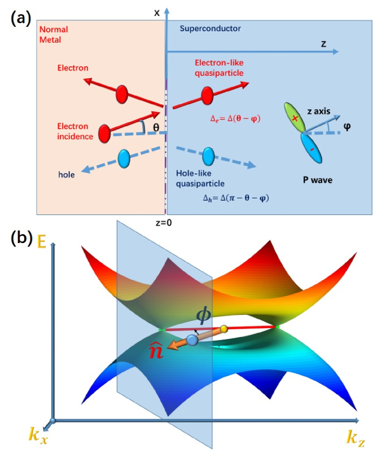
Consider a normal metal-superconductor (N-S) junction located at z = 0( where z 0 represents the superconductor, and z0 represents normal metal) as shown in Fig. 1(a). Here, we only consider the case of incident on the x-z plane, because the pairing function is isotropic on the x-y plane for the ABM state.
The effective Hamiltonian in the Nambu representation is given byBauer and Sigrist (2012):
| (1) |
where , , for singlet pairing and for triplet pairingBauer and Sigrist (2012).
We first consider the superconducting order parameter of of a p-wave superconductor in the pure ABM stateAnderson and Morel (1960); Anderson and Brinkman (1973):
| (2) |
where with being the Fermi momentum and being the component of . According to BTK theoryBlonder et al. (1982); Bauer and Sigrist (2012), the wavefunction of a superconductor is given by:
| (3) |
where , . Here, denotes the electron(hole) like state for spin index , and denotes the electron(hole) like state for spin index , , , , , with . Here, , with , and denote the effective pair potentials of electron-like and hole-like quasiparticles, respectivelyTanaka and Kashiwaya (1995); Bauer and Sigrist (2012); Zhao et al. (2018), where depicts the electron incident angle and represents the angle between the x axis of the -wave and the normal to the interface (similar to the angle between the x axis of the d wave the interface normal in a d-wave superconductorTanaka and Kashiwaya (1995)), as shown in Fig . 1(b).
Second, we consider a mixed -wave pairing and ABM state, whose superconducting order parameter has the following form: Bauer and Sigrist (2012); Frigeri et al. (2004). Then, the superconducting order parameters split into two independent order parameters and respectivelyIniotakis et al. (2007). In this case, the wave function changes to , , and . Here, and have the same form as the former case, with , .
The wavefunction in the lead region is derived from the Hamiltonian: ; where , and denote the kinetic energy and the chemical potential respectively. The plane wave at the normal metal side can be expressed by a four-component wavefunction in the Nambu representation :
| (4) |
The first row of Fq.4 describes an electron with a spin up incident plane wave and a normal reflection wave. The second row describes an electron with a spin down wave. The third row and the fourth row are hole descriptors with a spin-up and a spin-down Andreev reflection wave, respectively. The in normal metal(NM) lead, and in ferromagnetic metal(FM) leadChen et al. (2012) describe the evanescent wave. Note that we only consider the incidence of spin-up electrons. Fully polarized ferromagnetic lead, contain only spin-up electrons whereas in nonmagnetic lead, the spin-up and spin-down electrons are identical, so it is sufficient to consider spin-up electrons only.
Next, we study the transport properties of the N/S junction. We assume that the N/S interface located at z=0 along the x axis has an infinitely narrow insulating barrier described by the delta function Yokoyama et al. (2005); Bauer and Sigrist (2012); Zhao et al. (2018). Solving the following boundary conditionsYokoyama et al. (2005); Bauer and Sigrist (2012); Zhao et al. (2018)
| (5) |
we obtain and . The normalized conductance with a bias voltage isZhao et al. (2018):
| (6) |
where , and , , the parameter represents the energy broadeningChen et al. (2012).
III The conductance and surface state of ABM state
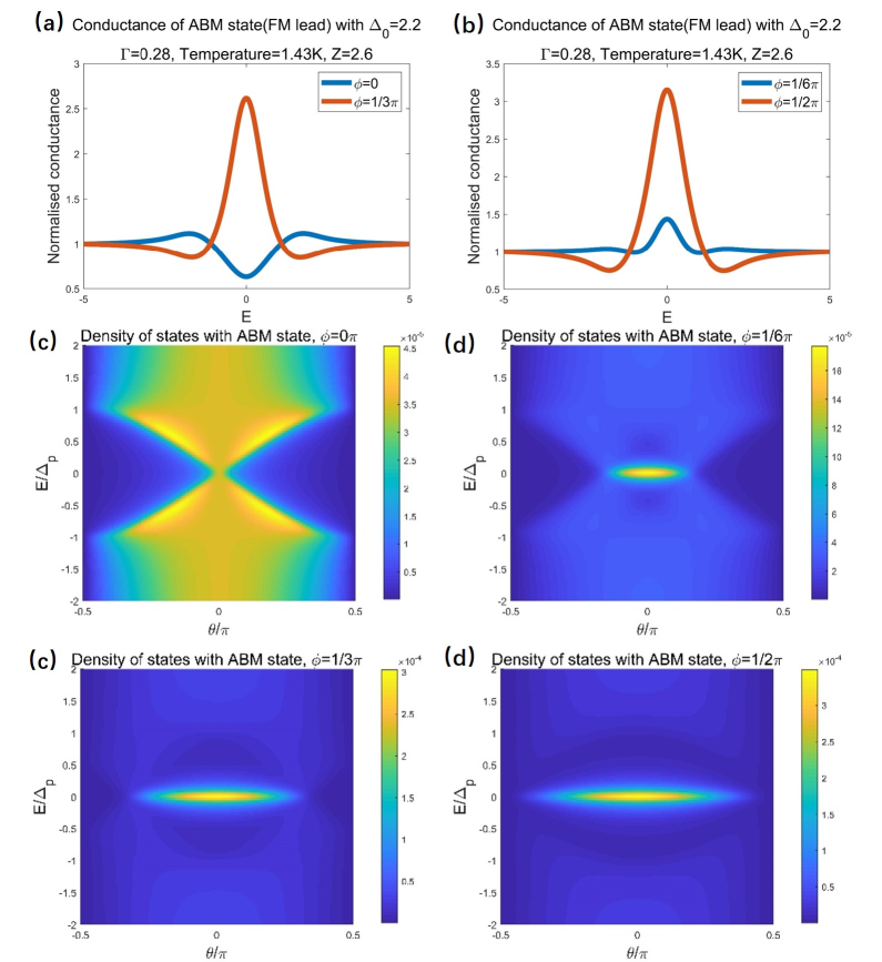
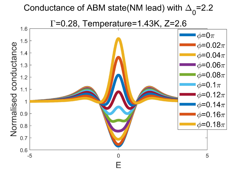
We first calculated the normalized Andreev conductance between ferromagnetic/non-magnetic lead and ABM state at different incident planes, denoted by . The interface parameters were obtained by fitting the conductance to the experimental results on the c plane. In subsequent analysis, we mainly set is equal to and because the results of approximated the experimental results of the c plane. Detail information about experimental fitting procedure is detailed in the Appendix.
As shown in Fig 2(a) and (b), the conductance near the zero energy changed from a valley to a peak as increase. At is zero, the conductivity near the zero energy was valley shaped. Increasing the , gradually increases the conductance at zero energy, and the conductance peak.
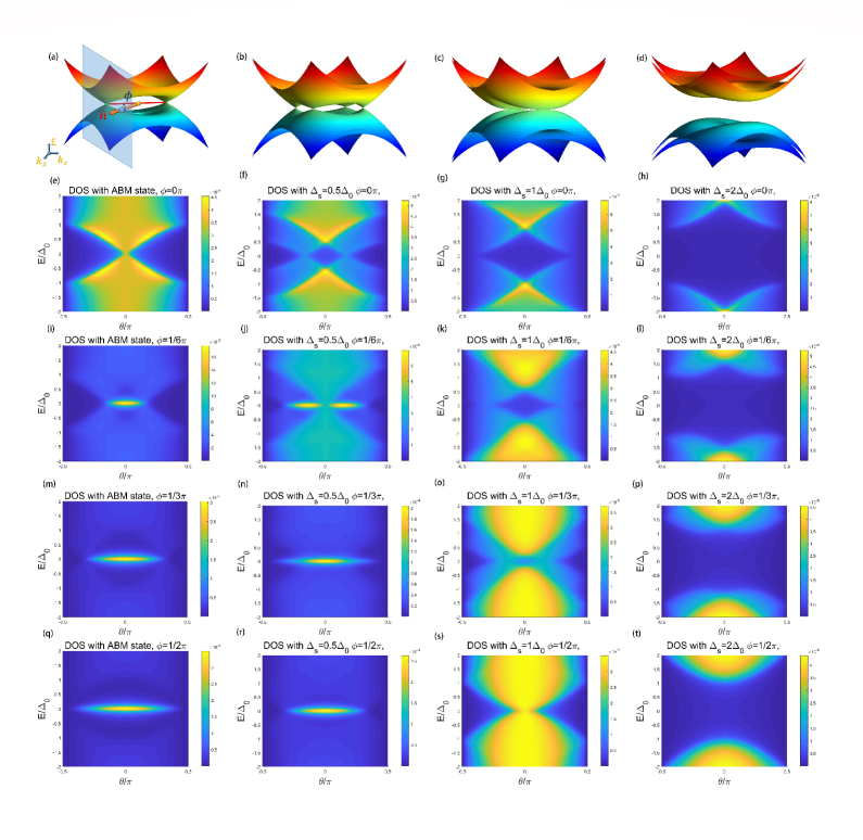
Comparing the density of states localized on the surface with the energy band of the ABM state, we observe that the conductivity at the zero energy is contributed by the projection of the surface state between the two Weyl points on the incident plane at the zero energy. First, as the local density of states on the surface was consistent with the conductivity spectrum, the conductance could be attributed to the strength of the density of states. At [Fig 2(c)], the density of states exhibited a funnel-like shape, forming a valley of conductance. As increased [Fig 2(d)-(f)], the density of states became increasingly concentrated around the zero energy, leading to a more pronounced peak in the conductance spectrum. However, as shown in Fig 1(b), the band structure of the ABM state was similar to that of Weyl semimetals, with only two Weyl points at zero energy. Previous work has reported a Fermi arc between the two Weyl pointsSu-Yang et al. (2015); Jia et al. (2016). Comparing the density of states with the band structure, we inferred that the zero energy state is the projection of the Fermi arc on the incident plane.
Conductance spectroscopy of the Andreev reflection between ferromagnetic/non-magnetic lead and the ABM state at different incident planes was consistent with the density of states. Both the density of states and the conductance spectrum are given in the appendix.
IV mixture of ABM state and -wave state
The -wave and -wave states can mix in the Bi/Ni bilayer because the inversion symmetry brokenSato and Ando (2017); Bauer and Sigrist (2012). We next studied the Andreev reflection of unconventional superconductors composed of the ABM state and -wave superconductors.
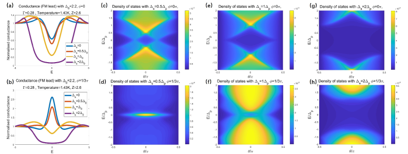
The Andreev conductance was qualitatively consistent with that of the pure ABM state when [Fig 3(a) and (b)], but with that of the pure -wave state when . As the conductivity at zero energy is mainly contributed by the zero energy surface state, we next investigated the effect of the -wave component on the surface state.
As -wave component increased, the surface and bulk states near the zero energy gradually weakened and eventually disappeared [Fig 3(c) (h)]. When , the -wave component split the funnel-like formation of the previous density of states into two parts: a left and a right part. As the -wave component increased, the split widened and the two nodes at zero energy gradually move apart and disappeared, thereby reducing the zero-energy conductance. The splitting increased the density of states in the overlapping parts of the two nodes. Increasing the -wave component, also shifted the higher density region from the zero energy, increasing the conductance valley width. However, at , as the -wave component increased from 0 to the -wave component, the surface state weakened and disappeared. When the -wave component exceeded the -wave component, it split the density of states into two parts. Further increases of the -wave component gradually increased the distance between the two parts and diminished the conductance at zero energy, widening the conductance valley. Moreover, in this case, the -wave component more severely affected the conductance in FM lead than conductance in NM lead.
In summary, the -wave component reduced the surface state and the conductance at zero energy. When the -wave component was less than the -wave component, the conductance profile resembled that of the pure ABM state and also matched the experimental resultsZhao et al. (2018). The energy band retained it zero-energy nodes in this case. However, when the S-wave component exceeded the p-wave component, the conductance profile formed a shape of the valley and the energy band formed a globe gap. Therefore, when the -wave component was small, the conductance was qualitatively consistent with the point contact resultsZhao et al. (2018) but the energy band failed to explain the time-domain THz spectroscopyChauhan et al. (2019). In contrast, when the S-wave component was large, the energy band was consistent with the time-domain THz spectroscopyChauhan et al. (2019) but the conductance failed to explain the point contact resultsZhao et al. (2018).
V Summary
We studied the Andreev reflection conductance between ferromagnetic lead and two types of superconductors (a pure ABM state superconductor and a mixed state ABM state and -wave state) by the BTK function method. First, we found that the conductance of the pure ABM state is consistent with that of point contact experimentsZhao et al. (2018). Second, the result of the mixed state with a small -wave component was qualitatively consistent with that of the pure ABM state and the point contact experimentsZhao et al. (2018). However,when the -wave component was large, the conductance deviated from the point resultsZhao et al. (2018) because the gap opened and widened in the energy band. We also calculated the local density of states, and attributed the conductance peak at zero energy to the surface state of the ABM state component. Our work provides some complementary explanations for the results of recent experiments.
VI Acknowledgments
This work is supported by the National Natural Science Foundation of China (No.11674028, No.61774017, No.11734004 and No.21421003) and National Key Research and Development Program of China(Grant No. 2017YFA0303300).
References
- Tinkham (2004) M. Tinkham, Introduction to Superconductivity, 2nd ed., Dover Books on Physics (Courier Corporation, Dover, 2004).
- Vollhardt et al. (1991) D. Vollhardt, P. Wolfle, and R. B. Hallock, Physics Today 44, 60 (1991).
- Mizushima et al. (2016) T. Mizushima, Y. Tsutsumi, T. Kawakami, M. Sato, M. Ichioka, and K. Machida, Journal of the Physical Society of Japan 85, 022001 (2016), https://doi.org/10.7566/JPSJ.85.022001 .
- Romeo and Citro (2013) F. Romeo and R. Citro, Phys. Rev. Lett. 111, 226801 (2013).
- Nayak et al. (2008) C. Nayak, S. H. Simon, A. Stern, M. Freedman, and S. Das Sarma, Rev. Mod. Phys. 80, 1083 (2008).
- Hasan and Kane (2010) M. Z. Hasan and C. L. Kane, Rev. Mod. Phys. 82, 3045 (2010).
- Qi et al. (2009) X.-L. Qi, T. L. Hughes, S. Raghu, and S.-C. Zhang, Phys. Rev. Lett. 102, 187001 (2009).
- Delaire et al. (2010) O. Delaire, M. S. Lucas, A. M. dos Santos, A. Subedi, A. S. Sefat, M. A. McGuire, L. Mauger, J. A. Muñoz, C. A. Tulk, Y. Xiao, M. Somayazulu, J. Y. Zhao, W. Sturhahn, E. E. Alp, D. J. Singh, B. C. Sales, D. Mandrus, and T. Egami, Phys. Rev. B 81, 094504 (2010).
- Sato (2009) M. Sato, Phys. Rev. B 79, 214526 (2009).
- Ryu et al. (2010) S. Ryu, A. P. Schnyder, A. Furusaki, and A. W. W. Ludwig, New Journal of Physics 12, 065010 (2010).
- Read and Green (2000) N. Read and D. Green, Phys. Rev. B 61, 10267 (2000).
- Ivanov (2001) D. A. Ivanov, Phys. Rev. Lett. 86, 268 (2001).
- Volovik (2009a) G. E. Volovik, JETP Letters 90, 587 (2009a).
- Volovik (2009b) G. E. Volovik, JETP Letters 90, 398 (2009b).
- Roy (2010) R. Roy, Phys. Rev. Lett. 105, 186401 (2010).
- Das Sarma et al. (2006) S. Das Sarma, C. Nayak, and S. Tewari, Phys. Rev. B 73, 220502 (2006).
- Murakawa et al. (2009) S. Murakawa, Y. Tamura, Y. Wada, M. Wasai, M. Saitoh, Y. Aoki, R. Nomura, Y. Okuda, Y. Nagato, M. Yamamoto, S. Higashitani, and K. Nagai, Phys. Rev. Lett. 103, 155301 (2009).
- Kashiwaya et al. (2011) S. Kashiwaya, H. Kashiwaya, H. Kambara, T. Furuta, H. Yaguchi, Y. Tanaka, and Y. Maeno, Phys. Rev. Lett. 107, 077003 (2011).
- Kashiwaya et al. (2014) S. Kashiwaya, H. Kashiwaya, K. Saitoh, Y. Mawatari, and Y. Tanaka, Physica E: Low-dimensional Systems and Nanostructures 55, 25 (2014), topological Objects.
- Thouless et al. (1982) D. J. Thouless, M. Kohmoto, M. P. Nightingale, and M. den Nijs, Phys. Rev. Lett. 49, 405 (1982).
- Halperin (1982) B. I. Halperin, Phys. Rev. B 25, 2185 (1982).
- Tanaka et al. (2012) Y. Tanaka, M. Sato, and N. Nagaosa, Journal of the Physical Society of Japan 81, 011013 (2012), https://doi.org/10.1143/JPSJ.81.011013 .
- Kashiwaya et al. (1995a) S. Kashiwaya, Y. Tanaka, M. Koyanagi, H. Takashima, and K. Kajimura, Phys. Rev. B 51, 1350 (1995a).
- Kashiwaya and Tanaka (2000) S. Kashiwaya and Y. Tanaka, Reports on Progress in Physics 63, 1641 (2000).
- Moodera and Meservey (1990) J. Moodera and R. Meservey, Physical Review B 42, 179 (1990).
- Kumar et al. (2011) J. Kumar, A. Kumar, A. Vajpayee, B. Gahtori, D. Sharma, P. Ahluwalia, S. Auluck, and V. Awana, Superconductor Science and Technology 24, 085002 (2011).
- Siva et al. (2015) V. Siva, K. Senapati, B. Satpati, S. Prusty, D. Avasthi, D. Kanjilal, and P. K. Sahoo, Journal of Applied Physics 117, 083902 (2015).
- Gong et al. (2015) X.-X. Gong, H.-X. Zhou, P.-C. Xu, D. Yue, K. Zhu, X.-F. Jin, H. Tian, G.-J. Zhao, and T.-Y. Chen, Chinese Physics Letters 32, 067402 (2015).
- Liu et al. (2018) L. Liu, Y. Xing, I. Merino, H. Micklitz, D. Franceschini, E. Baggio-Saitovitch, D. Bell, and I. Solórzano, Physical Review Materials 2, 014601 (2018).
- Zhao et al. (2018) G. Zhao, X. Gong, J. He, J. Gifford, H. Zhou, Y. Chen, X. Jin, C. Chien, and T. Chen, arXiv preprint arXiv:1810.10403 (2018).
- Chao (2019) S.-P. Chao, Phys. Rev. B 99, 064504 (2019).
- Anderson and Morel (1960) P. W. Anderson and P. Morel, Phys. Rev. Lett. 5, 136 (1960).
- Anderson and Brinkman (1973) P. W. Anderson and W. F. Brinkman, Phys. Rev. Lett. 30, 1108 (1973).
- Chauhan et al. (2019) P. Chauhan, F. Mahmood, D. Yue, P.-C. Xu, X. Jin, and N. Armitage, Physical review letters 122, 017002 (2019).
- Sato and Ando (2017) M. Sato and Y. Ando, Reports on Progress in Physics 80, 076501 (2017).
- Bauer and Sigrist (2012) E. Bauer and M. Sigrist, Non-centrosymmetric superconductors: introduction and overview, Vol. 847 (Springer Science & Business Media, 2012).
- Blonder et al. (1982) G. Blonder, M. Tinkham, and T. Klapwijk, Physical Review B 25, 4515 (1982).
- Peng et al. (2017) Y. Peng, Y. Bao, and F. von Oppen, Phys. Rev. B 95, 235143 (2017).
- Umerski (1997) A. Umerski, Phys. Rev. B 55, 5266 (1997).
- Sancho et al. (1985) M. P. L. Sancho, J. M. L. Sancho, J. M. L. Sancho, and J. Rubio, Journal of Physics F: Metal Physics 15, 851 (1985).
- Tanaka and Kashiwaya (1995) Y. Tanaka and S. Kashiwaya, Phys. Rev. Lett. 74, 3451 (1995).
- Frigeri et al. (2004) P. A. Frigeri, D. F. Agterberg, A. Koga, and M. Sigrist, Phys. Rev. Lett. 92, 097001 (2004).
- Iniotakis et al. (2007) C. Iniotakis, N. Hayashi, Y. Sawa, T. Yokoyama, U. May, Y. Tanaka, and M. Sigrist, Phys. Rev. B 76, 012501 (2007).
- Kashiwaya et al. (1995b) S. Kashiwaya, Y. Tanaka, M. Koyanagi, H. Takashima, and K. Kajimura, Journal of Physics and Chemistry of Solids 56, 1721 (1995b).
- Chen et al. (2012) T. Y. Chen, Z. Tesanovic, and C. L. Chien, Phys. Rev. Lett. 109, 146602 (2012).
- Yokoyama et al. (2005) T. Yokoyama, Y. Tanaka, and J. Inoue, Physical Review B 72, 220504 (2005).
- Su-Yang et al. (2015) X. Su-Yang, B. Ilya, A. Nasser, N. Madhab, B. Guang, Z. Chenglong, S. Raman, C. Guoqing, Y. Zhujun, and L. Chi-Cheng, Science 349, 613 (2015).
- Jia et al. (2016) S. Jia, S. Y. Xu, and M. Z. Hasan, Nature Materials 15, 1140 (2016).
- Sancho et al. (1984) M. P. L. Sancho, J. M. L. Sancho, and J. Rubio, Journal of Physics F: Metal Physics 14, 1205 (1984).
VII appendix A: surface green function
Here, we briefly introduce the method of calculating the surface Green’s functionSancho et al. (1984). First, we discretize the Hamiltonian along the z direction and label each layer with its corresponding z value (layer i=1 n). Then, the Hamiltonian is given by:
| (7) |
where denotes the coupling between the i and i’ layer. After discretizing the Hamiltonian, the surface Green’s function is obtained by the following procedure:
First define the parameters:
| (8) |
Second, iterate the expressions until ,
| (9) |
Third. define The surface Green’s function is :. From this function, we obtain the density of states on the the superconductor surface.
VIII appendix B: Fitting of the experimental results
Using our model developed in Section II we fited the experimentally obtained normalized Andreev reflection conductances in FM and NM lead (see Fig 4 ). The fittings were obtained different incident surfaces with different interface parameters and different .
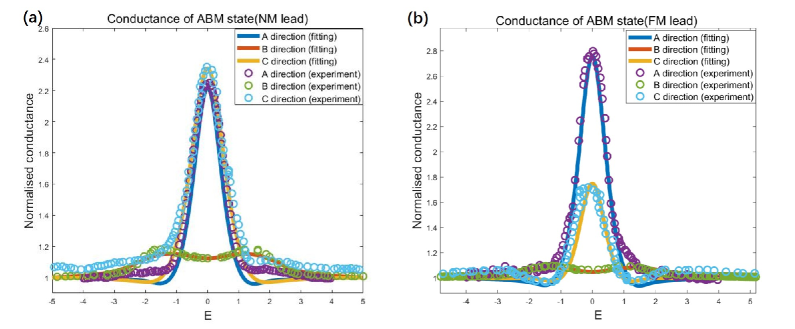
For the results of NM lead, the parameters were set as follows: in the a plane, in the b plane, and in the c plane. For the results of FM lead, the parameters were set to: in the a plane, in the b plane, and in the c plane.
IX appendix C: The conductance with different incidence plane
Using our model, we calculated the normalized the Andreev reflection conductance for different incidence planes of NM lead. The results are plotted in Fig 5. The conductance varied slowly with changes in the incident plane.
X appendix D: influence of -wave component on energy band, conductance and surface states
We first calculated the density of states for different -wave components and incident planes. The S-wave exerted a huge influence on the energy band and density of states, splitting both original energy band [Fig 6(a)-(d)] and the original hourglass profile [Fig 6(e)-(g)] into two parts.
As shown in Fig 6(i)-(k), (m)-(o) and (q)-(s), the -wave component also decreased the surface density of states. At , the surface states disappeared completely.
Moreover, the -wave component created a growing gap in both the energy band and density of states for different incident planes [Fig 6(c)and(d), (k)and(l), (o)and(p), (s)and(t)].
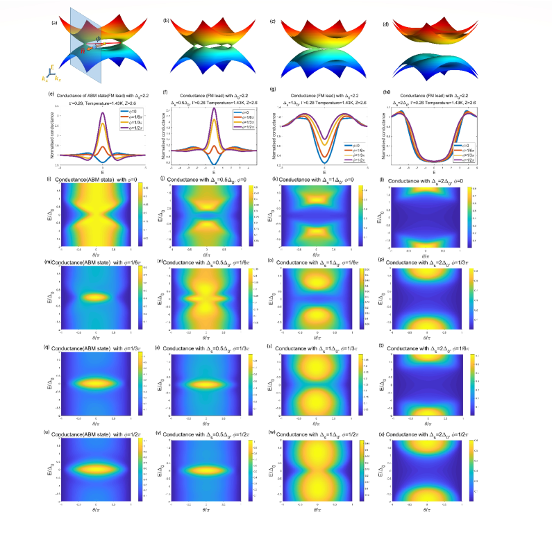
Second, we calculated the influence of the -wave component on the conductance for different incident planes between the FM lead and superconductor. As shown in Fig 7(e)-(h), the -wave component decreased the conductance near the zero energy. When , the conductance profile resembled that of Andreev conductance in the pure ABM state; when , it was similar to the Andreev conductance in a pure -wave superconductor.
The influence of the -wave component on the conductance spectrum for different incident planes is shown in Fig 7(e)-(x). The conductance spectrum resembled that of the local density of states. When and was non-zero, the -wave component decreased the conductance near the zero energy by decreasing the surface density of states near the zero energy. However, when and , it decreased the conductance near the zero energy by splitting the density of states. Finally, when , it decreased the conductance far from the zero energy by expanding the gap between the high density of states regions.
Note that the conductance spectra and densities of states are consistent at very small energy expansions ().
Next, we calculated the influence of the -wave component on the conductance for different incident planes between NM lead and superconductor. The conductance and its spectrum were different in magnitude but qualitatively consistent with those of FM lead in the same situations.