Large spatial extension of the zero-energy Yu-Shiba-Rusinov state in magnetic field
Abstract
Various promising qubit concepts have been put forward recently based on engineered superconductor (SC) subgap states like Andreev bound states, Majorana zero modes or the Yu-Shiba-Rusinov (Shiba) states. The coupling of these subgap states via a SC strongly depends on their spatial extension and is an essential next step for future quantum technologies. Here we investigate the spatial extension of a Shiba state in a semiconductor quantum dot coupled to a SC for the first time. With detailed transport measurements and numerical renormalization group calculations we find a remarkable more than 50 nm extension of the zero energy Shiba state, much larger than the one observed in very recent scanning tunneling microscopy (STM) measurements. Moreover, we demonstrate that its spatial extension increases substantially in magnetic field.
Superconductor nanostructures are the most advanced platforms for quantum computational architectures thanks to the macroscopic coherent wavefunction and the robust protection by the superconducting gap. Recently, various novel qubit concepts like the Andreev (spin) qubits Padurariu and Nazarov (2012); Janvier et al. (2015); Park and Yeyati (2017); Hays et al. (2018); Tosi et al. (2019), Majorana box qubits Leijnse and Flensberg (2012a); Aasen et al. (2016); Aguado (2017), braiding with Majorana zero modes in a Majorana or a Shiba-chain Sau and Sarma (2012); Choy et al. (2011); Nadj-Perge et al. (2013); Braunecker and Simon (2013); Pientka et al. (2013); Klinovaja et al. (2013); Nakosai et al. (2013); Vazifeh and Franz (2013); Kim et al. (2014); Nadj-Perge et al. (2014) have been put forward or even implemented. All these qubits are based on their associated sub-gap states such as Andreev bound states Beenakker and van Houten (1991), Majorana zero modes Sau et al. (2010); Alicea (2010); Lutchyn et al. (2010); Oreg et al. (2010); Leijnse and Flensberg (2012b); Mourik et al. (2012); Nadj-Perge et al. (2014); Deng et al. (2016) or Shiba states Luh (1965); Shiba (1968); Rusinov (1969); Balatsky et al. (2006). The Shiba state is formed when a magnetic adatom or its artificial version (quantum dot) is coupled to a superconductor and the localized magnetic moment creates a subgap state by binding an anti-aligned quasiparticle from the superconductor. Depending on the coupling strength between the superconductor and the magnetic moment, the ground state can be either the screened local moment with singlet character, or the unscreened doublet states, .
The coupling of these sub-gap states via a superconductor is an essential next step towards 2-qubit operations or state engineering, e.g. an Andreev molecule Pillet et al. (2018); Scherb̈l et al. (2019); Kornich et al. (2019) or a Majorana-chain, which consists of series of adatoms or quantum dots interlinked by the superconductor Sau and Sarma (2012); Choy et al. (2011); Nadj-Perge et al. (2013); Braunecker and Simon (2013); Pientka et al. (2013); Klinovaja et al. (2013); Nakosai et al. (2013); Vazifeh and Franz (2013); Kim et al. (2014); Nadj-Perge et al. (2014); Kim et al. (2018); Steinbrecher et al. (2018); Kamlapure et al. (2018). Obviously, the coupling between such sub-gap states strongly depends on their spatial extension into the superconductor, so it is required for these localized states to extend as much as possible.
So far, the spatial extent and structure of the Shiba states was investigated by STM measurements on magnetic adatoms deposited on the surface of a superconductor Ji et al. (2008); Choi et al. (2017); Ménard et al. (2015); Ruby et al. (2016) and, interestingly, it revealed that the dimensionality plays a crucial role Ménard et al. (2015). In a three dimensional isotropic s-wave superconductor, it was found that the Shiba states decay over a very short distance of the order of nm Ji et al. (2008); Choi et al. (2017), but extends one order of magnitude further, as far as nm, if the impurity is placed on the surface of a two-dimensional superconductor Ménard et al. (2015, 2017).
In this work, we investigate the spatial extension of the Shiba state formed when an artificial atom is strongly coupled to a superconductor. The Shiba state is observed at a remarkably large distance of more than 50 nm. Furthermore, for the first time we explore the effect of an external magnetic field on the extension of the Shiba state, as it is relevant to access topological superconducting states. Remarkably, with increasing magnetic field, the spatial extension increases significantly further.
Shiba states were widely studied in two different types of systems: a) in STM measurements, when magnetic particles are deposited on the surface of a superconductor Yazdani et al. (1997); Ji et al. (2008); Hatter et al. (2015); Ménard et al. (2015); Ruby et al. (2016); Choi et al. (2017); Kezilebieke et al. ; Cornils et al. (2017); Ménard et al. (2017); Farinacci et al. (2018); Heinrich et al. (2018); Schneider et al. , and b) in nanocircuits, when a quantum dot is attached to the superconductor Buitelaar et al. (2002); Eichler et al. (2007); Sand-Jespersen et al. (2007); Deacon et al. (2010a, b); Dirks et al. (2011); Kim et al. (2013); Pillet et al. (2010); Chang et al. (2013); Pillet et al. (2013); Kumar et al. (2014); Schindele et al. (2014); Lee et al. (2014); Jellinggaard et al. (2016); Lee et al. (2017); Gramich et al. (2017); Li et al. (2017); Bretheau et al. (2017); Su et al. (2017, 2018, 2019). The STM geometry allows for the spatial mapping of the Shiba state Ji et al. (2008); Choi et al. (2017); Ménard et al. (2015); Ruby et al. (2016), but the strength of the coupling between the magnetic adatom and the substrate is mostly determined by the microscopic details and its tuning remains quite challenging Hatter et al. (2015); Farinacci et al. (2018). In contrast, the quantum dot realization enables the tuning the energy of the Shiba state via the level position or the tunnel couplings by using external gate voltages Lee et al. (2014); Jellinggaard et al. (2016). Another advantage of the latter setup is the potential to apply an external magnetic field without stability issues.
Results
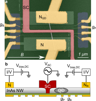
Implementation of the Shiba device. In this paper, we implement a combined approach of systems a) and b), where a tunnel probe is attached to a superconductor–quantum dot hybrid. The schematics of the used device are shown on Fig. 1a. A quantum dot (QD in gray) is strongly coupled to a superconductor (SC in red), leading to the formation of a Shiba state. An additional tunnel electrode (N in yellow) is coupled weakly to the superconductor at a fixed distance from the dot. Applying a small bias between SC and N, the tunnel current, and the corresponding differential conductance, are measured, while the energy of the Shiba state is tuned by the plunger gate .
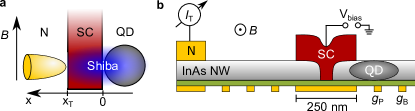
The device is implemented in an InAs semiconducting nanowire (gray), contacted by a 250 nm wide Pb superconducting electrode in the middle (SC in red), and one normal contact (N in yellow) on the left side (see Fig. 1b). The electron density in the nanowire is tuned by an array of gates fabricated below the nanowire. The nanowire was cut by focused ion beam (FIB) prior to the deposition of the superconducting contact to suppress the direct tunnel coupling between the two arms Fülöp et al. (2014, 2015). The width of the FIB cut is about nm. The quantum dot is formed in the right arm of the wire and its level position is tuned by the voltage on the plunger gate . The tunnel coupling to the right side can be turned on and off by the barrier gate . Although not displayed in Fig. 1, there is a normal electrode to the right of , which allows us to measure direct transport through the quantum dot (see Methods). The bulk coherence length for Pb is about nm, however, in e-beam evaporated layers the elastic mean free path is considerably reduced Morris and Tinkham (1961), limiting the coherence length to nm. An in-plane magnetic field is applied perpendicular to the nanowire axis. Further details on the fabrication and the experimental techniques are presented in the Methods.
Observation of the Shiba state in the tunnel current. First we present the results of transport measurements for the strongly coupled superconductor – quantum dot setup isolated from the rest of the device on the right by . The differential conductance of the tunnel probe, is shown in Fig. 2 as function of and for different values of the magnetic field. In the absence of magnetic field (see panel a), two pairs of resonances with enhanced conductance are present on top of a smooth conductance background of about (with the conductance quantum). The conductance increment along the lines is about . We use the plunger gate voltage to tune the level position and subsequently the charge on the quantum dot, while the barrier gate voltage is used to isolate the dot from the rest of the nanowire on its right side. The barrier gate has a cross capacitance to the dot, resulting a tilt of the otherwise horizontal resonances. As we explain below, the enhanced conductance lines are the signatures of the zero-energy Shiba state. The presence of the current enhancement is striking, since in usual STM setups the Shiba wavefunction is observed only up to a distance of 10 nm. On the contrary, we observe the Shiba state more than 50 nm away from the quantum dot.
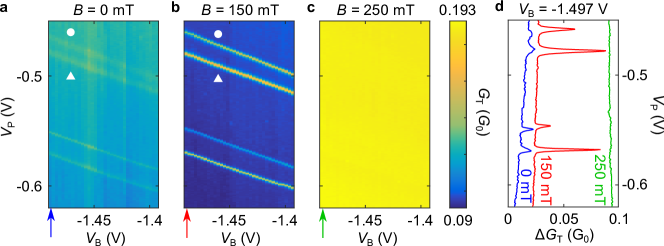
Remarkably, applying a magnetic field smaller than the critical field, the conductance enhancement significantly increases (see Fig. 2b, being measured in 150 mT). The largest conductance peak we observe is of size , approximately 20 times larger than the zero magnetic field value.
In a 250 mT magnetic field, above the critical field of the superconductor, mT, the resonances vanish (see Fig. 2c), indicating that the origin of the signal is related to superconductivity. To further illustrate the strong dependence of the signal on the magnetic field, we present in panel c line cuts at a fixed V for the same magnetic fields as in the other panels.
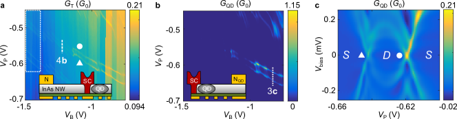
In the following, let us understand what condition of the quantum dot is linked to the tunnel current enhancement. As discussed in the Methods, our device is equipped with an extra normal electrode NQD on the right of the quantum dot, which previously was isolated from the rest of the device by the large negative voltage. Increasing to more positive values opens up the barrier to N, which allows for a direct transport characterization of the quantum dot. In this way, we were able to measure in parallel both the differential conductance through the quantum dot itself, , and the conductance through the tunnel probe, . Figs. 3a and b show the conductance of the tunnel probe and the quantum dot, respectively, in a larger gate voltage window in the absence of an external magnetic field. The region marked by a white dotted rectangle is the particular voltage window in Fig. 2a. Let us follow the resonances (marked by circle and triangle) in the plot of the tunnel current as increases.
For V the tunnel barrier becomes sufficiently small, and transport through the quantum dot also sets in (see panel b of Fig. 3). The similarities between the resonances in and those in indicate that the two conductances are related; the tunnel conductance enhancement is linked to the level position of the quantum dot, i.e. the enhancement is observed when the dot is on resonance with the Fermi level of the superconductor.
To gain further insight to the level structure of the quantum dot, a finite bias measurement was performed along the white dashed line on Fig. 3b, at V. The results are shown in Fig. 3c. The eye-shaped crossing of the sub-gap conductance lines are the usual fingerprints of the Shiba state (see e.g. Ref. Eichler et al. (2007)). The results presented in Fig. 3 show that there is strong coupling between superconductor and quantum dot. In the previously shown measurements of Figs. 2, 3a and 3b, the enhanced conductance lines correspond to the Shiba state when its energy is tuned to zero by . These resonances (marked by white triangle and circle) correspond to the singlet-doublet and doublet-singlet transitions of the Shiba state. Since the position of the enhancement lines coincides with these transitions, we conclude that – even in the case of large tunnel barriers when the quantum dot is coupled only to the superconductor (i.e. for V) – the conductance enhancement takes place when the energy of the Shiba state is tuned to zero. These results provide direct evidence that the tunneling electrode N indeed probes the Shiba state, and implies that the Shiba state extends in real space over the distance between the dot and the tunnel probe, separated by an impressive distance of nm. Here the width of the FIB cut gives the lower and the entire width of the superconducting lead the upper bound (see Fig. 1b).
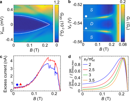
Further increased extension in magnetic field. A detailed analysis of the finite magnetic field behavior is presented on Fig. 4. Panel a shows the reduction of the superconducting gap, with the magnetic field measured on the quantum dot. The gap smoothly decreases in magnetic field and continuously vanishes at mT, the critical field. The white dashed line is a fit, discussed below.
The detailed evolution of the tunnel current enhancement with the magnetic field – measured along the dashed line in Fig. 3a at V – is shown on Fig. 4b. While close to , the peaks are barely visible, they are strongly enhanced with increasing magnetic field, particularly between 100 and 200 mT. For higher field values the peaks decrease and they disappear above .
Discussion
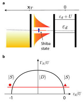
To explain the magnetic field dependence of the conductance enhancement and to probe the spatial extension of the Shiba state, we have set up a theoretical framework that allows us to compute the tunneling current though the normal lead N in a N–SC–QD geometry in a non-perturbative fashion. We assume that the quantum dot is coupled to the superconductor at , while the normal lead is contacted to the superconductor further away at a coordinate . Moreover, we consider that the tunnel probe acts as an STM tip and measures the local density of states by injecting electrons at . Electrons entering the superconductor propagate to the quantum dot, scatter on it, and propagate back to be extracted at a later time but at the same position (The model is detailed in the Methods).
For a practical calculation, we need to determine the -matrix that describes the scattering of the conduction electrons on the artificial atom. In our model, this is related to the Green’s function of the creation operators on the quantum dot, as first discussed by Langreth Langreth (1966). Close to the parity changing transition and close to zero bias, the quasiparticles’ contribution is irrelevant, and only the subgap states contribute. Using field theoretical methods, we computed the total current flowing from the normal lead through the Shiba state by performing a numerical renormalization group (NRG) calculation.
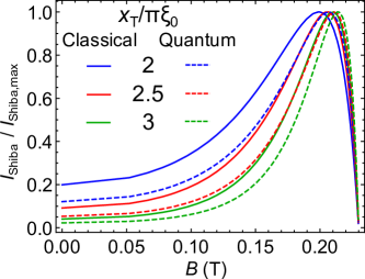
Fig. 4c and d compare the experimental and NRG results as a function of magnetic field. In panel c the spectral weight for the experimental data is evaluated along the two dashed lines in panel b. The independent conductance background was subtracted from , and the excess tunnel conductance was integrated for the enhancement peaks (marked by circle and triangle) to get the total excess current/spectral weight induced by the Shiba state. The NRG-computed excess currents (see Eq. (12) of Methods) are displayed for different ratios of and in panel d, and show a close resemblance to the experimentally observed field dependence. For both panels and for low magnetic fields, the excess current strongly increases with the magnetic field, has a maximum, and linearly decreases at higher fields to vanish at the critical field, mT.
In order to understand this field dependence, it is instructive to display the results obtained for a classical spin on the dot (see Methods). This minimal model captures most of the experimentally observed features and it is in good agreement with the NRG results (see Methods). In the classical case, the current carried by the Shiba state at the transition reads
| (1) |
Here stands for the dimensionless conductance of the N–SC contact in the normal state (in units of ), and denote the electron and hole parts of the bound Shiba state’s wave function, and is the density of states in the superconductor. The amplitude can be easily computed for a spherical Fermi surface, yielding
| (2) |
with a geometry, position, and spatial dimension dependent dimensionless amplitude, and the superconducting coherence length with the Fermi velocity.
Apparently, the magnetic field dependence of the gap and thus that of the correlation length, , is mostly responsible for the unusual magnetic field dependence observed in our experiment. In the framework of Ginzburg-Landau theory, the order parameter in an external magnetic field is given by , where is the zero-field gap, the magnetic field, and stands for the critical magnetic field at which superconductivity vanishes. Experimentally, however, we find a slightly different functional form for the suppression, qualitatively similar to that observed in thin films Morris and Tinkham (1961); Anthore et al. (2003) (dashed line on Fig. 4a), as
| (3) |
with eV and mT. For , Eq. (3) together with Eq. (2) implies an exponential increase in the current with increasing magnetic field and then a suppression close to due to the prefactor . This is consistent with the upturn of measured current enhancement at low fields, below mT (see Fig. 4c), and its suppression close to the critical field. According to Eq. (2), the current should be maximal for . Using mT – where the total excess current is maximal (see Fig. 4c) – this condition yields to . However note that the theory slightly overestimates the magnetic field value where the excess current is maximal – and so underestimates the ratio of . This deviance may originate from the fact that our model idealizes the setup, i.e. neglects the presence of quasiparticles and a possibly finite subgap density of states. Keeping this deviance in mind, the obtained ratio is still roughly consistent with our geometrical parameters, the separation of the quantum dot and the normal electrodes , and a reduced coherence length, , compatible with a diffusive superconductor.
Let us turn to differences compared to typical STM measurements of Shiba states: In STM characterization of the Shiba wavefunction, is significantly weaker. Moreover, it oscillates upon varying the tip-adatom distance, , and becomes unobservable at distances larger than 10 nm for 3D superconductors. These characteristic differences originate in the quite different geometries used in our setup and in STM experiments.
In STM measurements, the amplitude is responsible for the spatial oscillations. It has a modulation of , which originates in the point-like nature of the tunnel probe Balatsky et al. (2006); Ménard et al. (2015), and the fact that one usually tunnels either to the electron- or hole-like states with amplitudes and , respectively. In contrary, in our setup, two effects seem to eliminate these oscillations. First, the N–SC interface has a large tunnel surface ( where is the nanowire diameter, nm), and averaging for different distances and tunneling paths is expected to eliminate oscillations both in distance (not accessible in our setup) as well as in the field dependence Bouchiat (2005). Second, at the transition point the electron and hole-like contributions add up and, surprisingly, the the combination does not contain any oscillating term in any dimension. This indicates that interference effects probably play little role right at the transition, where our measurements are carried out.
In an STM geometry is a small signal (pA) Ménard et al. (2015), while in our measurement, it can reach values as large as (at the excitation of V), even though the normal electrode is at a separation nm away from the quantum dot. According to Eq. (2), is directly proportional to . The small for typical STM experiments is a result of two factors: the weak tunnel coupling and also the fast, decay of in a 3D superconductor. In our case, is relatively large, in the range of . Additionally, the N–SC tunneling area is very large, , compensating the decay of , in close resemblance to lower dimensional superconductors. A combination of these effects can explain how the Shiba state can be observed even from a remote position, significantly larger than the one in STM measurements Ji et al. (2008); Choi et al. (2017); Ménard et al. (2015); Ruby et al. (2016). In our quantum dot based setup, the observation distance is determined essentially only by the coherence length of the superconductor, and the coupling between Shiba states hosted around quantum dots can be achieved at significantly larger distances than in case of adatoms.
Finally let us contrast our findings with the results of Cooper pair splitter measurements, where two quantum dots are attached to both sides of the superconductor, and contrary to our setup, current flows from the superconductor through both quantum dots towards the normal leads. Current correlations between the two arms are induced by splitting up Cooper pairs Hofstetter et al. (2009); Herrmann et al. (2010); Hofstetter et al. (2011); Das et al. (2012); Schindele et al. (2012). There, electronic correlations extend over distances of about nm, comparable with the separation nm in our experiment. However, while the Shiba current, increases in a magnetic field, the Cooper pair splitting signal gets strongly suppressed Hofstetter (2011).
In conclusion we have studied the Shiba state in a SC–QD hybrid device by measuring the differential conductance in a tunnel probe attached to the superconductor at distance of nm away from the quantum dot. A large current enhancement has been observed when the Shiba resonance is tuned to zero energy. In an external magnetic field, the signal is further enhanced, implying an exponential growth for the extension of the Shiba state. The observed behavior is consistent with our microscopic theoretical model and field theoretical calculations. In our device, we can access the Shiba state from a remarkably large distance compared to previous experiments on magnetic impurities on superconducting substrates. These results establish an important milestone towards the realization of Shiba-chains implemented by a series of quantum dots attached to superconductors.
Acknowledgments
We acknowledge Morten H. Madsen for MBE growth, Jens Paaske, András Pályi, Dimitri Roditchev and Pascal Simon for useful discussions. We also acknowledge SNI NanoImaging Lab for FIB cutting.
This work was supported by the National Research Development and Innovation Office of Hungary within the Quantum Technology National Excellence Program 2017-1.2.1-NKP-2017-00001, by the New National Excellence Program of the Ministry of Human Capacities, by QuantERA SuperTop project 127900, by AndQC FetOpen project, by Nanocohybri COST Action CA16218, and by the Danish National Research Foundation. CPM was supported by the Romanian National Authority for Scientific Research and Innovation, UEFISCDI, under project no. PN-III-P4-ID-PCE-2016-0032. CS acknowledges support from the Swiss National Science Foundation through grant Nr. 20020L7263a and through the National Center of Competence in Research on Quantum Science and Technology (QSIT).
Author contributions:
Experiments were designed by C. S. and S. C., wires were developed by J. N., devices were developed and fabricated by G. F. and J. G., measurements were carried out and analyzed by Z. S., G. F., A. B., P. M., T. E. and S. C. Theoretical analysis was given by C. P. M. and G. Z.. And Z. S., C. P. M., G. Z. and S. C. prepared the manuscript.
Additional information: The authors declare no competing interests. Correspondence should be addressed to S. C..
Methods
Sample fabrication and measurement details.
An SEM micrograph of the measured device is shown in Fig. 5. First, 9 bottom gate electrodes were defined by electron beam lithography and evaporation of 4 nm Ti and 18 nm Pt. Two m wide gates were used below the normal contacts and one, 250 nm wide below the superconductor. The remaining 3+3 bottom gates are 30 nm wide with 100 nm period. The gates were covered by 25 nm SiN, using plasma enhanced chemical vapor deposition, to serve as an insulating layer Fülöp et al. (2014). The SiN was removed at the end of bottom gate electrodes by reactive ion etching with CHF3/O2 Wong and Ingram (1992), to contact the gate electrodes. The InAs nanowire was deposited by micro-manipulator onto the SiN layer, approximately perpendicular to the bottom gates. The NWs were grown by gold catalyst assisted MBE growth Aagesen et al. (2007); Madsen et al. (2013), using a two-step growth method to suppress the stacking faults Shtrikman et al. (2009). The normal (N and N), Ti/Au (4.5/100 nm) and superconducting (SC), Pd/Pb/In (4.5/110/20 nm) contact were defined in further e-beam lithography and evaporation steps Gramich et al. (2016). The later has a width of 250 nm. Prior to the evaporation, the nanowire was passivated in ammonium sulfide solution to remove the native oxide from the surface Suyatin et al. (2007).
Prior to the deposition of the superconducting contact the nanowire was cut by FIB to prevent direct tunneling between the NW segment, which can lead to spurious effects Fülöp et al. (2014, 2015). The width of the FIB cut was about 50 nm, giving a lower bound for the distance of the quantum dot and the tunnel probe.
The measurements were done in a Leiden Cryogenics CF-400 top loading cryo-free dilution refrigerator equipped with a 9+3 T 2D vector-magnet. The measurements were done at a bath temperature of 35 mK. Prior to the cool down, the sample was pumped overnight to remove the adsorbed water contamination from the surface of the nanowire. The currents were measured by standard lock-in technique at 237 Hz. The AC signal of V was applied to the superconducting electrode. The currents in the left and right arm were measured simultaneously via the two normal leads by home-built I/V converters. The DC bias was applied symmetrically to the normal leads. An in-plane magnetic field was applied parallel to the superconducting electrode, perpendicular to the nanowire. The circuit diagram is shown in Fig. 5b. In most of the measurements presented in the main text, N was electrically isolated from the rest of the device by applying a large negative voltage on gate .
Shiba bound state and the parity crossing transition.
We model the superconductor using the s-wave BCS theory Schrieffer (1964)
| (4) |
where is the creation operator of a spin and momentum and is the superconducting order parameter, which can be considered real.
The QD can be described by means of the Anderson model,
| (5) |
with is the single particle energy and is the on-site Coulomb energy. The operator here creates an electron with spin on the dot, and . In our geometry the dot is located at the position and is tunnel-coupled to the superconductor (See Fig. 6a), as described by the Hamiltonian
| (6) |
The factor , normalized to one at the Fermi surface, , accounts for the directional dependence of the tunneling, and prefers tunneling directions perpendicular to the SC–QD interface in our geometry.
In the local moment regime, we can neglect charge fluctuations of the dot, and describe it in terms of a simple Kondo model,
| (7) |
with , and the exchange coupling to the spin of the quantum dot, .
This latter Hamiltonian can be solved exactly in the classical limit Shiba (1968), where one finds a subgap resonance at an energy:
| (8) |
where , and stands for the standard dimensionless Kondo coupling. With increasing coupling strength the bound state energy eventually crosses zero, and the impurity binds to itself a quasiparticle of opposite spin direction.
Although this classical calculation captures the parity changing transition, determines its location incorrectly. In reality, the phase transition originates from the competition between the superconducting correlations and the Kondo screening of the spin, and the transition takes place when , with a characteristic Fermi liquid temperature scale. Deep in the local moment regime, can be identified as the Kondo temperature, , but it becomes of the order of the tunneling rate between the dot and the superconductor close to the mixed valence regime. For , the spin of the dot remains unscreened down to zero temperature, resulting in a doublet ground state ={} and a first excited singlet state, , the so-called Shiba state inside the gap. By increasing the tunneling rate , the spin in the QD binds a quasiparticle from the superconductor, and becomes the ground state. The corresponding qualitative phase diagram is displayed in Fig. 6b.
In the experiments, changing the voltage corresponds to moving along the red horizontal line in the phase diagram. At the intersections with the ”dome” (denoted by the circle and the triangle), the Shiba state is at zero energy, and is in resonance with the Fermi energy, of the tunneling electrode N, leading to the observed sudden increase in the zero voltage differential conductance.
Tunnel conductance and current.
In our setup, the normal lead acts as an STM tip measuring the differential conductance across the device at a point away from the dot. In the small SC–N tunneling limit Andreev processes can be neglected, and tunneling from the normal electrode to the superconductor yields at temperature a current
| (9) |
at a finite voltage bias . Here denotes the density of states in the normal lead, is the tunneling amplitude between the superconductor and the normal contact, and is the energy dependent density of states in the superconductor at position . This latter can be expressed in terms of the Fourier transform of the retarded Green’s function, .
The Green’s function can be obtained by means of standard many-body theory, invoking Nambu spinors, , and corresponding propagators, . In this language, the quantum dot induced part of the propagator can be expressed as
| (10) |
Here describes the propagation of an electron (or hole) in the superconductor from the dot to the probe at an energy ,
| (11) |
with the Pauli matrices and acting in the Nambu space, while the -matrix describes scattering off the quantum dot.
We focus on transport through midgap states, i.e. . There the propagators are real, and the tunneling density of states is related to .
In the classical limit, we can determine analytically,
and extract the strength of its poles within the gap. At the transition points, , and expressing furthermore propagator we arrive at the equation (2) displayed in the main text.
In the framework of the Anderson model, we first introduce the spinors . Similar to Costi (2000), it is easy to show that the -matrix is directly related to the -levels’ Nambu propagator,
The subgap structure of is completely determined by the transition matrix elements and , and the energy difference of the singlet ground state and the many-body Shiba excitations, and , related by time reversal symmetry. At the transition point, the electron and hole contributions add up, and the expression of the tunnel current simplifies to
| (12) |
with , and the tunneling rate from the quantum dot to the superconductor. The results shown on Fig. 4d of the main text are generated by Eq. (12). Notice that the many-body expression differs from the classical one solely by the factor , which replaces the gap in the prefactor of the classical expression.
The matrix elements and can be directly extracted from NRG computations. A comparison between the two approaches is presented in Fig. 7. They both give similar results. Small quantitative differences are presumably due to the fact that the classical picture is not able to capture neither the mixed valence regime nor the proper Kondo scale, in contrast to the more elaborate NRG approach.
Data availability
The data that support the plots within this paper and other findings of this study are available at https://doi.org/10.5281/zenodo.3604194.
References
- Padurariu and Nazarov (2012) C. Padurariu and Y. V. Nazarov, EPL (Europhysics Letters) 100, 57006 (2012).
- Janvier et al. (2015) C. Janvier, L. Tosi, L. Bretheau, Ç. Ö. Girit, M. Stern, P. Bertet, P. Joyez, D. Vion, D. Esteve, M. F. Goffman, H. Pothier, and C. Urbina, Science 349, 1199 (2015), http://science.sciencemag.org/content/349/6253/1199.full.pdf .
- Park and Yeyati (2017) S. Park and A. L. Yeyati, Phys. Rev. B 96, 125416 (2017).
- Hays et al. (2018) M. Hays, G. de Lange, K. Serniak, D. J. van Woerkom, D. Bouman, P. Krogstrup, J. Nygård, A. Geresdi, and M. H. Devoret, Phys. Rev. Lett. 121, 047001 (2018).
- Tosi et al. (2019) L. Tosi, C. Metzger, M. F. Goffman, C. Urbina, H. Pothier, S. Park, A. L. Yeyati, J. Nygård, and P. Krogstrup, Phys. Rev. X 9, 011010 (2019).
- Leijnse and Flensberg (2012a) M. Leijnse and K. Flensberg, Semiconductor Science and Technology 27, 124003 (2012a).
- Aasen et al. (2016) D. Aasen, M. Hell, R. V. Mishmash, A. Higginbotham, J. Danon, M. Leijnse, T. S. Jespersen, J. A. Folk, C. M. Marcus, K. Flensberg, and J. Alicea, Phys. Rev. X 6, 031016 (2016).
- Aguado (2017) R. Aguado, La Rivista del Nuovo Cimento 40, 523 (2017).
- Sau and Sarma (2012) J. D. Sau and S. D. Sarma, Nature Communications 3, 964 (2012), article.
- Choy et al. (2011) T.-P. Choy, J. M. Edge, A. R. Akhmerov, and C. W. J. Beenakker, Phys. Rev. B 84, 195442 (2011).
- Nadj-Perge et al. (2013) S. Nadj-Perge, I. K. Drozdov, B. A. Bernevig, and A. Yazdani, Phys. Rev. B 88, 020407 (2013).
- Braunecker and Simon (2013) B. Braunecker and P. Simon, Phys. Rev. Lett. 111, 147202 (2013).
- Pientka et al. (2013) F. Pientka, L. I. Glazman, and F. von Oppen, Phys. Rev. B 88, 155420 (2013).
- Klinovaja et al. (2013) J. Klinovaja, P. Stano, A. Yazdani, and D. Loss, Phys. Rev. Lett. 111, 186805 (2013).
- Nakosai et al. (2013) S. Nakosai, Y. Tanaka, and N. Nagaosa, Phys. Rev. B 88, 180503 (2013).
- Vazifeh and Franz (2013) M. M. Vazifeh and M. Franz, Phys. Rev. Lett. 111, 206802 (2013).
- Kim et al. (2014) Y. Kim, M. Cheng, B. Bauer, R. M. Lutchyn, and S. Das Sarma, Phys. Rev. B 90, 060401 (2014).
- Nadj-Perge et al. (2014) S. Nadj-Perge, I. K. Drozdov, J. Li, H. Chen, S. Jeon, J. Seo, A. H. MacDonald, B. A. Bernevig, and A. Yazdani, Science 346, 602 (2014), https://science.sciencemag.org/content/346/6209/602.full.pdf .
- Beenakker and van Houten (1991) C. W. J. Beenakker and H. van Houten, Phys. Rev. Lett. 66, 3056 (1991).
- Sau et al. (2010) J. D. Sau, R. M. Lutchyn, S. Tewari, and S. Das Sarma, Phys. Rev. Lett. 104, 040502 (2010).
- Alicea (2010) J. Alicea, Phys. Rev. B 81, 125318 (2010).
- Lutchyn et al. (2010) R. M. Lutchyn, J. D. Sau, and S. Das Sarma, Phys. Rev. Lett. 105, 077001 (2010).
- Oreg et al. (2010) Y. Oreg, G. Refael, and F. von Oppen, Phys. Rev. Lett. 105, 177002 (2010).
- Leijnse and Flensberg (2012b) M. Leijnse and K. Flensberg, Phys. Rev. B 86, 134528 (2012b).
- Mourik et al. (2012) V. Mourik, K. Zuo, S. M. Frolov, S. R. Plissard, E. P. A. M. Bakkers, and L. P. Kouwenhoven, Science 336, 1003 (2012), http://www.sciencemag.org/content/336/6084/1003.full.pdf .
- Deng et al. (2016) M. T. Deng, S. Vaitiekenas, E. B. Hansen, J. Danon, M. Leijnse, K. Flensberg, J. Nygård, P. Krogstrup, and C. M. Marcus, Science 354, 1557 (2016), https://science.sciencemag.org/content/354/6319/1557.full.pdf .
- Luh (1965) Y. Luh, Acta Physica Sinica 21, 75 (1965).
- Shiba (1968) H. Shiba, Progress of Theoretical Physics 40, 435 (1968), /oup/backfile/content_public/journal/ptp/40/3/10.1143/ptp.40.435/2/40-3-435.pdf .
- Rusinov (1969) A. I. Rusinov, Soviet Journal of Experimental and Theoretical Physics 29, 1101 (1969).
- Balatsky et al. (2006) A. V. Balatsky, I. Vekhter, and J.-X. Zhu, Rev. Mod. Phys. 78, 373 (2006).
- Pillet et al. (2018) J. D. Pillet, V. Benzoni, J. Griesmar, J. L. Smirr, and . . Girit, “Non-local josephson effect in andreev molecules,” (2018), arXiv:1809.11011 .
- Scherb̈l et al. (2019) Z. Scherb̈l, A. Pályi, and S. Csonka, Beilstein J. Nanotechnology 10, 363 (2019).
- Kornich et al. (2019) V. Kornich, H. S. Barakov, and Y. V. Nazarov, “Fine energy splitting of overlapping andreev bound states in multi-terminal superconducting nanostructures,” (2019), arXiv:1906.06734 .
- Kim et al. (2018) H. Kim, A. Palacio-Morales, T. Posske, L. Rózsa, K. Palotás, L. Szunyogh, M. Thorwart, and R. Wiesendanger, Science Advances 4 (2018), 10.1126/sciadv.aar5251, https://advances.sciencemag.org/content/4/5/eaar5251.full.pdf .
- Steinbrecher et al. (2018) M. Steinbrecher, R. Rausch, K. T. That, J. Hermenau, A. A. Khajetoorians, M. Potthoff, R. Wiesendanger, and J. Wiebe, Nature Communications 9, 2853 (2018).
- Kamlapure et al. (2018) A. Kamlapure, L. Cornils, J. Wiebe, and R. Wiesendanger, Nature Communications 9, 3253 (2018).
- Ji et al. (2008) S.-H. Ji, T. Zhang, Y.-S. Fu, X. Chen, X.-C. Ma, J. Li, W.-H. Duan, J.-F. Jia, and Q.-K. Xue, Phys. Rev. Lett. 100, 226801 (2008).
- Choi et al. (2017) D.-J. Choi, C. Rubio-Verdú, J. de Bruijckere, M. M. Ugeda, N. Lorente, and J. I. Pascual, Nature Communications 8, 15175 EP (2017), article.
- Ménard et al. (2015) G. C. Ménard, S. Guissart, C. Brun, S. Pons, V. S. Stolyarov, F. Debontridder, M. V. Leclerc, E. Janod, L. Cario, D. Roditchev, P. Simon, and T. Cren, Nature Physics 11, 1013 (2015).
- Ruby et al. (2016) M. Ruby, Y. Peng, F. von Oppen, B. W. Heinrich, and K. J. Franke, Phys. Rev. Lett. 117, 186801 (2016).
- Ménard et al. (2017) G. C. Ménard, S. Guissart, C. Brun, R. T. Leriche, M. Trif, F. Debontridder, D. Demaille, D. Roditchev, P. Simon, and T. Cren, Nature Communications 8, 2040 (2017).
- Yazdani et al. (1997) A. Yazdani, B. A. Jones, C. P. Lutz, M. F. Crommie, and D. M. Eigler, Science 275, 1767 (1997), https://science.sciencemag.org/content/275/5307/1767.full.pdf .
- Hatter et al. (2015) N. Hatter, B. W. Heinrich, M. Ruby, J. I. Pascual, and K. J. Franke, Nature Communications 6, 8988 (2015), article.
- (44) S. Kezilebieke, M. Dvorak, T. Ojanen, and L. Peter, “Coupled yu-shiba-rusinov states in molecular dimers on nbse2,” ArXiv:1701.03288v1.
- Cornils et al. (2017) L. Cornils, A. Kamlapure, L. Zhou, S. Pradhan, A. A. Khajetoorians, J. Fransson, J. Wiebe, and R. Wiesendanger, Phys. Rev. Lett. 119, 197002 (2017).
- Farinacci et al. (2018) L. Farinacci, G. Ahmadi, G. Reecht, M. Ruby, N. Bogdanoff, O. Peters, B. W. Heinrich, F. von Oppen, and K. J. Franke, Phys. Rev. Lett. 121, 196803 (2018).
- Heinrich et al. (2018) B. W. Heinrich, J. I. Pascual, and K. J. Franke, Progress in Surface Science 93, 1 (2018).
- (48) L. Schneider, M. Steinbrecher, L. Rózsa, J. Bouaziz, K. Palotás, M. dos Santos Dias, S. Lounis, J. Wiebe, and W. Roland, “Magnetism and in-gap states of 3d transition metal atoms on superconducting re,” ArXiv:1903.10278.
- Buitelaar et al. (2002) M. R. Buitelaar, T. Nussbaumer, and C. Schönenberger, Phys. Rev. Lett. 89, 256801 (2002).
- Eichler et al. (2007) A. Eichler, M. Weiss, S. Oberholzer, C. Schönenberger, A. Levy Yeyati, J. C. Cuevas, and A. Martín-Rodero, Phys. Rev. Lett. 99, 126602 (2007).
- Sand-Jespersen et al. (2007) T. Sand-Jespersen, J. Paaske, B. M. Andersen, K. Grove-Rasmussen, H. I. Jørgensen, M. Aagesen, C. B. Sørensen, P. E. Lindelof, K. Flensberg, and J. Nygård, Phys. Rev. Lett. 99, 126603 (2007).
- Deacon et al. (2010a) R. S. Deacon, Y. Tanaka, A. Oiwa, R. Sakano, K. Yoshida, K. Shibata, K. Hirakawa, and S. Tarucha, Phys. Rev. Lett. 104, 076805 (2010a).
- Deacon et al. (2010b) R. S. Deacon, Y. Tanaka, A. Oiwa, R. Sakano, K. Yoshida, K. Shibata, K. Hirakawa, and S. Tarucha, Phys. Rev. B 81, 121308 (2010b).
- Dirks et al. (2011) T. Dirks, T. L. Hughes, S. Lal, B. Uchoa, Y.-F. Chen, C. Chialvo, P. M. Goldbart, and N. Mason, Nature Physics 7, 386 (2011).
- Kim et al. (2013) B.-K. Kim, Y.-H. Ahn, J.-J. Kim, M.-S. Choi, M.-H. Bae, K. Kang, J. S. Lim, R. López, and N. Kim, Phys. Rev. Lett. 110, 076803 (2013).
- Pillet et al. (2010) J.-D. Pillet, C. H. L. Quay, P. Morfin, C. Bena, A. Levy Yeyati, and P. Joyez, Nature Physics 6, 965 (2010).
- Chang et al. (2013) W. Chang, V. E. Manucharyan, T. S. Jespersen, J. Nygård, and C. M. Marcus, Phys. Rev. Lett. 110, 217005 (2013).
- Pillet et al. (2013) J.-D. Pillet, P. Joyez, R. Žitko, and M. F. Goffman, Phys. Rev. B 88, 045101 (2013).
- Kumar et al. (2014) A. Kumar, M. Gaim, D. Steininger, A. L. Yeyati, A. Martín-Rodero, A. K. Hüttel, and C. Strunk, Phys. Rev. B 89, 075428 (2014).
- Schindele et al. (2014) J. Schindele, A. Baumgartner, R. Maurand, M. Weiss, and C. Schönenberger, Phys. Rev. B 89, 045422 (2014).
- Lee et al. (2014) E. J. H. Lee, X. Jiang, M. Houzet, R. Aguado, C. M. Lieber, and S. De Franceschi, Nature Nanotechnology 9, 79 (2014).
- Jellinggaard et al. (2016) A. Jellinggaard, K. Grove-Rasmussen, M. H. Madsen, and J. Nygård, Phys. Rev. B 94, 064520 (2016).
- Lee et al. (2017) E. J. H. Lee, X. Jiang, R. Žitko, R. Aguado, C. M. Lieber, and S. De Franceschi, Phys. Rev. B 95, 180502 (2017).
- Gramich et al. (2017) J. Gramich, A. Baumgartner, and C. Schönenberger, Phys. Rev. B 96, 195418 (2017).
- Li et al. (2017) S. Li, N. Kang, P. Caroff, and H. Q. Xu, Phys. Rev. B 95, 014515 (2017).
- Bretheau et al. (2017) L. Bretheau, J. I.-J. Wang, R. Pisoni, K. Watanabe, T. Taniguchi, and P. Jarillo-Herrero, Nature Physics 13, 756 (2017).
- Su et al. (2017) Z. Su, A. B. Tacla, M. Hocevar, D. Car, S. R. Plissard, E. P. A. M. Bakkers, A. J. Daley, D. Pekker, and S. M. Frolov, Nature Communications 8, 585 (2017).
- Su et al. (2018) Z. Su, A. Zarassi, J.-F. Hsu, P. San-Jose, E. Prada, R. Aguado, E. J. H. Lee, S. Gazibegovic, R. L. M. Op het Veld, D. Car, S. R. Plissard, M. Hocevar, M. Pendharkar, J. S. Lee, J. A. Logan, C. J. Palmstrøm, E. P. A. M. Bakkers, and S. M. Frolov, Phys. Rev. Lett. 121, 127705 (2018).
- Su et al. (2019) Z. Su, R. Zitko, P. Zhang, H. Wu, D. Car, S. R. Plissard, S. Gazibegovic, G. H. A. Badawy, M. Hocevar, J. Chen, E. P. A. M. Bakkers, and S. M. Frolov, “Erasing odd-parity states in semiconductor quantum dots coupled to superconductors,” (2019), arXiv:1904.05354 .
- Fülöp et al. (2014) G. Fülöp, S. d’Hollosy, A. Baumgartner, P. Makk, V. A. Guzenko, M. H. Madsen, J. Nygård, C. Schönenberger, and S. Csonka, Phys. Rev. B 90, 235412 (2014).
- Fülöp et al. (2015) G. Fülöp, F. Domínguez, S. d’Hollosy, A. Baumgartner, P. Makk, M. H. Madsen, V. A. Guzenko, J. Nygård, C. Schönenberger, A. Levy Yeyati, and S. Csonka, Phys. Rev. Lett. 115, 227003 (2015).
- Morris and Tinkham (1961) D. E. Morris and M. Tinkham, Phys. Rev. Lett. 6, 600 (1961).
- Langreth (1966) D. C. Langreth, Phys. Rev. 150, 516 (1966).
- Anthore et al. (2003) A. Anthore, H. Pothier, and D. Esteve, Phys. Rev. Lett. 90, 127001 (2003).
- Bouchiat (2005) H. Bouchiat, Nanophysics : coherence and transport : École d’Été de Physique des Houches : Session LXXXI : 28 June-30 July, 2004, Euro Summer School, Nato Advanced Study Institute, Ecole Thematique du CNRS (Elsevier, Amsterdam San Diego, Calif, 2005).
- Hofstetter et al. (2009) L. Hofstetter, S. Csonka, J. Nygard, and C. Schönenberger, Nature 461, 960 (2009).
- Herrmann et al. (2010) L. G. Herrmann, F. Portier, P. Roche, A. L. Yeyati, T. Kontos, and C. Strunk, Phys. Rev. Lett. 104, 026801 (2010).
- Hofstetter et al. (2011) L. Hofstetter, S. Csonka, A. Baumgartner, G. Fülöp, S. d’Hollosy, J. Nygård, and C. Schönenberger, Phys. Rev. Lett. 107, 136801 (2011).
- Das et al. (2012) A. Das, Y. Ronen, M. Heiblum, D. Mahalu, A. V. Kretinin, and H. Shtrikman, Nat. Comm. 3, 1165 (2012).
- Schindele et al. (2012) J. Schindele, A. Baumgartner, and C. Schönenberger, Phys. Rev. Lett. 109, 157002 (2012).
- Hofstetter (2011) L. Hofstetter, “Hybrid quantum dots in inas, phd thesis, universität basel,” (2011).
- Wong and Ingram (1992) T. K. S. Wong and S. G. Ingram, Journal of Vacuum Science & Technology B: Microelectronics and Nanometer Structures Processing, Measurement, and Phenomena 10, 2393 (1992), http://avs.scitation.org/doi/pdf/10.1116/1.586073 .
- Aagesen et al. (2007) M. Aagesen, E. Johnson, C. B. Sorensen, S. O. Mariager, R. Feidenhans, E. Spiecker, J. Nygård, and P. E. Lindelof, Nature Nanotechnology 2, 761 (2007).
- Madsen et al. (2013) M. H. Madsen, P. Krogstrup, E. Johnson, S. Venkatesan, E. Mühlbauer, C. Scheu, C. B. Sørensen, and J. Nygård, Journal of Crystal Growth 364, 16 (2013).
- Shtrikman et al. (2009) H. Shtrikman, R. Popovitz-Biro, A. Kretinin, L. Houben, M. Heiblum, M. Bukała, M. Galicka, R. Buczko, and P. Kacman, Nano Letters 9, 1506 (2009), pMID: 19253998, http://dx.doi.org/10.1021/nl803524s .
- Gramich et al. (2016) J. Gramich, A. Baumgartner, and C. Schönenberger, Applied Physics Letters 108, 172604 (2016), https://doi.org/10.1063/1.4948352 .
- Suyatin et al. (2007) D. B. Suyatin, C. Thelander, M. T. Björk, I. Maximov, and L. Samuelson, Nanotechnology 18, 105307 (2007).
- Schrieffer (1964) J. R. Schrieffer, Theory of Superconductivity (Benjamin/Cummings, New York, 1964).
- Costi (2000) T. A. Costi, Phys. Rev. Lett. 85, 1504 (2000).