Developing a mass-production model of large-area Si(Li) detectors with high operating temperatures
Abstract
This study presents a fabrication process for lithium-drifted silicon (Si(Li)) detectors that, compared to previous methods, allows for mass production at a higher yield, while providing a large sensitive area and low leakage currents at relatively high temperatures. This design, developed for the unique requirements of the General Antiparticle Spectrometer (GAPS) experiment, has an overall diameter of 10 cm, with 9 cm of active area segmented into 8 readout strips, and an overall thickness of 2.5 mm, with mm () sensitive thickness. An energy resolution keV full-width at half-maximum (FWHM) for 20100 keV X-rays is required at the operating temperature C, which is far above the liquid nitrogen temperatures conventionally used to achieve fine energy resolution. High-yield production is also required for GAPS, which consists of detectors. Our specially-developed Si crystal and custom methods of Li evaporation, diffusion and drifting allow for a thick, large-area and uniform sensitive layer. We find that retaining a thin undrifted layer on the -side of the detector drastically reduces the leakage current, which is a dominant component of the energy resolution at these temperatures. A guard-ring structure and optimal etching of the detector surface are also confirmed to suppress the leakage current. We report on the mass production of these detectors that is ongoing now, and demonstrate it is capable of delivering a high yield of .
keywords:
Si(Li) detector , Large-area detector , Leakage current , Cosmic-rays , Antinuclei , Dark matter1 Introduction
We present here a high-yield mass production process for lithium-drifted silicon (Si(Li)) detectors that meet the unique requirements of the General Antiparticle Spectrometer (GAPS) experiment. GAPS is a balloon-borne experiment that aims to survey low-energy ( GeV/n) cosmic-ray antinuclei for the first time, by adopting a novel detection concept based on the physics of exotic atoms [1, 2, 3, 4]. Low-energy cosmic-ray antinuclei, especially antideuterons, are predicted to be distinctive probes for the dark matter annihilation or decay occurring in the Galactic halo [5, 6, 7, 1, 8, 9]. Precise measurement of the low-energy antiproton spectra will also provide crucial information on the source and propagation mechanisms of cosmic rays [10, 11, 12, 13]. GAPS sensitivities to antideuterons and antiprotons are discussed in [14] and [13], and capabilities for antihelium detection are being evaluated. The first flight of GAPS via a NASA Antarctic long duration balloon is planned for late 2021.
GAPS is comprised of a tracker made of Si(Li) detectors surrounded by a time-of-flight (TOF) system made of plastic scintillator paddles. A low-energy antinucleus triggered by the TOF is slowed and captured by the Si(Li) detector array, forming an excited exotic atom with a silicon nucleus. It immediately decays, radiating de-excitation X-rays of characteristic energies. The antinucleus then annihilates with the silicon nucleus, producing pions and protons with a multiplicity that scales with the incident antinucleus mass. The surrounding Si(Li) detectors measure the energies of the characteristic X-rays, which are specific to the incident antinucleus species. The , trajectories, and total kinetic energies of the incoming antinucleus and outgoing annihilation products, as reconstructed by the Si(Li) and TOF systems, provide additional antiparticle identification power.
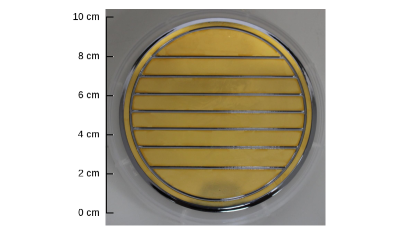
Therefore, the Si(Li) detector array plays an essential role in the GAPS detection scheme, providing the absorption depth, active area, tracking efficiency, and X-ray energy resolution necessary for this exotic atom particle identification technique. Our optimized flight detector design has an overall diameter of 10 cm, with 9 cm of active area segmented into 8 readout strips, and an overall thickness of 2.5 mm, with mm () sensitive thickness. Both 4- and 8-strip designs have been developed and proved to meet the GAPS requirement. However, the 8-strip design has been adopted for the GAPS flight instrument, as it improves tracking performance and allows use of a custom ASIC readout, while still achieving the required energy resolution [15]. This low-power ASIC reduces inactive material in the tracker and permits for lower temperature operation, and thus improved noise performance, compared to a discrete-component preamplifier readout. The detectors are arranged in 10 layers each with detectors to achieve the absorption depth necessary for incident antinuclei with energies GeV/n [14, 13]. Hence the mass production of detectors is required.
The leakage current and capacitance of each Si(Li) strip should be lower than 5 nA and 40 pF, respectively, to achieve the required energy resolution keV (FWHM) for 20100 keV characteristic X-rays [15]. To suppress the power consumption, GAPS adopts a newly-developed cooling system for the Si(Li) detectors [16, 17]. Considering all thermal and mechanical restrictions for a balloon-craft, the cooling system is designed to cool Si(Li) detectors down to C (C to C). The leakage current, which depends exponentially on temperature, must meet the requirement in this operating range. The capacitance requirement can be simultaneously achieved by realizing a thick sensitive layer. A relatively low bias voltage of 250 V is also required, because it allows for operation at the ambient flight pressure without suffering breakdown.
We have adopted Si(Li) detectors for the GAPS design, as they provide a sensitive layer thicker than a few millimeters with modest bias voltages, by compensating -type Si crystal with Li ions [18, 19]. However, a high-yield, low-cost fabrication method for large-area Si(Li) detectors, with operating temperatures of at minimum to C, currently has no experimental precedent.
Si(Li) detectors have been commercially-produced previously, mainly in the energy dispersive X-ray (EDX) spectroscopy field. However, all of these EDX Si(Li) detectors are small with a diameter of cm, and operated mainly at liquid nitrogen temperature, which is significantly lower than that required for GAPS. Several previous studies have reported on large-area Si(Li) detectors [20, 21, 22]; however, all these methods required removing the un-drifted region after the Li drift, because achieving a uniform drift across a large-area was impossible. As an approach to address this difficulty, it was demonstrated that uniform Li-drifting can be conducted into a large-area Si wafer by drifting towards a boron-implanted -side layer [23, 24, 25, 26, 27]. However, boron implantation requires annealing at C, which has the potential to damage the Si crystals and increases the fabrication cost.
Two key techniques in the GAPS Si(Li) development are a uniform Li drift in large-area Si(Li) and a suppression of leakage current at the relatively high temperature. Based on previous research on prototype detectors [28, 29, 30, 31], we have established a mass-production method for the GAPS Si(Li) detectors. Figure 1 shows an example of a GAPS Si(Li) detector.
In this paper, Sec. 2 briefly explains the overall fabrication flow of the GAPS Si(Li) detector. Detailed descriptions of the fabrication process are given in Sec. 3, where we highlight the specific developments investigated in over 50 prototype detectors. Sec. 4 demonstrates the performance and high-yield rate of the mass-produced detectors. Conclusions are presented in Sec. 5.
2 Overview of fabrication flow
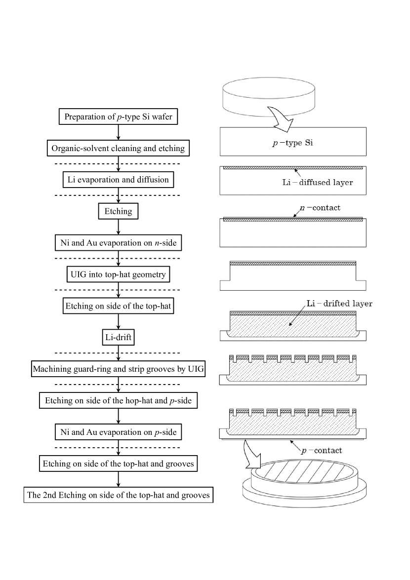
Figure 2 provides an overview of the fabrication process. First, lithium is evaporated on one surface of a -type Si wafer and diffused through a shallow depth by heating the wafer. This process supplies Li ions for compensating impurities in the -type Si, while forming a Li-diffused -layer. A metal contact is evaporated on -side after the diffusion. The wafer is machined into the top-hat geometry by ultrasonic impact grinding (UIG) to confine the Li-drifted region. Li ions in the Li-diffused layer are drifted toward the -side by applying a bias voltage to the heated wafer. During drifting, Li ions compensate impurities in the -type Si, forming a well-compensated intrinsic layer (-layer) that functions as the sensitive volume in the final detector. Grooves are machined on the -side via UIG to isolate the guard-ring structure and readout strips. A metal contact is evaporated on the -side. The GAPS Si(Li) detector is then completed by performing wet etchings and cleanings of its exposed Si surfaces.
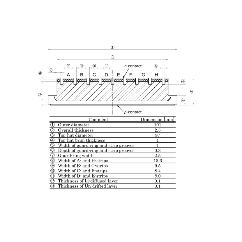
We summarize the dimensions of the mass-production model of the GAPS Si(Li) detector in Fig. 3. Displayed dimensions represent the machined dimensions by UIG. The final detectors deviate somewhat from these values mainly due to material removed during etching.
Our developments prioritize cost effectiveness for mass production while maximizing detector quality. Shimadzu Corporation, Japan, is an industry-leading company of Si(Li) EDX detectors. The fabrication apparatuses and methods herein are developed by extending the work of our previous studies [28, 29, 30, 31], while utilizing Shimadzu’s techniques for quality control and cost reduction.
3 Development
3.1 Procurement of p-type Si crystal
| Fabrication method | Floating zone |
|---|---|
| Type | p |
| Dopant | Boron |
| Crystal orientation | |
| Oxygen concentration | |
| Carbon concentration | |
| Resistivity | |
| Minority carrier lifetime | ms |
| Diameter | mm (4 inches) |
Several studies have reported that uniformly drifting Li ions into a thick, large-area, -type Si wafer is difficult mainly due to defects and contaminants, such as oxygen and carbon, in the Si crystal [20, 21, 22, 23, 32, 33, 34]. These behave as traps for Li ions and hence decrease Li ion mobility in the crystal, making it hard to uniformly drift. Previous works also demonstrate that these impurities and defects concentrate especially in the central region of Si wafer, resulting in an uncompensated region at the center of the wafer’s -side after the Li drift [22, 21, 23].
We have successfully developed a high-purity -type Si crystal specifically for the GAPS Si(Li) detectors in collaboration with SUMCO Corporation, Japan. Table 1 lists the specifications of the crystal used for our fabrications. For the raw material of our crystal growth, we employ polycrystalline silicon made from mono-silane. The crystal is grown to be oxygen free using the floating zone method with an axis of . Both Si crystals with and orientations are used in previous studies, but is more proven for Si(Li) detector fabrication, including for Shimadzu’s commercial detectors. There is also one report indicating that it is empirically preferable for Li drift [22].
Resistivity of corresponds to an acceptor concentration of [19], which is an order of magnitude lower density than that used in some of previous studies of large-area Si(Li) detectors [20, 21, 22, 23]. Substrate with a lower -type acceptor concentration requires fewer Li ions for compensation, thus reducing the temperature and time required in the diffusion process. Reduction of the heating treatment prevents the Si crystal from forming defects. The in-plane non-uniformity of the resistivity of our Si wafer is based on the measurement of sample wafers.
The lifetime of minority carriers is an indicator of crystal defects and contaminants. The lifetime of ms is enough to make a high-quality compensated region, as proven by our in-house development [31].
After procuring 2.5 mm-thick wafers cut from the 10 cm-diameter Si crystal, we remove foreign matter on the surface by organic-solvent cleaning with methanol, xylene, and acetone. We then etch the wafer surface with our etchant (a solution of hydrofluoric acid, nitric acid and acetic acid) for 2 min to remove surface contaminants and mechanical defects. Si oxide on the surface is then removed by immersing the wafer in a solution of hydrofluoric acid for 1 min.
3.2 Li evaporation and diffusion
Li is evaporated and diffused through a shallow depth, forming the -layer. The Si wafer is set in a chamber of a custom vacuum-based thermal Li evaporator by sandwiching it between a heater plate and a lower mask. The mask has a large round aperture that prevents Li from being deposited onto the other side of the wafer. Our custom heater plate realizes in-plane uniformity for heating the large-area wafer, which is a key issue for obtaining a uniform Li-diffused layer. A molybdenum evaporation boat filled with Li pieces is set under the wafer. The shutter between the wafer and the boat is closed at the beginning of the process to prevent Li oxide, on the surface of the Li pieces, from evaporating onto the wafer. The chamber is then pumped to Pa, and the heater is set to 280∘C. After confirming pressure and thermal stability, the shutter is opened and the current through the boat is increased. Li is evaporated onto the wafer surface by maintaining the current for 1 min, and the pressure and temperature are kept for another minute to diffuse Li through the shallow depth. The pressure valve is then opened. The wafer is naturally cooled to C, and extracted from the chamber. We obtain a -layer with a thickness of by this diffusion process, as confirmed by our visual inspection of the cross-section of the Si(Li) detector via copper staining (see Sec. 3.4).
The depth of the - junction formed by Li diffusion for time is expressed as [19]
| (1) |
where is the diffusion constant of Li in the Si crystal and is the Li surface concentration ( based on measurement of commercial Si(Li) [35]). The diffusion constant is obtained by [18] with -type Si crystal as
| (2) |
where is the elementary charge, is the Boltzmann constant, and is temperature in K. Our diffusion time (12 min at 280∘C and 150 min of the natural cooling time) leads to which is consistent with the practical depth , though the empirical equation (2) of the diffusion constant is derived or referred with different coefficients in each previous work [18, 22, 36, 37] and provides only an approximation.
Reference [18] indicates that the diffusion constant should decrease with lower resistivity, i.e., highly-doped silicon crystal, by the ion-pairing effect. This implies our high-purity Si crystal allows us to obtain a Li-diffused layer thick enough with a lower temperature and a shorter heating time, preventing defects from being generated in the crystal by our heating procedure. Indeed, our heating temperature and time during the diffusion are cooler and shorter than previous research on large-area Si(Li) using crystal. For example, [20] and [21] maintained the wafer at 400∘C for 15 min to form a diffused layer. Reference [22] requires the wafer to be maintained at a temperature ranging 300∘C to 400∘C for 520 min to obtain a diffused depth of 100200 .
The Li oxide layer formed on the wafer surface is removed by chemical etching for 1 min with our etchant. This etching also removes mechanical defects and contaminants from the surface.
3.3 Evaporation of n-electrode and top-hat machining
In a thermal evaporator set at room temperature and pressure of Pa, an 18 nm layer of nickel followed by a 120 nm layer of gold are evaporated onto the -side of the detector to form a metal contact. Nickel has good adhesion with the underlying Si, and gold has a high tolerance to oxidation.
The circumference of the n-side is then ground by UIG to make a top-hat geometry (see Fig. 2) and to confine the Li from drifting to the sides of the wafer during the Li drifting procedure. UIG is generally less expensive than other methods such as diamond-saw cutting, and is thus more suitable for mass production.
The geometry of the top-hat brim is designed to be as narrow as possible to maximize the detector’s active area, while still being wide enough to be used for handling the detector. The top-hat brim is preferred for handling the detector since it is -type even after the Li drift and thus does not need careful treatment (unlike the intrinsic region (-region) surface, see Sec. 3.5). As a result of this optimization, the inner diameter of the top-hat brim is set to 97 mm in the UIG machining, and the thickness is set to 1 mm, to prevent breakage during handling.
After the top-hat machining, an etch-resisting wax, Apiezon®, is dissolved in xylene and is painted on the - and -side surfaces by hand. Damaged layers and metal contaminants generated by UIG are then removed by etching on the side surface of the top-hat for 12 min. Organic-solvent cleaning with methanol, xylene, and acetone is then performed to remove the wax.
3.4 Li drift

A uniform Li-drift is achieved by our drift apparatus, which has been custom-designed for large-area Si(Li) detectors. We found that retaining a thin undrifted layer on the -side effectively suppresses the leakage current, as demonstrated in this section. The radial uniformity of the growth of the drifted region during Li drift is key to realizing this thin, uniform undrifted layer.
Li drifting is performed in a custom drift apparatus consisting of an electrically grounded heater plate, a pressure contact for applying a bias voltage, a resistance temperature detector (RTD), and a computer-based controller. The Si wafer is set on the heater plate with the -side up and, the -side connected to the grounded heater plate. The pressure contact and RTD are connected to the -electrode to apply a positive bias voltage and monitor the wafer’s temperature. The drift sequence described below is automatically managed via the computer-based controller.
Figure 4 depicts an example of the bias voltage, heater output, and leakage current during the 110 hours of the drifting routine. Our sample detector is a 10-cm Si(Li) detector. The voltage is increased step-wise, in 100 V intervals every 30 min, to prevent rapid increase of the leakage current. The insets in each panel of Fig. 4 display the variations over the first 3 hours of the drift, as the voltage is ramped up to the set-point of 600 V. In the first panel, open arrows indicate the timing of the voltage steps. In the final panel, the leakage current shows a step-like increase of mA corresponding to each voltage increase.
As Li drifts toward the -side and the depletion layer expands from the -side, the leakage current gradually increases. The Joule heat generated by the leakage current also increases. Displayed by the middle panel, heater output is automatically decreased to compensate for the Joule heat and keep the wafer at 100∘C.
At the end of the drift, the depletion layer approaches the -side. At this point, the leakage current rapidly increases, the wafer temperature exceeds 100∘C due to the Joule heat, and the heater output decreases to zero. The bias voltage is automatically turned off, i.e., the Li drift is terminated, either when the leakage current reaches 25 mA or when the heater output becomes zero. The wafer is then allowed to naturally cool to room temperature.
Under a bias voltage as high as 600 V, the depletion layer expands slightly toward the -side beyond the “- junction” formed between the drifted and undrifted layer. Thus, despite the steep increase in leakage current, a thin undrifted layer is retained on the -side of our Si(Li) detectors after the drifting process, as demonstrated in Fig. 5.
The necessary drift time () to obtain a drifted depth () under bias voltage () is given by [19]
| (3) |
The Li mobility () is related to the diffusion constant () by the Einstein relation
| (4) |
For our drift parameters, we derive h to obtain a drifted depth mm ( of the overall 2.5 mm thickness). This calculated result is comparable to our actual drift time displayed in Fig. 4. In the case that the Li drift is unexpectedly terminated before h, we resume the drift sequence.
The temperature and voltage allow us to achieve a high quality drift in an acceptable drift time ( days) for mass production. Higher bias voltage and temperature would reduce the required drift time. However, setting the wafer at a higher temperature by higher Joule heat or higher heater output will generate more hole-electron pairs, which attract Li-compensation, hence disturbing the ideal Li distribution, which should only compensate for acceptors [19]. Our drift parameters, 600 V and 100∘C, are found to be sufficiently low to fabricate uniform and thick Li-drifted.
The Li-diffused and drifted regions can be visually inspected by copper staining on a cross-section of the Li-drifted Si wafer [38, 39, 40]. In the copper-staining process, we first remove the -electrode via etching and cut the wafer into two cross-sectional pieces via diamond-saw dicing. The cross-section is then polished and immersed in a saturated solution containing a few drops of concentrated hydrofluoric acid under the illumination of white light. Electrons generated by the light are more attracted to - and -regions than -regions due to the photovoltage effect and cause the deionization of copper ions, resulting in copper deposition on the - and -regions.
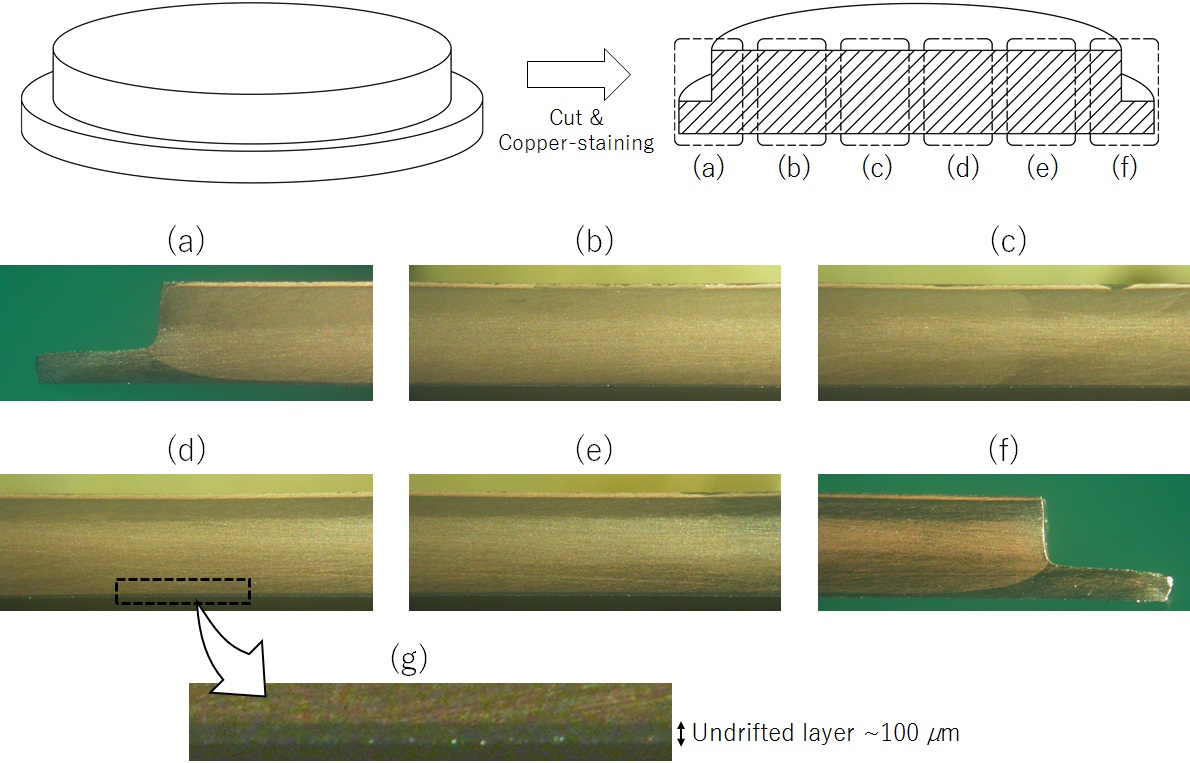
The copper-stained area is visually identified by a yellow-ish color. Figure 5 displays a cross-section of our sample detector processed by this copper-staining method. The light yellow-ish region corresponds to the Li-drifted region, whereas the darker grey-ish region filling the brim of the top-hat in Figs. 5(a) and 5(f) corresponds to the undrifted -type bulk. The thin but intense yellow-ish layer on the -side of the wafer indicates the -layer, i.e., the Li-diffused layer. We confirm via this staining that the -layer has a thickness of .
The undrifted layer is also found in Fig. 5; the dark grey-ish region seen at the brim spreads toward the center and extends to other side of the brim, keeping a thin undrifted region on the -side. Figure 5(g) displays an enlarged view of the -side region in picture (d), highlighting the undrifted layer. This undrifted layer appears uniform, with a thickness of across what will become the active region of the detector, indicating a successful uniform Li-drift.

In conventional Si(Li) detector fabrication techniques, the undrifted layer is removed to expose the Li-drifted layer on the -side. Then a metal contact such as gold is evaporated as a Schottky barrier. However, we observed excessively high leakage currents at C with a detector using this conventional contact.
Figure 6 displays the leakage current of our 10-cm diameter Si(Li) detector at C as a function of bias voltage (IV curve). In this prototype detector, the guard-ring structure described in Sec. 3.5, which is necessary to suppress the dominant surface leakage current and without which the effect of the undrifted layer is difficult to observe, had already been machined. On the contrary, machining of the strip grooves and the second etching, described in the Sections 3.5 and 3.7 respectively, were not performed in this detector. The circles in Fig. 6 display the IV curve of the detector without polishing the -side, i.e., with the undrifted layer remaining underneath the -side nickel and gold contact. This -side contact is formed after etching the -side surface, in the same manner as Sec. 3.6. After measuring this IV curve, the -side was polished to remove 40 m, leaving of undrifted layer, and the nickel and gold -side contacts were re-applied. In this manner the thickness of the undrifted layer can be reduced easily and precisely in comparison to other options such as modifying the undrifted thickness by modifying the drifting parameters.
The rectangles in Fig. 6 show the IV curve of this detector after removing 40 m of the undrifted layer. The leakage current is significantly higher than that of the unpolished detector by an order of . We next removed an additional 60 m from the -side of the detector via polishing, thus removing the entire undrifted -side layer, and re-applied the nickel and gold contacts. The resulting IV curve is indicated by the triangles in Fig. 6. The metal contact should form a Schottky barrier on the -side but the leakage current is higher than that of the unpolished detector (circles) by an order of .
This result implies that a large-area Schottky barrier contact easily breaks down at our operating temperature ( to C), which is significantly higher than that of conventional Si(Li) detectors used for X-ray spectrometry. Based on this presumption, we decided to retain the undrifted layer of on the -side to suppress the bulk leakage current, which we posit is generated in or flowing through the depletion layer via a junction between the - and -layers.
In the conventional detectors, the -contacts are used as windows for low-energy X-rays [41, 42, 43]. Therefore, such detectors adopted Schottky barrier contacts to minimize the -side insensitive layers while suppressing bulk leakage currents. Since GAPS aims to detect X-rays with energies higher than 20 keV, the insensitive layer is acceptable for the GAPS detectors.
3.5 Machining grooves for the guard-ring and strips

The exposed -region can be easily contaminated and contribute to the leakage current [19, 44]. The side surface of the top-hat has the largest area of the exposed -layer and is a major source of the leakage current. The guard-ring groove [44] is machined to suppress this surface leakage current, preventing it from flowing into the readout electronics.
After the Li-drifting process, a circular groove, with a depth and 1-mm width, is cut into the -side by UIG so that the central area, or the readout electrode of the detector, is electrically isolated from the perimeter, or guard-ring electrode (see Fig. 1). The groove is deep enough to cut through the -layer ( depth). During detector operation with a high bias voltage, the -layer between the guard ring and the active area is fully depleted and its resistivity increases dramatically to isolate the readout electrode from the guard-ring electrode.
Figure 7 displays the IV curves of a sample detector. The undrifted layer described in Sec. 3.4 had been formed in this prototype detector, but the machining of the strip grooves (described below) and the second etching (described in Sec. 3.7) were not performed. The IV curves in Fig. 7 are measured before machining the guard-ring groove (triangles); after machining the groove, with a guard-ring not connecting to any external electrode (rectangles); and after grounding the guard-ring (circles). As described in Sec. 4, negative bias voltage is applied to the -electrode, and the strips that are not being measured are connected to the ground. As shown in Fig. 7, the grounded guard-ring drastically reduces the leakage current flowing into the readout electrode by an order of in comparison to the detector without a guard-ring. This indicates that the readout electrode is successfully isolated from both the guard-ring electrode and the side surface of the detector.
Grooves that divide the active area into 8 readout strips of equal area are cut at the same time as machining the guard-ring groove, using the same groove depth and width. Under the operating bias voltage, the strips are electrically isolated from each other by the same principle as the guard-ring.
A narrower groove width is preferable because the exposed -layer in the groove can generate leakage current. However, it is important to note that UIG is limited by the width of its grinding tool. An extremely thin tool is difficult to make and is easily damaged in the UIG process. A narrower groove also has disadvantages for groove etchings. If the groove is too narrow, bubbles generated via chemical reactions in the etching process stick to the groove surface. The bubbles make it difficult to etch uniformly and sufficiently. We optimized the UIG tool for the mass-production model of the GAPS Si(Li) detector and deduced the optimal groove width as 1 mm.
The guard-ring width, i.e., width of the perimeter electrode in Fig. 1, is also optimized. A narrow guard-ring electrode is preferable to make the active area as wide as possible. However, it is difficult to precisely paint etch-resisting wax, which is necessary during the groove etching process, onto a narrow guard ring. We deduced that the optimal guard-ring width is 2.5 mm.
3.6 Forming -side contact
Wax is painted on the -side including the grooves. Then, the side surface of the top-hat and the -side surface are etched for 1 min. After the wax is removed by an organic solvent, the metal contact on the -side is evaporated in the same manner as Sec. 3.3.
3.7 Etching on side of the top-hat and grooves
The side of the top-hat and the -side grooves are etched after painting wax on the - and -electrodes. This last etching not only removes the damaged layer in the grooves formed by UIG in Sec. 3.5 but also smooths the surfaces and removes contaminants from all areas of exposed silicon. Organic-solvent cleaning is performed after this etching to remove the wax. It is assumed that this cleaning with methanol produces a lightly -type surface on the exposed -region, which ensures no electric breakdown of the detector under the high bias voltage [19, 45].
An optimized etching time is required because etching for too long not only decreases the active area but also expands the area in which the -layer is exposed. This area is easily contaminated, which increases leakage current. The number of separate etchings is also a key parameter. The wax is painted by hand, creating a non-uniform line at the edge of the painted area and thus introducing non-uniformities to the edge of the electrode after etching. Bubbles generated in the etchant also make the surface state non-uniform. Repeating the wax painting and the etching reduces these irregularities.
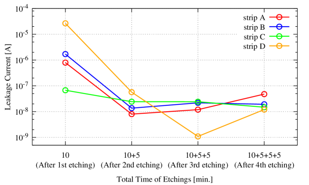
We surveyed the optimal etching time and number of discrete wax painting and etching processes. Figure 8 displays the leakage current of each strip of a prototype detector with 4 strips (AD) at a bias voltage of 200 V and a temperature of C. The leakage current is displayed as a function of the cumulative etching time or the total number of etchings. The first etching is performed for 10 min, whereas the second, third, and fourth etchings are 5 min each. Leakage currents in all strips are clearly reduced after the second etching, i.e., cumulative etching time of 15 min, compared to that after the first etching. It was also confirmed by a visual inspection that the groove surfaces are clearly smoothed and glassy after the second etching compared to after the first etching. The leakage currents are not significantly affected after the additional third and fourth etchings. This result indicates that the 15 min of etching in two discrete etching procedures is sufficient to minimize the surface leakage current.
4 Performance of the mass-produced detectors
Ten prototype detectors (test detectors) were fabricated to validate and fix the mass-production process. Then, the mass production of the flight detectors had been started. In this section, we evaluate leakage currents and capacitances of these mass-produced detectors (10 test detectors and 10 flight detectors), which were fabricated by identical procedures. Thanks to the sufficiently low leakage currents, it has been confirmed that energy resolution keV (FWHM) for 20100 keV X-rays are achieved [46]. Details of the energy resolution measurements are described in a separate publication [15].
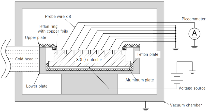
Figure 9 illustrates the setup for the IV curve measurement. The detector is mounted in a vacuum chamber set at Pa. A Teflon plate mounted on the lower plate of the detector holder electrically isolates the -electrode of the detector from the lower plate, which is fixed to the chamber and connected to the ground. An aluminum plate between the Teflon plate and the detector applies negative bias voltage to the -electrode. The upper plate of the holder is bolted to the lower plate, holding in place a Teflon ring pressed against the guard-ring. The detector is fixed by this pressure. Copper foils are pasted on the Teflon ring to electrically connect the guard-ring and the upper plate; therefore, the guard-ring electrode is grounded via the chamber.
A cold head bolted to the detector holder is cooled by a Stirling cooler. The detector is cooled by the thermal connections to the holder through the copper foils, Teflon ring, alminum plate, and Teflon plate. Calibration of the cooler was performed using a dummy wafer on which an RTD was used to monitor the detector’s temperature.
All strips of the detector are connected to the hermetic connector mounted on the side of the chamber via probes made of gold wires. The gold wire probe is selected to prevent damage to the strip electrodes on the detector. Using a multimeter, we verify the electrical connections between the hermetic connector and strips and reasonable resistivities between the strips, guard-ring, and -electrode, each time the detector is set. The strip to be measured is connected to a picoammeter or capacitance meter while the other strips are connected to the ground outside the chamber.
For the picoammeter, capacitance meter, and bias supply, HP 4140B, HP 4280A, and ORTEC 428 were used, respectively. Recently the picoammeter and bias supply were replaced with a Keithley 6487 picoammeter, which has an internal bias supply. We constructed an automatic IV measurement system controlled by LabVIEW software with this Keithley picoammeter. It will improve the speed of the mass production of the GAPS flight detectors in terms of detector evaluation.
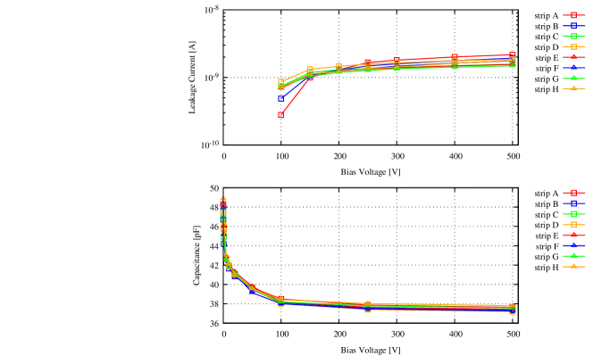
The upper panel of Fig. 10 displays IV curves of 8 strips of a sample detector at C. The leakage current of each strip is stable and is nA at our operating voltage (200300 V), significantly lower than the requirement, nA [15]. The capacitance as a function of the bias voltage in the lower panel of Fig. 10 reaches the minimum by V, indicating the detector is fully depleted around this voltage. The capacitance of pF also meets the requirement and corresponds to the thickness of the depletion layer [19],
| (5) |
for a strip area of . This is of the 2.5 mm total detector thickness. The uniformity of the capacitance, with a fluctuation of between strips, indicates a uniform Li-drifted layer.
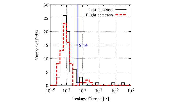
Figure 11 displays histograms of the leakage current measured for all strips of the 10 test detectors and 10 flight detectors. The bias voltage and the temperature are set at 250 V and C, respectively. In 80 strips of the 10 test (10 flight) detectors, 73 (75) strips have the leakage currents below 5 nA. Our acceptance criteria of the leakage current of each detector, that at least 7 strips out of 8 must have leakage currents 5 nA, was satisfied by 9/10 test detectors and 9/10 flight detectors. All strips of the test and flight detectors pass our acceptance criteria of the capacitance, 42 pF at 250 V at room temperature, and we confirmed that the capacitances at C stays within 97-99% of the room temperature value for all 80 strips of the test detectors. Capacitances of the flight detectors at cold temperature are not measured in our mass-production scheme to cut the lead-time of the mass production.
5 Conclusions
We have developed and established, for the first time, a high-yield fabrication method for large-area Si(Li) detectors operated at relatively high temperature. Our 10 cm-diameter -type crystal is verified to have sufficiently low impurity concentrations and radial non-uniformities to fabricate a uniform Li-drifted layer. While a large-area Schottky barrier contact on the -side can easily break down at C, our optimized drift sequence retains a uniform undrifted layer on the -side with a thickness of , which drastically reduces bulk leakage current. The guard-ring groove and optimized etching process are also confirmed to effectively reduce the leakage current.
Our Si(Li) detector design has a sensitive layer with a mm depth, depth of the overall detector thickness of 2.5 mm, and an overall diameter of 10 cm, with 9 cm of active area. The detector is segmented into 8 readout strips and the operating temperature is C. Based on the 20 mass-produced detectors we have produced, the production yield is sufficiently high (90%) at this point. The detectors’ leakage currents and capacitances are low enough to achieve keV energy resolution for 20100 keV X-rays. Good uniformity of the capacitance between strips indicates that the detector volume is uniformly compensated by our Li drift. This is also confirmed by copper staining on cross-sections of sample Si(Li) detectors.
The mass production of GAPS Si(Li) detectors was started in late 2018 and will extend through early 2020.
Acknowledgements
We thank SUMCO Corporation and Shimadzu Corporation for their co-operation in our detector development.
M. Kozai is supported by the JSPS KAKENHI under Grant No. JP17K14313. H. Fuke is supported by the JSPS KAKENHI under Grants No. JP2670715 and JP17H01136. K. Perez receives supports from the Heising-Simons Foundation, the Alfred P. Sloan Foundation, and the ULVAC-Hayashi MISTI Seed Fund. F. Rogers is supported through the National Science Foundation Graduate Research Fellowship under Grant No. 1122374.
This work was partially supported by the JAXA/ISAS Small Science Program in Japan and the NASA APRA program through Grant NNX17AB44G in the US.
We are grateful to all GAPS collaborators.
References
References
- [1] T. Aramaki, S. Boggs, S. Bufalino, L. Dal, P. von Doetinchem, F. Donato, N. Fornengo, H. Fuke, M. Grefe, C. Hailey, B. Hamilton, A. Ibarra, J. Mitchell, I. Mognet, R. A. Ong, R. Pereira, K. Perez, A. Putze, A. Raklev, P. Salati, M. Sasaki, G. Tarle, A. Urbano, A. Vittino, S. Wild, W. Xue, K. Yoshimura, Review of the theoretical and experimental status of dark matter identification with cosmic-ray antideuterons, Physics Reports 618 (2016) 1–37.
- [2] C. J. Hailey, An indirect search for dark matter using antideuterons: the GAPS experiment, New J. Phys. 11 (105022) (2009) 1–15.
- [3] C. J. Hailey, T. Aramaki, S. E. Boggs, P. v. Doetinchem, H. Fuke, F. Gahbauer, J. E. Koglin, N. Madden, S. A. I. Mognet, R. Ong, T. Yoshida, T. Zhang, J. A. Zweerink, Antideuteron based dark matter search with GAPS: Current progress and future prospects, Adv. Space Res. 51 (2013) 290–296.
- [4] H. Fuke, T. Aramaki, S. Boggs, W. W. Craig, P. v. Doetinchem, L. Fabris, C. J. Hailey, F. Gahbauer, T. Gordon, C. Kato, A. Kawachi, T. Koike, M. Kozai, N. Madden, S. A. I. Mognet, K. Mori, K. Munakata, S. Okazaki, R. A. Ong, K. Perez, K. Sakimoto, Y. Shimizu, N. Yamada, A. Yoshida, T. Yoshida, K. P. Ziock, J. Zweerink, Present status and future plans of GAPS antiproton and antideuteron measurement for indirect dark matter search, JPS Conf. Proc. 18 (011003) (2017) 1–6.
- [5] F. Donato, N. Fornengo, P. Salati, Antideuterons as a signature of supersymmetric dark matter, Phys. Rev. D 62 (043003) (2000) 1–13.
- [6] F. Donato, N. Fornengo, D. Maurin, P. Salati, R. Taillet, Antiprotons in cosmic rays from neutralino annihilation, Phys. Rev. D 69 (063501) (2004) 1–19.
- [7] R. Duperray, B. Baret, D. Maurin, G. Boudoul, A. Barrau, L. Derome, K. Protasov, M. Buénerd, Flux of light antimatter nuclei near earth, induced by cosmic rays in the galaxy and in the atmosphere, Phys. Rev. D 71 (083013) (2005) 1–22.
- [8] A. Cuoco, M. Kramer, M. Korsmeier, Novel dark matter constraints from antiprotons in light of AMS-02, Phys. Rev. Lett. 118 (191102) (2017) 1–6.
- [9] M. Korsmeier, F. Donato, N. Fornengo, Prospects to verify a possible dark matter hint in cosmic antiprotons with antideuterons and antihelium, Phys. Rev. D 97 (103011) (2018) 1–11.
- [10] I. V. Moskalenko, A. W. Strong, J. F. Ormes, M. S. Potgieter, Secondary antiprotons and propagation of cosmic rays in the galaxy and heliosphere, Astrophys. J. 565 (2002) 280–296.
- [11] S. Lin, X. Bi, J. Feng, P. Yin, Z. Yu, Systematic study on the cosmic ray antiproton flux, Phys. Rev. D 96 (123010) (2017) 1–13.
- [12] V. Bindi, C. Corti, C. Consolandi, J. Hoffman, K. Whitman, Overview of galactic cosmic ray solar modulation in the AMS-02 era, Adv. Space Res. 60 (2017) 865–878.
- [13] T. Aramaki, S. E. Boggs, P. von Doetinchem, H. Fuke, C. J. Hailey, S. A. I. Mognet, R. A. Ong, K. Perez, J. Zweerink, Potential for precision measurement of low-energy antiprotons with GAPS for dark matter and primorial black hole physics, Astropart. Phys. 59 (2014) 12–17.
- [14] T. Aramaki, C. J. Hailey, S. E. Boggs, P. von Doetinchem, H. Fuke, S. I. Mognet, R. A. Ong, K. Perez, J. Zweerink, Antideuteron sensitivity for the GAPS experiment, Astropart. Phys. 74 (2016) 6–13.
- [15] F. Rogers, M. Xiao, K. Perez, T. Erjavec, L. Fabris, H. Fuke, C. Hailey, M. Kozai, A. Lowell, N. Madden, M. Manghisoni, S. McBride, V. Re, E. Riceputi, N. Saffold, Y. Shimizu, Large-area Si(Li) detectors for X-ray spectrometry and particle tracking in the GAPS experiment, submitted, arXiv e-prints (2019) 1–17.
- [16] H. Fuke, T. Abe, T. Daimaru, T. Inoue, A. Kawachi, H. Kawai, Y. Masuyama, H. Matsumiya, D. Matsumoto, Y. Miyazaki, J. Mori, H. Nagai, T. Nonomura, H. Ogawa, S. Okazaki, T. Okubo, S. Ozaki, D. Sato, K. Shimizu, K. Takahashi, S. Takahashi, N. Yamada, T. Yoshida, Development of a cooling system for GAPS using oscillating heat pipe, Trans. JSASS Aerospace Tech. Japan 14 (2016) 17–26.
- [17] S. Okazaki, H. Fuke, H. Ogawa, Y. Miyazaki, K. Takahashi, N. Yamada, Meter-scale multi-loop capillary heat pipe, Applied Thermal Engineering 141 (2018) 20–28.
- [18] E. M. Pell, Ion drift in an - junction, J. Appl. Phys. 31 (1960) 291–302.
- [19] F. S. Goulding, Semiconductor detectors for nuclear spectrometry, I, Nucl. Instr. Methods 43 (1966) 1–54.
- [20] T. Miyachi, S. Ohkawa, T. Emura, M. Nishimura, O. Nitoh, K. Takahashi, S. Kitamura, Y. Kim, T. Abe, A thick and large active area Si(Li) detector, Jpn. J. Appl. Phys. 27 (1988) 307–310.
- [21] T. Miyachi, S. Ohkawa, H. Matsuzawa, T. Otogawa, N. Kobayashi, Y. Ikeda, H. Onabe, Development of lithium-drifted silicon detectors using and automatic lithium-ion drift apparatus, Jpn. J. Appl. Phys. 33 (1994) 4115–4120.
- [22] T. Kashiwagi, J. Kikuchi, T. Nakasugi, A. Nakamoto, A fabrication method and problems of large area Si(Li) detector, Report of Waseda Research Institute for Science and Engineering 128 (1990) 66–80.
- [23] H. Onabe, H. Kume, M. Obinata, T. Kashiwagi, Development of Si(Li) detectors for charged particles spectrometer, Ionizing Radiation 28 (2002) 159–167.
- [24] C. S. Tindall, M. Amman, P. N. Luke, Large-area Si(Li) orthogonal-strip detectors, IEEE Trans. Nucl. Sci. 51 (3) (2004) 1140–1143.
- [25] D. Protić, T. Krings, R. Schleichert, Development of double-sided microstructured Si(Li) detectors, IEEE Trans. Nucl. Sci. 49 (2002) 1993–1998.
- [26] D. Protić, T. Krings, Development of transmission Si(Li) detectors, IEEE Trans. Nucl. Sci. 50 (2003) 1008–1012.
- [27] D. Protić, E. Hull, T. Krings, K. Vetter, Large-volume Si(Li) orthogonal-strip detectors for compton-effect-based instruments, IEEE Trans. Nucl. Sci. 52 (2005) 3181–3185.
- [28] T. Aramaki, S. E. Boggs, W. W. Craig, H. Fuke, F. Gahbauer, C. J. Hailey, J. E. Koglin, N. Madden, K. Mori, R. A. Ong, T. Yoshida, Antideuterons as an indirect dark matter signature: Si(Li) detector development and a gaps balloon mission, Adv. Space Res. 46 (2010) 1349–1353.
- [29] T. Aramaki, S. K. Chan, C. J. Hailey, P. A. Kaplan, T. Krings, N. Madden, D. Protić, C. Ross, Development of large format Si(Li) detectors for the GAPS dark matter experiment, Nucl. Instr. Methods A 682 (2012) 90–96.
- [30] K. Perez, T. Aramaki, A. Brickman, C. Hailey, G. Kewley, N. Madden, S. Mechbal, G. Tajiri, Progress on large-scale, low-cost Si(Li) detector fabrication for the GAPS balloon mission, In 2013 IEEE Nuclear Science Symposium and Medical Imaging Conference (2013 NSS/MIC) 1–3.
- [31] K. Perez, T. Aramaki, C. J. Hailey, R. Carr, T. Erjavec, H. Fuke, A. Garvin, C. Harper, G. Kewley, N. Madden, S. Mechbal, F. Rogers, N. Saffold, G. Tajiri, K. Tokuda, J. Williams, M. Yamada, Fabrication of low-cost, large-area prototype Si(Li) detectors for the GAPS experiment, Nucl. Instr. Methods A 905 (2018) 12–21.
- [32] H. M. Murray, J. W. Harpster, K. J. Casper, Fabrication methods for lithium drifted surface barrier silicon detectors, Nucl. Instr. Methods 40 (1966) 330–336.
- [33] A. Fong, J. T. Walton, E. E. Haller, H. A. Sommer, J. Guldberg, Characterization of large diameter silicon by low-bias charge collection analysis in Si(Li) PIN diodes, Nucl. Instr. Methods 199 (1982) 623–630.
- [34] P. G. Litovchenko, W. Wahl, D. Bisello, R. Rando, A. P. Litovchenko, V. F. Lastovetsky, L. I. Barabash, T. I. Kibkalo, L. A. Polivtsev, J. I. Kolevatov, V. P. Semenov, L. A. Trykov, J. Wyss, Silicon detectors for -ray and -spectroscopy, Nucl. Instr. Methods A 512 (2003) 408–411.
- [35] M. Yamada, Shimadzu’s internal report, Unpublished (2016) 1–12.
- [36] C. S. Fuller, J. C. Severiens, Mobility of impurity ions in germanium and silicon, Phys. Rev. 96 (1954) 21–25.
- [37] J. P. Maita, Ion pairing in silicon, J. Phys. Chem. Solids 4 (1958) 68–70.
- [38] P. J. Whoriskey, Two chemical stains for making - junctions in silicon, J. Appl. Phys. 29 (1958) 867–868.
- [39] P. A. Iles, P. Coppen, Location of - and - junctions in semiconductors, Br. J. Appl. Phys. 11 (1960) 177–184.
- [40] H. Kume, H. Onabe, M. Obinata, T. Kashiwagi, Evaluation of Si(Li) detectors by a combination of the copper plating method and X-ray analytical microscopy, IEEE Trans. Nucl. Sci. 48 (2001) 1012–1015.
- [41] C. E. Lyman, D. B. Williams, J. I. Goldstein, X-ray detectors and spectrometers, Ultramicroscopy 28 (1989) 137–149.
- [42] C. S. Rossington, J. T. Walton, J. M. Jaklevic, Si(Li) detectors with thin dead layers for low energy X-ray detection, IEEE Trans. Nucl. Sci. 38 (1991) 239–243.
- [43] C. E. Cox, D. A. Fischer, W. G. Schwarz, Y. Song, Improvement in the low energy collection efficiency of Si(Li) X-ray detectors, Nucl. Instr. Methods B 241 (2005) 436–440.
- [44] F. S. Goulding, W. L. Hansen, Leakage current in semiconductor junction radiation detectors and its influence on energy-resolution characteristics, Nucl. Instr. Methods 12 (1961) 249–262.
- [45] J. Llacer, Study of surface effects in thick lithium drifted silicon radiation detectors, IEEE Trans. Nucl. Sci. 11 (1964) 221–231.
- [46] M. Kozai, H. Fuke, M. Yamada, T. Erjavec, C. Hailey, C. Kato, N. Madden, K. Munakata, K. Perez, F. Rogers, N. Saffold, Y. Shimizu, K. Tokuda, M. Xiao, Development of large-area lithium-drifted silicon detectors for the GAPS experiment, In 2018 IEEE Nuclear Science Symposium and Medical Imaging Conference (2018 NSS/MIC), arXiv e-prints (2018) 1–4.