Imaging graphene field-effect transistors on diamond using nitrogen-vacancy microscopy
Abstract
The application of imaging techniques based on ensembles of nitrogen-vacancy (NV) sensors in diamond to characterise electrical devices has been proposed, but the compatibility of NV sensing with operational gated devices remains largely unexplored. Here we fabricate graphene field-effect transistors (GFETs) directly on the diamond surface and characterise them via NV microscopy. The current density within the gated graphene is reconstructed from NV magnetometry under both mostly p- and n-type doping, but the exact doping level is found to be affected by the measurements. Additionally, we observe a surprisingly large modulation of the electric field at the diamond surface under an applied gate potential, seen in NV photoluminescence and NV electrometry measurements, suggesting a complex electrostatic response of the oxide-graphene-diamond structure. Possible solutions to mitigate these effects are discussed.
I Introduction
Sensing techniques using nitrogen-vacancy (NV) centres in diamond Doherty et al. (2013) provide a convenient platform by which condensed matter systems can be interrogated Casola et al. (2018). The local sensitivity of NV centres to both magnetic and electric fields, in concert with their flexible experimental conditions Rondin et al. (2014), permit both sensing and imaging of a range of nano- to meso-scale phenomena. An application of these techniques is the characterisation of electrical devices and related materials. Magnetic noise spectroscopy has been used to probe and map the local conductivity of thin metallic films Kolkowitz et al. (2015); Ariyaratne et al. (2018), lending insight to the motion of carriers within the material, and also to identify noise sources from sparse metallic depositions Lillie et al. (2018). In low dimensional systems, magnetic noise spectroscopy should provide insight into local electronic correlations Agarwal et al. (2017); Rodriguez-Nieva et al. (2018), whereas static magnetic field mapping has been used to map charge transport in carbon nano-tubes using scanning single-NV centres Chang et al. (2017), and monolayer graphene ribbons via wide-field imaging experiments Tetienne et al. (2017). Extensions to the latter scenario should be able to measure signatures of viscous electron flow in graphene and similar systems Bandurin et al. (2016); Guerrero-Becerra et al. (2019); Ku et al. (2019), and other mesoscopic effects such as electron-hole puddling Martin et al. (2008), and gate controlled steering of carriers Williams et al. (2011).
Wide-field imaging of electrical devices using NV ensembles generally requires the devices to be fabricated directly on the NV-diamond substrate, while many interesting transport phenomena require precise control over the doping in the conductive channel. This can be achieved in a field-effect transistor (FET) device, employing either a top gate Kim et al. (2008); Andersen et al. (2019); Ku et al. (2019), an in-plane gate Hähnlein et al. (2012); Hauf et al. (2014), or an electrolytic gate Ohno et al. (2009). Recently, graphene based devices have been fabricated successfully on NV diamond substrates Tetienne et al. (2017); Andersen et al. (2019); Ku et al. (2019), but the compatibility of such structures with wide-field NV microscopy remains largely unexplored, with questions of whether the operating conditions required for NV microscopy may affect the operation and integrity of the FET, or whether the fabrication/operation of the FET may affect the ability to perform NV sensing.
In this work, we fabricate a number of top-gated graphene field-effect transistors (GFETs) on an NV-diamond substrate, and characterise device phenomena via wide-field imaging of the near-surface NV ensemble. Current is injected into the graphene ribbons, , by application of a source-drain potential, , and the doping of the ribbon is tunable via a top gate potential, , allowing charge transport to be probed in different doping regimes, and for the effect of the gate to be studied [Fig. 1(a)]. Firstly, the devices are characterised by electrical measurements and the influence of the laser, used to excite the NV-layer, is assessed. Secondly, the current density within the graphene ribbon is reconstructed under p- and n-type doping by measuring the associated Ørsted field via optical readout of the NV electron-spin resonances. Thirdly, an effect is observed by which the NV-layer photoluminescence (PL) is modulated by the applied gate potential in regions proximal to the gated device, but extending up to m away from the graphene ribbon. Direct measurement of the electric field by the NV ensemble electron-spin resonances demonstrate that this effect is due to an enhanced electric field surrounding the graphene ribbon which diminishes the NV-/NV0 charge state ratio. Finally, we discuss possible solutions to overcome the challenges identified in this study, to facilitate further investigation of transport phenomena in graphene and other two-dimensional materials.
II Fabrication
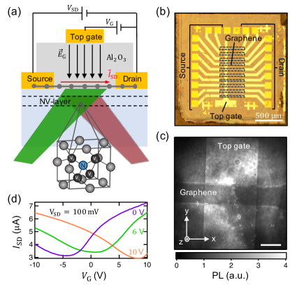
Graphene field-effect transistors (GFETs) were fabricated on NV-diamond substrates by using a standard wet chemical method Liang et al. (2011) to transfer monolayer graphene to the substrate from commercially available CVD polycrystalline graphene on Cu foil. The transferred graphene was selectively etched into m or m wide ribbons in an oxygen plasma with a photolithographic resist mask. Multiple photolithography steps were used to create the Cr/Au / nm source and drain contacts, wire bonding pads and the top gate contact [Fig. 1(b)]. Atomic layer deposition (ALD) with modified precursor pulses was used to grow an nm Al2O3 dielectric layer directly on the graphene ribbons without the use of a nucleation layer Aria et al. (2016) (appendix B). The diamond substrates used in these experiments feature an NV-layer formed by ion implantation nm below the surface (appendix A).
III Gating effect and laser
After fabrication, the devices were imaged via the NV-layer PL, using a nm continuous wave (CW) laser to excite the NV ensemble, and collecting the PL on an sCMOS camera, filtered around the NV- phonon side band at nm [Fig. 1(c)]. Direct visualisation of the graphene is made possible by a Förster resonant energy transfer (FRET) interaction between the graphene ribbon and the near-surface NV-layer, which quenches the PL Tisler et al. (2013). The top gate appears brighter due to enhanced illumination at the NV-layer under the gate, due to a standing wave formed with the reflected light Tetienne et al. (2019).
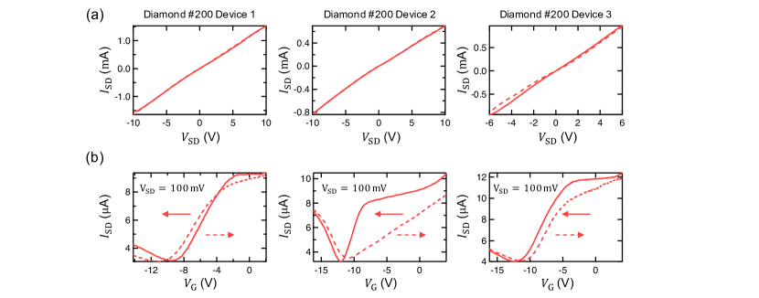
Electrical characterisation of the devices found source-drain resistances varying between k and k for the m wide devices ( m between source to drain contacts), and between k and k for the m wide devices ( m between source to drain contacts), and good Ohmic behaviour (appendix C). Applying a small source drain potential, mV, and measuring the source-drain current, , while sweeping the gate potential, , a conductivity minimum was found for most devices (appendix C). The conductivity minima, which indicate the charge neutrality point, were found to shift significantly depending on the measurement conditions and the history of the device, specifically, the applied gate potential and illumination conditions prior to the measurement [Fig. 1(d)]. We attribute this to a photon assisted charge transfer between the graphene and the oxide (appendix C), similar to the optical-doping seen with other gate dielectrics and substrates Kim et al. (2013); Landois et al. (2013); Ju et al. (2014). In addition to the photo-doping effect, we observe hysteresis in our versus measurements, even when measuring in the dark (appendix C). The hysteresis is likely due to screening of the electric field associated with the gate potential by an accumulation of trapped charge at both the graphene-oxide interface and within the oxide bulk. This has been demonstrated to cause similar hysteresis in graphene devices on SiO2 Lee et al. (2011); cheng Mao et al. (2016), and may also be associated with the defect density within the graphene itself Krishna Bharadwaj et al. (2016). The presence of the laser is likely to exacerbate this situation by creating additional trapped mobile charges within the oxide Ha (2014). The photo-doping induced by the laser is reproducible and sufficiently stable under fixed illumination and gate potentials to maintain the selected majority carrier type (appendix C) over time frames compatible with current density mapping.
IV Transport mapping under doping
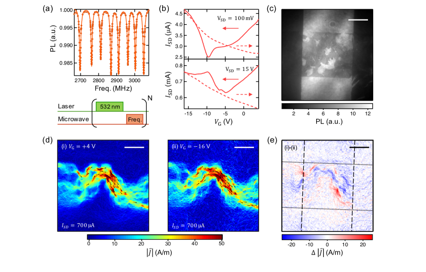
Previously, NV ensemble measurements have been used to reconstruct current densities within graphene ribbons from the associated Ørsted field as measured by optically detected magnetic resonance (ODMR) Tetienne et al. (2017). Here we apply the same methodology, with the aim of producing current density maps in both the p-type and the n-type doped regimes. The ODMR measurement was performed with a background magnetic field oriented such that the two electron-spin resonance (ESR) transitions of each of the four NV orientations are individually resolvable [Fig. 2(a)]. Each transition frequency is identified by a reduction in PL as the NV spin-state is driven from the pumped bright state, , to the less fluorescent states, . The magnetic field vector at each pixel is determined by fitting the ESR frequencies, which are shifted by the graphene Ørsted field via the Zeeman effect, and determining the corresponding field projection along each of the four NV-family axes. Subtracting the background field due to the biasing permanent magnet, the measured Ørsted field is extracted, from which the current density within the graphene ribbon is reconstructed by inverting the Biot-Savart law in Fourier space (appendix D). We note that in these devices, unlike in Ref. Tetienne et al. (2019), no apparent current leakage into the diamond was observed (appendix D).
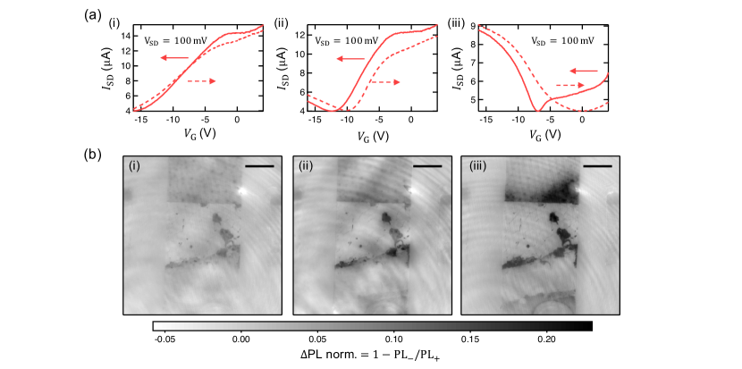
Prior to mapping current densities, the device was characterised electrically to identify n- and p-type doping regimes under the conditions used for current density mapping, which require a comparatively high source-drain potential. was measured over a range of V to V, with mV [Fig. 2(b) upper] and V [Fig. 2(b) lower], both under CW laser illumination. Prior to each sweep, the device resistance was left to equilibrate at the initial gate potential under laser illumination, such that the sweep is representative of the device after photo-doping and inter-facial charge accumulation. For the decreasing gate potential sweeps (solid curves), conductivity minima are observed at V for the smaller , and V for the larger , which also shows a different shape in the transport curve. This is likely due to being referenced to the drain contact, and being of comparable magnitude to in this scenario. For the increasing sweeps (dashed curves), we observe conductivity minima at V and V for the lower and higher scenarios respectively, where the end of range is set to mitigate leakage current through the oxide. Accounting for the gate potential dependent photo-doping, we conclude that fixed gate potentials of V and V give n- and p-type doping of the graphene ribbon respectively, which should be maintained under subsequent laser pulsing (appendix C), and hence move to acquire current density maps under each of these conditions.
A PL image of the mapped device shows the m wide graphene ribbon with a number of tears across the gated region, which arise during transfer and fabrication [Fig. 2(c)]. Throughout imaging we maintain a constant total injected current of A, giving a that varies around V. The reconstructed current density maps of the GFET under n-type [Fig. 2(d)(i)] and p-type [Fig. 2(d)(ii)] doping show broadly similar features, where the current density is increased under the gated area as carriers are restricted to narrow passages due to the tears in the graphene. Taking a subtraction of the norm current density at each pixel between the two doping conditions shows clear differences in the current path [Fig. 2(e)]. Some of these variations are associated with degradation of the graphene channel throughout the measurement at V, however, some are uncorrelated with changes to the graphene visible at our imaging resolution (appendix D). Degradation of the devices throughout measurement precludes further investigation into the origin of these differences, however, in principle such effects could arise from inhomogeneous doping of the graphene channel, gate controlled steering of carriers Williams et al. (2011), gate induced changes to the density of charged impurities and defects that have an asymmetric scattering cross section for electrons and holes Adam et al. (2007); Hwang et al. (2007); Wehling et al. (2010); Campos et al. (2013); Bai et al. (2015).
V PL switching effect
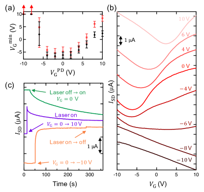
While varying the gate potential in the previous measurement, we observed that the total PL of the NV ensemble varied significantly with the applied gate potential. To investigate this effect, a measurement was performed in which the PL was accumulated under CW laser illumination as the gate potential was varied. A settling time was introduced between setting the gate potential and starting the PL accumulation, which itself was integrated over a number of camera cycles to average out fluctuations in the illuminating laser intensity. A small source-drain potential, mV, was applied to track the device conductivity throughout the measurement.
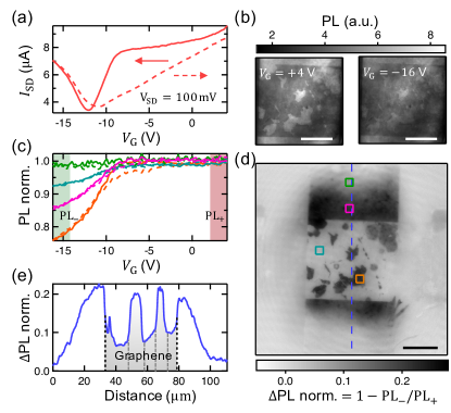
This measurement was made on the same device in which current densities were mapped. The gate potential is swept across from V to V and back, encompassing the neutrality point of the device, which is seen at approximately V [Fig. 3(a)]. The device resistance is left to equilibrate at V under laser illumination prior to sweeping. Comparing snapshots of the accumulated PL images at the extrema of the gate potential sweep [Fig. 3(b)] demonstrates a clear quenching of the PL near the graphene ribbon under the gate at the lower gate potential. Looking at area normalised PL curves around the device, we see that the PL is constant above V, then declines by up to % in regions close to, but not directly beneath the graphene [Fig.3(c)]. To map the extent of this effect, we take a normalised difference between the PL averaged across a V window at either end of the sweep, PL- and PL+ in Fig. 3(c), and plot this difference across the full field of view [Fig. 3(d)]. The normalised PL difference images shows the PL switching effect occurs only under the top gate, in regions un-screened by the graphene. Surprisingly this effect extends laterally from the graphene ribbon by up to m [Fig. 3(e)]. We note that the magnitude of this PL change increases throughout the lifetime of the device (appendix C).
A likely explanation for this gate potential dependent PL, is that varying the gate potential affects the charge distribution at the diamond-oxide interface, and hence the degree of band bending across the NV-layer Broadway et al. (2018). This effect has been investigated previously by varying the surface chemistry of the diamond Hauf et al. (2011); Cui and Hu (2013) and by electrostatic gating of NV centres Grotz et al. (2012); Hauf et al. (2014); Pfender et al. (2017). Here, we suggest that an increasing gate potential populates an acceptor layer at the diamond surface Stacey et al. (2019), given the low carrier density within the implanted region, and hence increases the band bending across the NV-layer. As the band bending increases, the Fermi level falls below the NV- charge state at greater depths within the diamond. Once this occurs around the mean depth of the NV ensemble, the PL of the layer is reduced significantly as NV0 becomes the dominant charge state. The comparative abundance of charge carriers in the graphene is expected to screen this effect, and hence we only observe the PL switching close to the gated device, but not directly under the graphene ribbon. We note that the charge state stability and dynamics under illumination and in the dark may also be altered by the gate potential through the local charge environment within the diamond Dhomkar et al. (2018); Bluvstein et al. (2019).
VI Electric field measurements
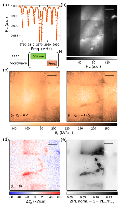
In order to test the outlined hypothesis, a direct measurement of the electric field was made. The electric field across the NV-layer can be measured in a direct and quantitative manner via the Stark effect on the NV spin-states Doherty et al. (2013). To do this, we performed an ODMR measurement, as for the previous Ørsted field measurements, but with the biasing magnetic field oriented such that the magnetic field projection along a single NV-family is minimised, enhancing its electric-field sensitivity Dolde et al. (2011); Broadway et al. (2018), but still allowing each spin-state transition of that family to be resolved [Fig. 4(a)]. The optical contrast of these transitions was selectively enhanced by rotating the linear polarisation of the excitation laser to further improve sensitivity Alegre et al. (2007).
The electric field was mapped across a single GFET device [Fig. 4(b)] for applied gate potentials of V, and V [Fig. 4(c)]. In both measurements, the electric field is approximately kV/cm less in the NV-layer under the graphene ribbon than that directly under the oxide. This may be partially due to the graphene modifying surface space-charge distribution at the diamond surface, and hence decreasing the band bending, however, it is more likely to be fully explained by FRET effect with the graphene quenching PL from NV centres closer to the surface, biasing the PL collection to deeper NVs which see a lower electric field. At V, the electric field increases at the edges and within tears in the graphene ribbon under the top gate. These features are highlighted in taking a subtraction of the two maps [Fig. 4(d)], which shows an enhanced electric field up to kV/cm in these regions, and essentially no change under the graphene ribbon.
Comparing the electric field map to the difference in normalised PL of the same device [Fig. 4(e)], we see a strong correlation in the location of features showing an enhanced electric field and reduced PL at high gate potential. The correspondence between the directly measured electric field and the gate potential dependent PL validates the claim that PL dependence on gate potential arises from electric field mediated band bending within the diamond Broadway et al. (2018). The spatial distribution of this effect, namely that it extends up to m from the gated device, is less trivial. A finite element method simulation of the purely dielectric response of the system indicates that the electric field from the gate should be less than kV/cm within the NV-layer for distances larger than m from the graphene edge, and thus cannot account for the observations (appendix E). For this reason, we suggest that the measured electric field originates from trapped charge at the diamond-oxide interface that accumulates above a threshold gate potential. Although the exact mechanism is unclear, this accumulation may result from charge diffusion (appendix C) either through the oxide or the diamond itself, mediated by photo-excitation of the laser Jayakumar et al. (2016).
VII Outlook
This work highlights the invasiveness of NV microscopy in the case of GFETs fabricated directly on an NV-diamond substrate. Namely, we found that control over the average doping in the graphene layer is strongly affected by a gate potential dependent photo-doping effect, while degradation in the device from measuring at high gate potentials over time scales required for NV imaging limits the ability to probe a single device in numerous scenarios. Additionally, we see evidence of a complex electrostatic response at the oxide-graphene and diamond-oxide interfaces that is not limited to ALD Al2O3 dielectric Kim et al. (2013); Landois et al. (2013); Ju et al. (2014), which raises the possibility of uncontrolled spatially-dependent doping variations. For future applications of NV microscopy where a precise, reliable control over the doping is required, these effects must be mitigated. One possible solution is to decouple the GFET from the diamond by capping the diamond with a metal-oxide bilayer before fabricating the GFET. The extra metallic layer would prevent laser radiation from reaching the GFET Barry et al. (2017), drastically reduce any charge transfer effect at the diamond surface by providing an electron reservoir, and could even serve as a bottom gate for the GFET. A downside of this solution is that the graphene layer can no longer be visualised optically through the FRET effect. Further enhancements can made by encapsulating the graphene ribbon in hexagonal boron nitride (h-BN), which allows the h-BN to be used as a gate dielectric, and is known to improve graphene quality Andersen et al. (2019); Ku et al. (2019).
A remaining issue arises from the large source-drain currents typically required for NV magnetometry. This requirement could be relaxed by improving the sensitivity of the NV sensing layer. In the present work, we aimed for a mean graphene-NV distance of only nm in order to preserve a sizable FRET effect facilitating imaging, but this requirement has a direct impact on sensitivity by limiting the maximum number of NV centres without compromising the NV spin coherence Tetienne et al. (2018a). However, in principle thicker NV layers (e.g. nm) can be employed without deteriorating the spatial resolution which would remain limited by diffraction (nm) Tetienne et al. (2018b). For instance, the optimised NV-layer in Ref. Kleinsasser et al. (2016) would provide a -fold improvement in magnetic sensitivity. With a further increase in collected PL signal due to the extra metallic layer, NV measurements with source-drain currents in the A range can be envisaged. Implementing these solutions may allow for minimally-invasive wide-field NV microscopy of GFETs and other electrical devices based on two-dimensional materials.
We thank Daniel J. McCloskey and Alastair Stacey for useful discussions. This work was supported by the Australian Research Council (ARC) through Grants No. DE170100129, No. CE170100012, and No. FL130100119. This work was performed in part at the Melbourne Centre for Nanofabrication (MCN) in the Victorian Node of the Australian National Fabrication Facility (ANFF). D.A.B. and S.E.L. are supported by an Australian Government Research Training Program Scholarship.
References
- Doherty et al. (2013) M. W. Doherty, N. B. Manson, P. Delaney, F. Jelezko, J. Wrachtrup, and L. C. L. Hollenberg, Physics Reports 528, 1 (2013), arXiv:arXiv:1302.3288v1 .
- Casola et al. (2018) F. Casola, T. Van der Sar, and A. Yacoby, Nature Reviews Materials 3, 17088 (2018).
- Rondin et al. (2014) L. Rondin, J.-P. Tetienne, T. Hingant, J. F. Roch, P. Maletinsky, and V. Jacques, Rep. Prog. Phys. 77, 056503 (2014), arXiv:1311.5214 .
- Kolkowitz et al. (2015) S. Kolkowitz, A. Safira, A. A. High, R. C. Devlin, S. Choi, Q. P. Unterreithmeier, D. Patterson, A. S. Zibrov, V. E. Manucharyan, H. Park, and M. D. Lukin, Science 347, 1129 (2015).
- Ariyaratne et al. (2018) A. Ariyaratne, D. Bluvstein, B. A. Myers, and A. C. B. Jayich, Nature Communications 9, 2406 (2018), arXiv:1712.09209 .
- Lillie et al. (2018) S. E. Lillie, D. A. Broadway, N. Dontschuk, A. Zavabeti, D. A. Simpson, T. Teraji, T. Daeneke, L. C. L. Hollenberg, and J.-P. Tetienne, Phys. Rev. Materials 2, 116002 (2018), arXiv:1808.04085 .
- Agarwal et al. (2017) K. Agarwal, R. Schmidt, B. Halperin, V. Oganesyan, G. Zaránd, M. D. Lukin, and E. Demler, Phys. Rev. B 95, 155107 (2017), arXiv:1608.03278 .
- Rodriguez-Nieva et al. (2018) J. F. Rodriguez-Nieva, K. Agarwal, T. Giamarchi, B. I. Halperin, M. D. Lukin, and E. Demler, Phys. Rev. B 98, 195433 (2018), arXiv:1803.01521 .
- Chang et al. (2017) K. Chang, A. Eichler, J. Rhensius, L. Lorenzelli, and C. L. Degen, Nano Letters 17, 2367 (2017).
- Tetienne et al. (2017) J.-P. Tetienne, N. Dontschuk, D. A. Broadway, A. Stacey, D. A. Simpson, and L. C. L. Hollenberg, Science Advances 3, e1602429 (2017), arXiv:1609.09208 .
- Bandurin et al. (2016) D. A. Bandurin, M. Ben Shalom, A. Principi, M. Polini, R. K. Kumar, I. V. Grigorieva, E. Khestanova, A. Tomadin, I. Torre, K. S. Novoselov, L. A. Ponomarenko, G. H. Auton, and A. K. Geim, Science 351, 1055 (2016).
- Guerrero-Becerra et al. (2019) K. A. Guerrero-Becerra, F. M. Pellegrino, and M. Polini, Phys. Rev. B 99, 041407(R) (2019).
- Ku et al. (2019) M. J. H. Ku, T. X. Zhou, Q. Li, Y. J. Shin, J. K. Shi, C. Burch, H. Zhang, F. Casola, T. Taniguchi, K. Watanabe, P. Kim, A. Yacoby, and R. L. Walsworth, (2019), arXiv:1905.10791 .
- Martin et al. (2008) J. Martin, N. Akerman, G. Ulbricht, T. Lohmann, J. H. Smet, K. Von Klitzing, and A. Yacoby, Nature Physics 4, 144 (2008), arXiv:0705.2180 .
- Williams et al. (2011) J. R. Williams, T. Low, M. S. Lundstrom, and C. M. Marcus, Nature nanotechnology 6, 222 (2011), arXiv:1008.3704 .
- Kim et al. (2008) P. Kim, B. Ozyilmaz, M. Y. Han, A. F. Young, K. L. Shepard, and I. Meric, Nature Nanotechnology 3, 654 (2008).
- Andersen et al. (2019) T. I. Andersen, B. L. Dwyer, J. D. Sanchez-Yamagishi, J. F. Rodriguez-Nieva, K. Agarwal, K. Watanabe, T. Taniguchi, E. A. Demler, P. Kim, H. Park, and M. D. Lukin, Science 364, 154 (2019).
- Hähnlein et al. (2012) B. Hähnlein, B. Händel, J. Pezoldt, H. Töpfer, R. Granzner, and F. Schwierz, Applied Physics Letters 101, 093504 (2012).
- Hauf et al. (2014) M. V. Hauf, P. Simon, N. Aslam, M. Pfender, P. Neumann, S. Pezzagna, J. Meijer, J. Wrachtrup, M. Stutzmann, F. Reinhard, and J. A. Garrido, Nano Letters 14, 2359 (2014).
- Ohno et al. (2009) Y. Ohno, K. Maehashi, Y. Yamashiro, and K. Matsumoto, Nano letters 9, 3318 (2009).
- Liang et al. (2011) X. Liang, B. a. Sperling, I. Calizo, G. Cheng, C. Ann, Q. Zhang, Y. Obeng, K. Yan, H. Peng, Q. Li, X. Zhu, A. R. H. Walker, Z. Liu, L.-m. Peng, C. a. Richter, C. A. Hacker, H. Yuan, and A. R. Hight Walker, ACS Nano 5, 9144 (2011).
- Aria et al. (2016) A. I. Aria, K. Nakanishi, L. Xiao, P. Braeuninger-Weimer, A. A. Sagade, J. A. Alexander-Webber, and S. Hofmann, ACS Applied Materials and Interfaces 8, 30564 (2016).
- Tisler et al. (2013) J. Tisler, T. Oeckinghaus, R. J. St??hr, R. Kolesov, R. Reuter, F. Reinhard, and J. Wrachtrup, Nano Letters 13, 3152 (2013), arXiv:1301.0218 .
- Tetienne et al. (2019) J.-P. Tetienne, N. Dontschuk, D. A. Broadway, S. E. Lillie, T. Teraji, D. A. Simpson, A. Stacey, and L. C. L. Hollenberg, Phys. Rev. B 99, 014436 (2019).
- Kim et al. (2013) Y. D. Kim, M. H. Bae, J. T. Seo, Y. S. Kim, H. Kim, J. H. Lee, J. R. Ahn, S. W. Lee, S. H. Chun, and Y. D. Park, ACS Nano 7, 5850 (2013).
- Landois et al. (2013) P. Landois, M. Mikolasek, J. L. Sauvajol, M. Paillet, A. Tiberj, S. Contreras, J. R. Huntzinger, M. Rubio-Roy, E. Dujardin, and A. A. Zahab, Scientific Reports 3, 02355 (2013).
- Ju et al. (2014) L. Ju, J. Velasco, E. Huang, S. Kahn, C. Nosiglia, H. Z. Tsai, W. Yang, T. Taniguchi, K. Watanabe, Y. Zhang, G. Zhang, M. Crommie, A. Zettl, and F. Wang, Nature Nanotechnology 9, 348 (2014), arXiv:1402.4563 .
- Lee et al. (2011) Y. G. Lee, C. G. Kang, U. J. Jung, J. J. Kim, H. J. Hwang, H. J. Chung, S. Seo, R. Choi, and B. H. Lee, Applied Physics Letters 98, 183508 (2011).
- cheng Mao et al. (2016) D. cheng Mao, S. qing Wang, S. ang Peng, D. yong Zhang, J. yuan Shi, X. nan Huang, M. Asif, and Z. Jin, Journal of Materials Science: Materials in Electronics 27, 9847 (2016).
- Krishna Bharadwaj et al. (2016) B. Krishna Bharadwaj, H. Chandrasekar, D. Nath, R. Pratap, and S. Raghavan, Journal of Physics D: Applied Physics 49, 265301 (2016).
- Ha (2014) T. J. Ha, AIP Advances 4, 107136 (2014).
- Adam et al. (2007) S. Adam, E. H. Hwang, V. Galitski, and S. D. Sarma, PNAS 104, 18392 (2007), arXiv:0705.1540 .
- Hwang et al. (2007) E. H. Hwang, S. Adam, and S. Das Sarma, Phys. Rev. Lett. 98, 186806 (2007), arXiv:0610157 [cond-mat] .
- Wehling et al. (2010) T. O. Wehling, S. Yuan, A. I. Lichtenstein, A. K. Geim, and M. I. Katsnelson, Phys. Rev. Lett. 105, 056802 (2010).
- Campos et al. (2013) L. C. Campos, I. Silvestre, A.-M. B. Goncalves, R. G. Lacerda, A. R. Cadore, M. S. C. Mazzoni, H. Chacham, A. S. Ferlauto, E. A. de Morais, and A. O. Melo, ACS Nano 7, 6597 (2013).
- Bai et al. (2015) K. K. Bai, Y. C. Wei, J. B. Qiao, S. Y. Li, L. J. Yin, W. Yan, J. C. Nie, and L. He, Phys. Rev. B 92, 121405(R) (2015).
- Broadway et al. (2018) D. A. Broadway, N. Dontschuk, A. Tsai, S. E. Lillie, C. T. Lew, J. C. Mccallum, B. C. Johnson, M. W. Doherty, A. Stacey, L. C. L. Hollenberg, and J.-P. Tetienne, Nature Electronics 1, 502 (2018), arXiv:1809.04779 .
- Hauf et al. (2011) M. V. Hauf, B. Grotz, B. Naydenov, M. Dankerl, S. Pezzagna, J. Meijer, F. Jelezko, J. Wrachtrup, M. Stutzmann, F. Reinhard, and J. A. Garrido, Phys. Rev. B 83, 081304(R) (2011), arXiv:1011.5109 .
- Cui and Hu (2013) S. Cui and E. L. Hu, Applied Physics Letters 103, 051603 (2013).
- Grotz et al. (2012) B. Grotz, M. V. Hauf, M. Dankerl, B. Naydenov, S. Pezzagna, J. Meijer, F. Jelezko, J. Wrachtrup, M. Stutzmann, F. Reinhard, and J. A. Garrido, Nature Communications 3, 729 (2012).
- Pfender et al. (2017) M. Pfender, N. Aslam, P. Simon, D. Antonov, G. Thiering, S. Burk, F. Fávaro De Oliveira, A. Denisenko, H. Fedder, J. Meijer, J. A. Garrido, A. Gali, T. Teraji, J. Isoya, M. W. Doherty, A. Alkauskas, A. Gallo, A. Grüneis, P. Neumann, and J. Wrachtrup, Nano Letters 17, 5931 (2017), arXiv:1702.01590 .
- Stacey et al. (2019) A. Stacey, N. Dontschuk, J.-P. Chou, D. A. Broadway, A. Schenk, M. J. Sear, J.-P. Tetienne, A. Hoffman, S. Prawer, C. I. Pakes, A. Tadich, N. P. de Leon, A. Gali, and L. C. L. Hollenberg, Adv. Mater. Interfaces 6, 1801449 (2019), arXiv:1807.02946 .
- Dhomkar et al. (2018) S. Dhomkar, H. Jayakumar, P. R. Zangara, and C. A. Meriles, Nano Letters 18, 4046 (2018).
- Bluvstein et al. (2019) D. Bluvstein, Z. Zhang, and A. C. B. Jayich, Phys. Rev. Lett. 122, 076101 (2019), arXiv:1810.02058 .
- Dolde et al. (2011) F. Dolde, H. Fedder, M. W. Doherty, T. Noebauer, F. Rempp, G. Balasubramanian, T. Wolf, F. Reinhard, L. C. L. Hollenberg, F. Jelezko, J. Wrachtrup, and T. Nöbauer, Nature Physics 7, 459 (2011), arXiv:1103.3432 .
- Alegre et al. (2007) T. P. M. Alegre, C. Santori, G. Medeiros-Ribeiro, and R. G. Beausoleil, Phys. Rev. B 76, 165205 (2007), arXiv:0705.2006 .
- Jayakumar et al. (2016) H. Jayakumar, J. Henshaw, S. Dhomkar, D. Pagliero, A. Laraoui, N. B. Manson, R. Albu, M. W. Doherty, and C. A. Meriles, Nature Communications 7, 12660 (2016).
- Barry et al. (2017) J. F. Barry, M. J. Turner, J. M. Schloss, D. R. Glenn, Y. Song, M. D. Lukin, H. Park, and R. L. Walsworth, PNAS 113, 14133 (2017).
- Tetienne et al. (2018a) J.-P. Tetienne, R. W. de Gille, D. A. Broadway, T. Teraji, S. E. Lillie, J. M. McCoey, N. Dontschuk, L. T. Hall, A. Stacey, D. A. Simpson, and L. C. L. Hollenberg, Phys. Rev. B 97, 085402 (2018a), arXiv:1711.04429 .
- Tetienne et al. (2018b) J.-P. Tetienne, D. A. Broadway, S. E. Lillie, N. Dontschuk, T. Teraji, L. T. Hall, A. Stacey, D. A. Simpson, and L. C. L. Hollenberg, Sensors 18, 1290 (2018b), arXiv:1803.09426 .
- Kleinsasser et al. (2016) E. E. Kleinsasser, M. M. Stanfield, J. K. Banks, Z. Zhu, W. D. Li, V. M. Acosta, H. Watanabe, K. M. Itoh, and K. M. C. Fu, Applied Physics Letters 108, 202401 (2016).
- Steinert et al. (2010) S. Steinert, F. Dolde, P. Neumann, A. Aird, B. Naydenov, G. Balasubramanian, F. Jelezko, and J. Wrachtrup, Review of Scientific Instruments 81, 043705 (2010).
- Chipaux et al. (2015) M. Chipaux, A. Tallaire, J. Achard, S. Pezzagna, J. Meijer, V. Jacques, J. F. Roch, and T. Debuisschert, European Physical Journal D 69, 166 (2015), arXiv:1410.0178 .
- Roth et al. (1989) B. J. Roth, N. G. Sepulveda, and J. P. Wikswo, Journal of Applied Physics 65, 361 (1989), arXiv:arXiv:1011.1669v3 .
- Nowodzinski et al. (2015) A. Nowodzinski, M. Chipaux, L. Toraille, V. Jacques, J. F. Roch, and T. Debuisschert, Microelectronics Reliability 55, 1549 (2015), arXiv:1512.01102 .
Appendix A Diamond samples
The NV-diamond samples used in these experiments were made from mm mm m electronic-grade ([N] ppb) single-crystal diamond plates with {} edges and a () top facet, purchased from Delaware Diamond Knives. The diamond surfaces were polished to a roughness nm Lillie et al. (2018). The plates were laser cut into smaller mm mm m plates, acid cleaned ( minutes in a boiling mixture of sulphuric acid and sodium nitrate), and implanted with 15N+ ions (InnovIon) at an energy of keV and a fluence of ions/cm2 with a tilt angle of . Such energy corresponds to a mean implantation depth of - nm Tetienne et al. (2018a). Following implantation, the diamonds were annealed in a vacuum of Torr to form the NV centres, using the following sequence: h at C, h ramp to C, h at C, h ramp to C, h at C, h ramp to room temperature. To remove the graphitic layer formed during the annealing at the elevated temperatures, the samples were acid cleaned (as before).
Appendix B Fabrication
The GFETs in this work all consisted of monolayer polycrystaline graphene ribbons, Cr/Au source drain contacts, and an nm Al2O3 gate oxide with a Cr/Au top gate contact. Two sets of GFETs were fabricated on two different NV-diamond substrates, labeled as diamond # and diamond #. On diamond # the graphene ribbons were m m, with the source contacts evaporated on top of the graphene. On diamond # the ribbons were m m, and the graphene was transferred on top of already existing contacts.
Graphene was transferred from commercially available (Graphenea) mono-layer graphene grown by chemical vapour deposition (CVD) on a copper foil using a standard wet chemical technique Liang et al. (2011). Prior to transfer the graphene was spin-coated with a PMMA A () protective layer. The copper foil was etched in a % wt. Fe(NO3)3 solution for hours. The sample was transferred (with a clean Si wafer) through multiple DI rinses, a dilute RCA2 (%HCl:H2O2:DI ::) cleaning step and further rinsing before being transferred to a mm mm NV-diamond substrate, mounted on a nm SiO2/Si wafer. The sample was left to dry over hours.
The Al2O3 top gate oxide was grown via atomic layer deposition (ALD), with TMA and water precursors at C. Nucleation issues on the graphene were mitigated by increasing the water residence time with a double pulse within the first cycles Aria et al. (2016). The bonding pads were exposed by etching the oxide in a % NH4OH solution at C for min.
Contacts, bonding pads, and the top gate were fabricated with photolithography using TIE photoresist, followed by thermal electron-beam evaporation and liftoff of Cr/Au (/ nm). The graphene was also patterned with photolithgraphy, using SU (negative tone photoresist) on a protective PMMA layer to create a removable hard mask for etching in an oxygen plasma asher ( W, sccm O2 in Ar).
Appendix C Electrical characterisation and photo-doping
The GFETs were characterised electrically throughout their lifetime to track their resistance and doping. versus curves were measured for all devices prior to imaging, showing reasonable Ohmic behavior of the graphene ribbons [Fig. 5(a)]. Linear fits of the versus curves give resistances of k, k, k for devices , , and respectively on diamond #. We note that device resistances typically increased throughout measurement, particularly after measuring at high source drain currents ( A) and high gate potentials ( V), which was observed to cause tearing in the ribbon (appendix D). Conductivity minima were also found for these devices prior to imaging, by measuring as a function of for a small source-drain potential, mV, under CW laser illumination [Fig. 5(b)]. Devices , , and on diamond # show conductivity minima at V.
Throughout the course of imaging a device, versus curves were measured regularly under CW laser illumination to track changes in the effective doping of the device under the relevant imaging conditions. We observe that sustained imaging of the devices, which requires a prolonged exposure to some combination of laser, gate potential, and source drain current, resulted in shifts of the conductivity minima, in addition to an enhanced hysteresis in the versus curves measured under laser illumination [Fig. 6(a)]. In conjunction with this effect, we observe an enhanced quenching of the NV PL at low gate potentials over the same time frame [Fig. 6(b)]. The difference in normalised PL maps shown are produced in the same fashion as those presented in Fig. 3 in the main text, and demonstrate an increase in the magnitude of the PL change, and its lateral extent, after prolonged imaging. Importantly, we note that the onset of this effect is occurs consistently at a threshold gate potential of V.
An explanation for these changes to the effective device doping and enhanced hysteresis is that there is a photon assisted charge transfer between the graphene and oxide, similar to the optical-doping seen with other gate dielectrics and substrates Kim et al. (2013); Landois et al. (2013); Ju et al. (2014), which has some dependence on the applied gate potential at the time of illumination. To test this, a single device was exposed to CW laser illumination under a fixed gate potential () and left to equilibrate over a min time period, while a small source-drain potential, mV, was applied to measure the current through the device. The laser was then turned off, and then the gate potential swept between and V, while measuring the source-drain current to identify the conductivity minimum (). The measurement was repeated for each photo-doping gate potential to measure the transport curve by sweeping the gate potential in the opposite direction, which was seen to systematically shift the location of the minima. We attribute this to the presence of stray light incident on the sample unpinning the photo-doping during the sweep, and additional trapped charge at the interfaces. The sample was photo-doped at V between each measurement, such that subsequent photo-doping proceeded from similar initial conditions.
The conductivity minima were extracted from transport measurements for between and V [Fig. 7(a)]. Photo-doping at V gives an n-type doped graphene channel with conductivity minimum at V. The minimum shifts to higher gate potentials as is increased, giving a p-type device for . At negative , we identify a strong threshold at V where conductivity minimum shifts to positive gate potentials, V, a regime we are unable to measure due to large leakage currents through the gate oxide. We note that this threshold closely corresponds to the onset of the PL switching effect, and hence suggest that both phenomena may be due an accumulation of holes within the oxide and at the diamond-oxide and graphene-oxide interfaces. The full transport curves measured with increasing gate potential sweeps following different photo-doping gate potentials highlight this effect [Fig. 7(b)], where the conductivity minima are beyond the range of the sweep for photo-doping V.
The time scales over which the photo-doping of the graphene channel occurred were measured by tracking the source-drain current within the min window during which the CW laser was switched on or off, and the gate potential set [Fig. 7(c)]. The time evolution of at V (green curve) demonstrates the necessity of the laser in the photo-doping effect, which initiates a decrease in conductivity of the device over minute long time-scales from some initially pinned value. The gate potential dependence is evident in the time-trace when the gate potential is set from V to V (purple curve) and V (orange curve) under CW laser illumination, after having equilibrated under laser illumination at V. As the gate potential is changed there is a large change in conductivity, as the system jumps to a doping level dictated by the versus curve photo-doped at V, and then a slower evolution of the conductivity, which in each case corresponds to a shifting of the conductivity minimum to higher gate potentials and hence reducing (increasing) the in the V ( V) case. The time evolution of is best fit by a bi-exponential with a fast and slow component acting on time scales of s and s respectively, the exact values of which are sensitive to the initial conditions of the photo-doping. We also observe a jump in the conductivity of the device when the laser is turned off after the device has equilibrated under CW illumination (seen at s, orange curve), suggesting a gate dielectric dynamic faster than our time-resolution ( s), however, the system equilibrates to a similar doping level as reached under illumination. For this reason, we conclude that the doping achieved by a set gate potential under CW laser illumination is maintained when the illumination is then pulsed as required for NV measurements such as ODMR. Time-traces of the device source-drain current throughout ODMR measurements endorse this.
Appendix D Current density reconstruction
The current density maps presented in the main text were produced using a method established in previous work Tetienne et al. (2017, 2019), which proceeds in the following manner. The ODMR spectrum at each pixel was fit with an eight Lorentzian sum, and the frequencies extracted. The magnetic field projection along the four NV-family orientations was calculated from the Zeeman splitting of each frequency pair from the zero field resonance at MHz. The field was then converted to Cartesian coordinates using the three most split NV-families, having previously determined their orientation relative to the diamond surface by measuring a field of known orientation Steinert et al. (2010); Chipaux et al. (2015).
To reconstruct the current density from the measured magnetic field, we invert the Biot-Savart law in Fourier space Roth et al. (1989); Nowodzinski et al. (2015). Here, we take only the component of the measured magnetic field and linearly extrapolate the remnant field in the y-direction in order to minimise truncation artefacts in the Fourier transform Tetienne et al. (2019). The Fourier space current densities in the x- and y-directions are calculated trivially from the transformed , and their inverse Fourier transform gives us the real space densities Tetienne et al. (2019).
Previous work has highlighted an apparent delocalisation of current from metallic systems on the diamond surface to the diamond itself, as measured by this same technique Tetienne et al. (2019). Here, we note that all current densities plotted in this work represents the total reconstructed current density (above and below the NV-layer), but most of the current was found to lie above the measuring NV-layer. This scenario was consistent as the gate potential was varied.
Each current density map produced arose from two separate ODMR measurements of the device at the given gate potential; one with and the other without the injected source-drain current. This was done to control for any magnet or electric field features not associated with the carrier transport in the GFET. The subtraction of the background measurement from the signal was performed prior to converting the NV-family field projections to Cartesian coordinates.
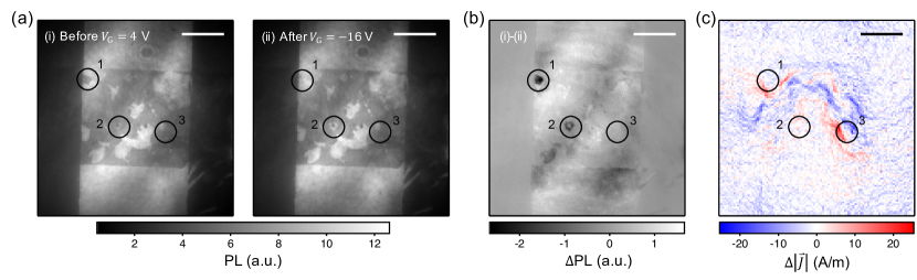
The current density maps produced by this method showed differing density distributions at each doping condition [Fig. 2]. A simple explanation for these differences is that they are due to degradation of the graphene throughout the measurement, which was often observed following sustained high source-drain currents ( A) and at high gate potentials ( V). To determine whether the observed differences arise from significant tearing of the graphene or not, we compare PL images of the device taken under the same conditions prior to mapping at V, and after mapping at V [Fig. 8(a)]. A subtraction of these two PL images highlights two regions (marked and ) in the gated section of the graphene ribbon where the graphene is no longer visible via FRET interaction with the NV-layer in the later measurement [Fig. 8(b)]. PL imaging between the two current measurements indicate that these changes occurred during the V measurement. The fringes visible across the device in the subtraction are due to a slight shift in the optics between measurements.
Comparing the PL subtraction to the current density subtraction [Fig. 8(c)] shows that there is a deviation in current path close to one of the tears (). Interestingly, the region showing the most distinct change in current path (marked ) shows very little PL change, indicating that it is not associated with a degradation of the graphene visible at our imaging resolution. Further investigation into the cause of this current deviation is made difficult by the gradual deterioration of the device throughout measurement, which precludes repeat measurements, and motivates a new generation of devices which better isolate the graphene from the diamond substrate and oxide-interface.
Appendix E Electric field simulations
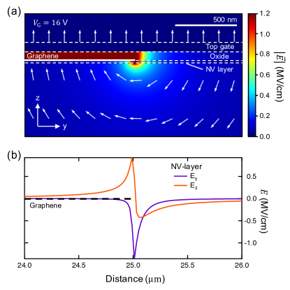
To determine the spatial distribution of the electric field from the top gate, such that it can be compared to that measured by the NV-layer, a finite element method (FEM) simulation was performed using COMSOL. The device geometry was replicated, where a m wide metallic top gate was separated from a graphene ribbon by nm of Al2O3, all hosted on top of a m thick diamond substrate. The electric field distribution was calculated in a shell surrounding the device, using a high density mesh in the region of interest between the metallic planes and beneath the graphene plane, across the region containing the NV-layer.
The simulated electric field shows a high field strength between the parallel plate capacitor ( MV/cm in the centre of oxide), which is screened from the diamond by the graphene plate [Fig. 9(a)]. Appreciable field strengths exist in the diamond only at the edge of the graphene ribbon under the top gate, where the magnitude reaches MV/cm in the z-direction, but reverses in sign within a nm length scale across the graphene ribbon edge [Fig. 9(b)]. The component perpendicular to the graphene ribbon reaches MV/cm at the edge, but is laterally confined to nm. Given the optical resolution limited imaging via the NV-layer PL, we do not expect to be able to resolve these features, and hence conclude that the NV-layer measurements should not be sensitive to electric field from the gate directly. Therefore, we propose that the enhanced electric field we measured, which correlates strongly with the gate potential dependent PL effect, must result from a change in the surface charge distribution at the diamond-oxide interface.