Spin-momentum locked modes on anti-phase boundaries in photonic crystals
Abstract
An anti-phase boundary is formed by shifting a portion of photonic crystal lattice along the direction of periodicity. A spinning magnetic dipole is applied to excite edge modes on the anti-phase boundary. We show the unidirectional propagation of the edge modes which is also known as spin-momentum locking. Band inversion of the edge modes is discovered when we sweep the geometrical parameters, which leads to a change in the propagation direction. Also, an optimized source is applied to excite the unidirectional edge mode with high directivity.
Keywords Spin-momentum locking Anti-phase boundary Photonic crystal waveguides
1 Introduction
The quantum spin-Hall effect indicates that the spin of the electron is locked to the direction of propagation [1]. The index, or the spin Chern number which is a topological invariant of the given quantum system is defined to verify if the spin Hall conductance exists on the edge of the bulk material [2, 3]. After introducing the topological index to analyze the system, a variety of unidirectional edge modes in quantum systems were discovered [4, 5, 6]. By analogy with the quantum spin-Hall effect of electrons, spin-momentum locking phenomena can also be found in photonic topological insulators [7, 8, 9, 10, 11]. The direction of propagation is still used to define ’momentum’ of the light while the concept of ’spin’ is not as clear as the spin of the electron. It may refer to the bonding (antibonding) states of electric and magnetic fields [7], left-hand (right-hand) circular polarizations of electric fields [8], and clockwise (anticlockwise) circulations of coupled resonator optical waveguides [11].
Spin-momentum locked edge modes can also be discovered in trivial optical systems without topological properties, such as photonic crystal waveguides [12, 13, 14], surface plasmon polaritons [15, 16], and even dielectric waveguides [16]. A pair of orthogonal dipoles with phase differences which represent opposite spin directions are applied to excite the unidirectional edge modes in these systems. The spin of dipole sources couples to the spin of evanescent waves near the edges, giving rise to the spin-momentum locked edge modes.
An anti-phase boundary is created by shifting the crystal by one-half period along the propagation direction. It can be observed in electronic systems and can be treated as a defect in the crystal that breaks the translation symmetry [17, 18]. Accurate atomic manipulation is required in order to design the anti-phase boundaries in electronic systems [19, 20]. It is easier to design the anti-phase boundary in photonic system, which may help us have a deeper understanding of how the energy is distributed near the anti-phase boundary.
In this paper, we create an anti-phase boundary in a photonic crystal structure by shifting the structure along the direction of periodicity. Unidirectional propagation of the edge modes is discovered. To the authors’ best knowledge, spin-momentum locked edge modes have not been found on anti-phase boundaries in quantum or optical systems. It will not only make the existence of the propagating edge modes along anti-phase boundaries in quantum systems possible, but also provide a new way to design chiral waveguides in photonic crystal structures.

2 Spin-momentum locked modes

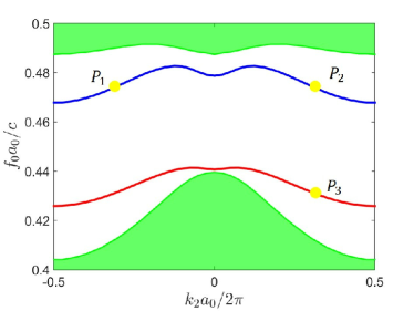
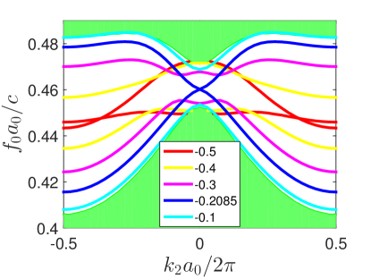
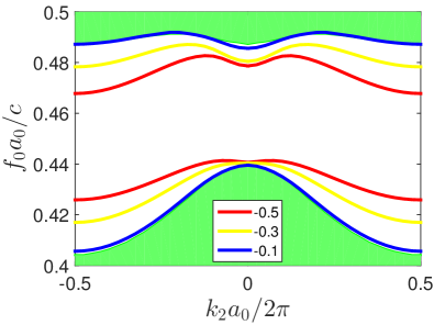
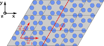
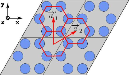
As shown in Fig. 1, an anti-phase boundary is created by shifting the photonic crystal along the direction by , which is one-half period. The geometry and material parameters are given in Fig. 1. Here we only investigate the transverse magnetic (TM) modes of the electromagnetic waves, where only , , and are nonzero. According to Ref. [8], tuning the distance between the center of the diamond and the center of cylinders will change the topological properties of the crystal. When , the structure behaves as a topologically trivial material with index equal to zero. Band folding occurs when since the lattice vectors of the unit cell change into and as shown in Fig. 2. The size of the unit cell shrinks while the Brillouin zone expands. If the original Brillouin zone () is chosen, the bands on expanded Brillouin zone () must be folded to fit in the original one, which leads to the creation of a Dirac cone at the point. Further increasing opens the band gap at point and turns the trivial crystal into a topological insulator with nonzero index. Band inversion happens at the point when with dipole modes in the higher band and quadrupole modes in the lower band. Unidirectional edge modes can be found at the boundary between the topological insulator () and trivial crystal ().
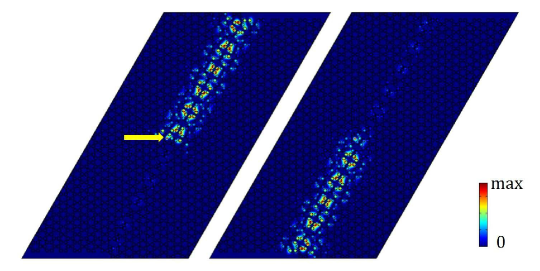
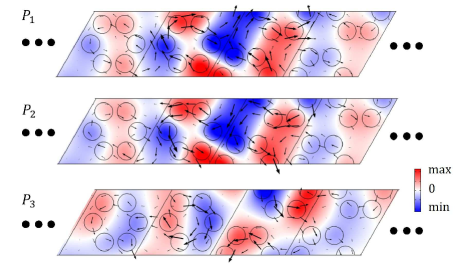
Here we place the topological insulator with on both sides of the boundary as shown in Fig. 1b. However, the topological properties of the photonic crystal cannot explain the edge modes discovered on the anti-phase boundary since shifting will not change the band diagram and index of the crystal. As shown in Fig. 3a, the odd edge modes (anti-symmetric distributions) and the even edge modes (symmetric distributions) are caused by the mirror symmetry of the super-cell. The field distributions of the edge modes calculated by COMSOL are given in Fig. 3b. The distributions at point and defined in Fig. 3a are the same while the Poynting vectors are in opposite directions. Here we define the counter clockwise rotation of the Poynting vectors on the left side of the anti-phase boundary as spin-up and the clockwise rotation as spin-down. By comparing and we know that the edge modes with the same frequency but opposite k vectors have different spin directions. Also, we show that the edge modes with the same k vector have opposite spin directions by comparing the fields at and .
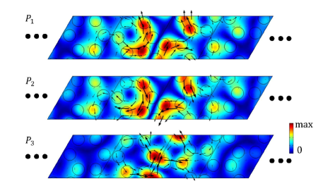
In order to excite the edge modes, a circularly polarized magnetic dipole is chosen as the source in our driven mode simulation. By observing the Poynting vectors in Fig. 3c, we conclude that magnetic dipole behaves like the spin-up source while like the spin-down source. The frequency of excitation is chosen to be inside the band gap of the bulk modes, which only excite the odd edge modes as we can conclude from Fig. 3a. We apply the spin-up source to the shifted structure to excite the spin-up edge mode at . Since the group velocity at is positive, the wave will propagate along the direction . The simulation result shown on the left side of Fig. 3d matches this theoretical prediction. Similarly, a spin-down source will excite the edge mode propagates along , which is also shown on the right side of Fig. 3d.
Tuning the parameter to will dramatically change the properties of the edge modes. According to Ref. [8], the band diagram has been closed and reopened at the point when tuning the from to . The even edge mode rises while the odd mode declines. As shown in Fig. 4a, the even mode is above the odd mode inside the band gap when , which is opposite to the result shown in Fig. 3a. If we apply the spin-up source with normalized frequency inside the band gap, it will excite the spin-up edge mode at as shown in Fig. 4b. Since the group velocity at is negative, the wave will propagate along the direction, which is verified by the left part of Fig. 4c. This indicates both topological and trivial photonic system can form anti-phase boundary and support spin-momentum locked edge modes on the boundary. The source of the same spin can excite wave with opposite propagation directions in these two photonic crystal systems.
3 Band inversion of edge modes when tuning the offset
By tuning the offset which is defined in Fig. 1b, we can get a series of dispersion relations as shown in Fig. 5a and Fig. 5b. Since the mirror symmetry is broken for , we can’t define the odd mode or even mode according to the mirror plane. For the trivial unit cell, varying from the anti-phase boundary with to the two dimensional photonic crystal with will make the dispersion curve get closer to the projected bulk band diagram. The variation of dispersion curves for the structure consisting of topological unit cell is more complicated. As shown in Fig. 5a, the two dispersion curves converge at the point and form a degenerate point at when the offset . If we continue changing from to , the gap between two edge modes reopens and increases until the two curves vanish into the bulk bands.
The band inversion occurs at the point when the offset crosses over the degenerate case . As shown in Fig. 5c, the distributions in the higher band of the case are the same as the lower band when . When is sufficiently far away from the point, the field distributions look similar in the higher band or lower band for different offsets. We can conclude that only the edge modes that are close to point will be inverted when , which is similar to the band inversion of the bulk modes in Ref. [8].
4 Edge modes in gradual shift structure
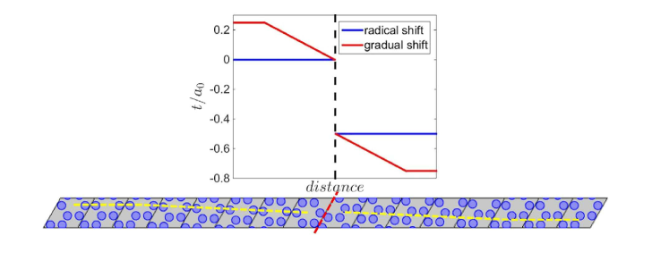

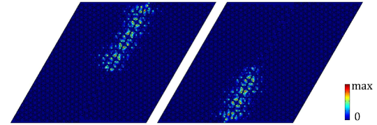
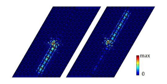
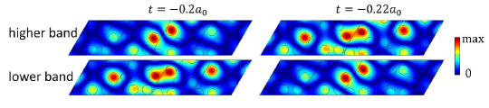
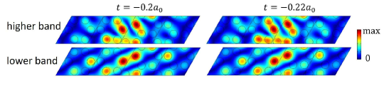
We can also create an anti-phase boundary by gradually shifting the unit cells on the two sides of the boundary as shown in Fig. 6a. Here the unit cell with is studied. We can conclude from the dispersion relations shown in Fig. 5a that the edge modes which decay rapidly into the bulk can only be found when the offset between the adjacent unit cells is large enough. For the offset with , the dispersion curves are so close to the bulk band diagram that their energy is not well confined to the boundary. Hence the offset of is chosen between the adjacent unit cells on the two sides of the anti-phase boundary to prevent the appearance of redundant edge modes. The unit cells will look the same if they are far enough from the boundary, which is different from the radical shift structure where the offset difference always exists on the two sides. In this structure, there is no long-range offset between the two sides, only a local shift in the unit cells near the boundary. The dispersion relation and field distribution are shown in Fig. 6b and Fig. 6c respectively, which is similar to the radical shift case as shown in Fig. 3a and Fig. 3b. The unidirectional propagation of the edge modes can also be found when we excite with sources of different spin directions as shown in Fig. 6d.
5 Optimization of the source
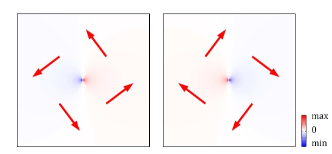
By optimizing the combination of two orthogonal magnetic dipoles, we can achieve edge modes with better directionality. The magnetic dipole can be defined as:
| (1) |
where and . The spin-up () and spin-down () source mentioned above are the particular cases when and in Eq. 1 are set to and respectively.
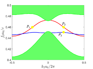
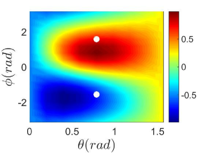
According to Ref. [21], we can also define the directionality of the edge mode by
| (2) |
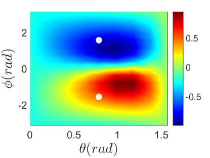
where () is the line integration of the Poynting vector measured on the top(bottom) of the structure as shown in Fig. 4c. If is close to 1, we can conclude that the system has good directionality while no directionality can be observed when . As shown in Fig. 7, the signs of at the locations of spin-up and spin-down source are opposite for and , which verifies the conclusion that wave propagates in opposite directions for the same source when we tune the of the system.
6 Conclusion
Spin-momentum locked edge modes are discovered on the anti-phase boundaries which are formed by shifting two halves of a photonic crystal along the direction of periodicity. By applying magnetic dipole sources with different spin directions, we can excite the edge modes propagating in opposite directions. The inversion of the edge modes is revealed when we adjust the distance between the center of the unit cell and the cylinders, which leads to opposite propagation directions with the same source. Also, tuning the offset of the unit cells on two sides can cause band inversion of the edge modes for the topologically non-trivial photonic crystal system. Optimization of the source gives the edge modes better directionality and helps us to further understand the system, making it more practical for the unidirectional wave propagation applications.
Acknowledgments
This work was supported in part by Air Force Office of Scientific Research Grant No. FA9550-16-1-0093 and in part by the China Scholarship Council (No. 201706230113). The authors acknowledge discussions with D. Bisharat.
References
- [1] Charles L Kane and Eugene J Mele. Quantum spin hall effect in graphene. Physical review letters, 95(22):226801, 2005.
- [2] Charles L Kane and Eugene J Mele. Z 2 topological order and the quantum spin hall effect. Physical review letters, 95(14):146802, 2005.
- [3] DN Sheng, ZY Weng, L Sheng, and FDM Haldane. Quantum spin-hall effect and topologically invariant chern numbers. Physical review letters, 97(3):036808, 2006.
- [4] Markus König, Hartmut Buhmann, Laurens W. Molenkamp, Taylor Hughes, Chao-Xing Liu, Xiao-Liang Qi, and Shou-Cheng Zhang. The quantum spin hall effect: theory and experiment. Journal of the Physical Society of Japan, 77(3):031007, 2008.
- [5] Ferdinand Kuemmeth, S Ilani, DC Ralph, and PL McEuen. Coupling of spin and orbital motion of electrons in carbon nanotubes. Nature, 452(7186):448, 2008.
- [6] Anjan Soumyanarayanan, Nicolas Reyren, Albert Fert, and Christos Panagopoulos. Emergent phenomena induced by spin–orbit coupling at surfaces and interfaces. Nature, 539(7630):509, 2016.
- [7] Alexander B Khanikaev, S Hossein Mousavi, Wang-Kong Tse, Mehdi Kargarian, Allan H MacDonald, and Gennady Shvets. Photonic topological insulators. Nature materials, 12(3):233, 2013.
- [8] Long-Hua Wu and Xiao Hu. Scheme for achieving a topological photonic crystal by using dielectric material. Physical review letters, 114(22):223901, 2015.
- [9] Tzuhsuan Ma and Gennady Shvets. Scattering-free edge states between heterogeneous photonic topological insulators. Physical Review B, 95(16):165102, 2017.
- [10] Tomoki Ozawa, Hannah M Price, Alberto Amo, Nathan Goldman, Mohammad Hafezi, Ling Lu, Mikael C Rechtsman, David Schuster, Jonathan Simon, Oded Zilberberg, et al. Topological photonics. Reviews of Modern Physics, 91(1):015006, 2019.
- [11] Mohammad Hafezi, Eugene A Demler, Mikhail D Lukin, and Jacob M Taylor. Robust optical delay lines with topological protection. Nature Physics, 7(11):907, 2011.
- [12] Immo Söllner, Sahand Mahmoodian, Sofie Lindskov Hansen, Leonardo Midolo, Alisa Javadi, Gabija Kiršanskė, Tommaso Pregnolato, Haitham El-Ella, Eun Hye Lee, Jin Dong Song, et al. Deterministic photon–emitter coupling in chiral photonic circuits. Nature nanotechnology, 10(9):775, 2015.
- [13] RJ Coles, DM Price, JE Dixon, B Royall, E Clarke, P Kok, MS Skolnick, AM Fox, and MN Makhonin. Chirality of nanophotonic waveguide with embedded quantum emitter for unidirectional spin transfer. Nature communications, 7:11183, 2016.
- [14] Andrew B Young, ACT Thijssen, Daryl M Beggs, Petros Androvitsaneas, L Kuipers, John G Rarity, Stephen Hughes, and Ruth Oulton. Polarization engineering in photonic crystal waveguides for spin-photon entanglers. Physical review letters, 115(15):153901, 2015.
- [15] Todd Van Mechelen and Zubin Jacob. Universal spin-momentum locking of evanescent waves. Optica, 3(2):118–126, 2016.
- [16] Francisco J Rodríguez-Fortuño, Giuseppe Marino, Pavel Ginzburg, Daniel O’Connor, Alejandro Martínez, Gregory A Wurtz, and Anatoly V Zayats. Near-field interference for the unidirectional excitation of electromagnetic guided modes. Science, 340(6130):328–330, 2013.
- [17] D Cohen and CB Carter. Structure of the (110) antiphase boundary in gallium phosphide. Journal of microscopy, 208(2):84–99, 2002.
- [18] KH Ahn, T Lookman, A Saxena, and AR Bishop. Electronic properties of structural twin and antiphase boundaries in materials with strong electron-lattice couplings. Physical Review B, 71(21):212102, 2005.
- [19] Zhen Wang, Hangwen Guo, Shuai Shao, Mohammad Saghayezhian, Jun Li, Rosalba Fittipaldi, Antonio Vecchione, Prahald Siwakoti, Yimei Zhu, Jiandi Zhang, et al. Designing antiphase boundaries by atomic control of heterointerfaces. Proceedings of the National Academy of Sciences, 115(38):9485–9490, 2018.
- [20] Xian-Kui Wei, Alexander K Tagantsev, Alexander Kvasov, Krystian Roleder, Chun-Lin Jia, and Nava Setter. Ferroelectric translational antiphase boundaries in nonpolar materials. Nature communications, 5:3031, 2014.
- [21] Jan Petersen, Jürgen Volz, and Arno Rauschenbeutel. Chiral nanophotonic waveguide interface based on spin-orbit interaction of light. Science, 346(6205):67–71, 2014.