Also at ]Institute of Semiconductor Electronics (IHT), RWTH Aachen University, 52074 Aachen, Germany Also at ]Integrated Materials Design Lab (IMDL), The Australian National University, ACT 2601, Australia
Electronic Structure Shift of Deep Nanoscale Silicon by SiO2- vs. Si3N4-Embedding as Alternative to Impurity Doping
Abstract
Conventional impurity doping of deep nanoscale silicon (dns-Si) used in ultra large scale integration (ULSI) faces serious challenges below the 14 nm technology node. We report on a new fundamental effect in theory and experiment, namely the electronic structure of dns-Si experiencing energy offsets of ca. 1 eV as a function of SiO2- vs. Si3N4-embedding with a few monolayers (MLs). An interface charge transfer (ICT) from dns-Si specific to the anion type of the dielectric is at the core of this effect and arguably nested in quantum-chemical properties of oxygen (O) and nitrogen (N) vs. Si. We investigate the size up to which this energy offset defines the electronic structure of dns-Si by density functional theory (DFT), considering interface orientation, embedding layer thickness, and approximants featuring two Si nanocrystals (NCs); one embedded in SiO2 and the other in Si3N4. Working with synchrotron ultraviolet photoelectron spectroscopy (UPS), we use SiO2- vs. Si3N4-embedded Si nanowells (NWells) to obtain their energy of the top valence band states. These results confirm our theoretical findings and gauge an analytic model for projecting maximum dns-Si sizes for NCs, nanowires (NWires) and NWells where the energy offset reaches full scale, yielding to a clear preference for electrons or holes as majority carriers in dns-Si. Our findings can replace impurity doping for n/p-type dns-Si as used in ultra-low power electronics and ULSI, eliminating dopant-related issues such as inelastic carrier scattering, thermal ionization, clustering, out-diffusion and defect generation. As far as majority carrier preference is concerned, the elimination of those issues effectively shifts the lower size limit of Si-based ULSI devices to the crystalization limit of Si of ca. 1.5 nm and enables them to work also under cryogenic conditions.
I Introduction
Impurity doping of Si has been a prerequisite for Si-based electronics for about 70 years Pearson and Bardeen (1949). Over the last decade, impurity doping gradually became a major issue in ultra-large scale integration (ULSI) as fin/nanowire (NWire) device features approached the characteristic lengths of dopant out-diffusion, clustering and inactivation Koelling et al. (2013). Considerable broadening of dopant profiles from drain/source regions into gate areas persists even when using self-regulatory plasma doping combined with rapid spike annealing Kambham et al. (2013). To add, required ULSI transistor functionality Duffy et al. (2018) and emerging applications of Si-nanocrystals (NCs) Heitmann et al. (2005) unveiled additional doping issues such as self-purification Dalpian and Chelikowsky (2006); Stegner et al. (2009), dopant ionization failing at room temperature Chan et al. (2008); König et al. (2015) and dopant-associated defect states Pereira et al. (2012); König et al. (2015); Hiller et al. (2017, 2018a).
In the late 1970s, modulation doping of III-V semiconductor combinations such as GaAs/AlAs was discovered Dingle et al. (1978). Lately, this concept was applied successfully to Si by acceptor doping of adjacent SiO2 König et al. (2017); Hiller et al. (2018b); König et al. (2018a) and proposed for donor-doping AlxGa1-xN barriers from adjacent Si-rich Si3N4 during Si-NC formation anneal König and Rudd (2013).
Ideally, majority carrier preference for electrons/holes and thus n/p-type conductivity would not require doping if the electronic structure of deep nanoscale Si (dns-Si) could be shifted over energy as per n/p-type section of an electronic device. Such an energy offset would avoid all dopant-related issues mentioned above, leading to lower inelastic carrier scattering rates and higher carrier mobilities which allow for decreased heat loss and bias voltages in ULSI. Together with directed self-assembly of block copolymers as new lithography approach to dns-Si structures Liu et al. (2018), such properties enable Si-FET technology to work at yet smaller structure sizes potentially enabling Moore’s Law to approach the Si-crystallization limit of ca. 1.5 nm Schuppler et al. (1994). In a recent paper König et al. (2018b) we were able to demonstrate in theory and experiment that exists in dns-Si when embedding one part of the Si nanovolume in SiO2 and another part in Si3N4. However, a detailed investigation of the impact originating from interface bond densities per square, thickness of embedding dielectric and sample size on the magnitude of the effect is missing. The latter is very important for the applicability of the effect in real devices. As an effect induced via the interface of dns-Si, the extension of the p/n-junction is on the order of ca. 15 Å, allowing for a leap in device miniaturization. Moreover, we deliver a detailed phenomenologial description of the fundamental quantum-chemical origin of which is underpinned by experimental data and DFT results.
In our work presented here, we consider SiO2- and Si3N4-embedding of Si-NCs as a function of shape, size, interface orientation and thickness of embedding dielectric by using density functional theory (DFT) to calculate their electronic structure. As the next step, we compute DFT approximants containing two NCs, one embedded in SiO2 and the other in Si3N4, to verify the we found for single Si-NCs within one system, accounting for interactions of both Si-NCs. From there, we present experimental data on Si-nanowells (NWells) embedded in SiO2 vs. Si3N4, namely information on the ionization energy of the valence band edge of the Si-NWells by long-term synchrotron ultraviolet photoelectron spectroscopy (UPS)Berglund and Spicer (1964, 1999); Reinert and Hüfner (2005); Suga and Sekiyama (2014); König et al. (2018b, c). With this wealth of theoretical and experimental data, we propose a model explaining the interface impact of oxygen (O) and nitrogen (N) onto dns-Si, the associated characteristic impact length and other prominent features observed in the electronic structure of dns-Si. The massive observed in theory and experiment presents a new fundamental effect which can replace doping by forcing dns-Si into p- or n-type carrier preference as a function of embedding dielectric. Thereby, advantages of fully depleted field effect transistor (FET) ULSI devices can be combined with carrier preferences hitherto only achieved by impurity doping.
II Methods
II.1 Density Functional Theory Calculations
Hybrid density functional theory (h-DFT) calculations were carried out in real space with a molecular orbital basis set (MO-BS) and both Hartree-Fock (HF) and h-DFT methods as described below, employing the Gaussian09 program suite G09 (2010). Initially, the MO-BS wavefunction ensemble was tested and optimized for stability with respect to describing the energy minimum of the approximant (variational principle; ) with the HF method using a 3-21G MO-BS Gordon et al. (1982) (HF/3-21G). This MO wavefunction ensemble was then used for the structural optimization of the approximant to arrive at its most stable configuration (maximum integral over all bond energies), again following the HF/3-21G route. Using these optimized geometries, their electronic structure was calculated again by testing and optimizing the MO-BS wavefunction ensemble with the B3LYP hybrid DF Becke (1988); Lee et al. (1988) and the 6-31G(d) MO-BS Francl et al. (1982) (B3LYP/6-31G(d) ). Root mean square (RMS) and peak force convergence limits were 8 meV/Å and 12 meV/Å, respectively. Tight convergence criteria were applied to the self-consistent field routine. Ultrafine integration grids were used throughout. During all calculations, no symmetry constraints were applied to MOs. Extensive accuracy evaluations can be found elsewhere König et al. (2008, 2014, 2018c). We note that in real-space DFT calculations, exact calibration to an absolute energy scale (the vacuum level ) is known to be ambiguous Rissner et al. (2011). Nevertheless, relative changes of energy values such as or fundamental energy gaps between approximants with different interface termination are accurate within the same computation route, leaving a constant energy shift to all states with respect to as the only uncertainty. Approximants and MOs were visualized with Gview 5 Dennington et al. (2009). Electronic density of states (DOS) were calculated from MO eigenenergies, applying a Gaussian broadening of 0.2 eV. The sizes given for NCs were calculated as the product of atomic volume of Si and the number of Si atoms forming the NC, assuming a spherical shape. This approach allows for a direct comparison of results between approximants of different shape.
II.2 Sample Preparation
Samples comprising a Si3N4-embedded NWell were fabricated by plasma enhanced chemical vapour deposition (PECVD) using SiHNHN2 for Si3N4 buffer and top layers (thickness 5.5 and 1.5 nm, respectively) and SiH Ar for amorphous Si Hiller et al. (2014). The Si3N4 spacer layer served to suppress excited electrons from the Si wafer to interfere with electrons from the Si-NWell during UPS. The substrates, i. e. n-type Si wafers (Sb doping, to cm) of (111)-surface orientation, were wet-chemically cleaned. After deposition the wafers were annealed in a quartz tube furnace for 1 min at C in pure N2 ambient to induce Si-crystallization. Subsequently, samples were H2-passivated at C for 1 hour.
Samples comprising a SiO2-embedded NWell were dry-etched with an isotropic SF6/O2 plasma to thin down a 85 nm thick top c-Si layer of an Si-on-insulator (SOI) wafer with 200 nm buried SiO2 (BOX), arriving at ca. 2.7 to 6.5 nm thick c-Si on top. The back-etch was followed by oxidation in 68 wt-% HNO3 at 120 ∘C, resulting in a 1.1 to 5.0 nm Si-NWell with 1.4 nm SiO2 capping.
Si reference samples were processed by etching a 001-Si wafer (Sb-doped n-type, to cm) in 1 wt-% buffered hydrofluoric acid and immediate sample mounting under a N2-shower with swift loading into the ultra-high vacuum (UHV) annealing chamber.
All NWell samples were contacted via a lateral metal contact frame on the front surface which was processed by photolithographical structuring, wet-chemical etching in 50 % HF plus 0.1 % HNO3 for opening the top Si3N4 or in 1 wt-% hydrofluoric acid for opening the top SiO2 layer and thermal evaporation of 300 nm Al, followed by a lift-off in dimethyl-sulfoxide (). The Si reference samples were contacted directly on their front surface. Fig. 1 shows the structure of the mesa samples.
(a) (b)
II.3 Characterization
Ultraviolet photoelectron spectroscopy (UPS) measurements were carried out at the BaDElPh beamline Petaccia et al. (2009) at the Elettra Synchrotron in Trieste, Italy, see König et al. (2018b) for details. All samples were subject to a UHV anneal for 90 min at 500 K to desorb water and air-related species from the sample surface prior to measurements. Single scans of spectra were recorded over 12 h per NWell sample and sub-sequently added up for eliminating white noise. Scans for the Si-reference sample were recorded over 2 h and sub-sequently added up König et al. (2018b). All samples of beamtime 1 were exited with photon energies of eV and a photon flux of s-1. Samples of beamtime 2 were excited with eV and a photon flux of s-1, yielding to slightly better signal-to-noise ratio (SNR) due to an increased inelastic mean free path of escaping electrons. The incident angle of the UV beam onto the sample was 50∘ with respect to the sample surface normal, excited electrons were collected with an electron analyzer along the normal vector of the sample surface. Energy calibration of the UPS was realized using a tantalum (Ta) stripe in electrical contact to the sample as a work function reference. Further UPS-data of SiO2 and Si3N4 reference samples as well as on UPS signal normalization and background substraction are available in König et al. (2018b, c) and in Appendix Sec. A.
All samples for transmission electron microscopy (TEM) investigation were capped with a protective 100 nm thick SiO2-layer to facilitate the preparation of cross sections by the focused ion beam (FIB) technique using a FEI Strata FIB 205 workstation. Some samples were further thinned by means of a Fischione NanoMill. TEM analysis of the cross sections was performed at a FEI Tecnai F20 TEM operated at 200 kV at the Central Facility for Electron Microscopy, RWTH Aachen University, and at the spherical aberration corrected FEI Titan 80-300 TEM operated at 300 kV at Ernst Ruska-Centre, Forschungszentrum Jülich Thust et al. (2016).
In addition, Si-NWell thicknesses were measured by ellipsometry. The thickness of Si-NWells in Si3N4 and in SiO2 were measured using a Woollam M-2000 ellipsometer and an ACCURION nanofilm ep4se ellipsometer, respectively. All thickness measurements were confirmed by values obtained from TEM. Yet, samples were given a standard deviation in NWell thickness of monolayer (ML) due to the large extension of the measurement spot during UPS as compared to NWell thickness.
III DFT Results
III.1 Single Si-NCs coated with SiO2 vs. Si3N4
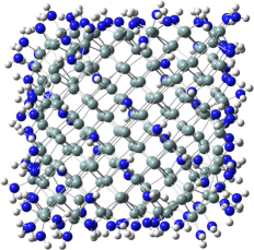
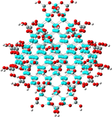
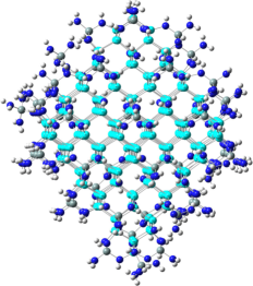
With the interface charge transfer (ICT) at the core of , we investigate the nature of the interface and the interface-to-volume ratio of dns-Si as key parameters defined by system size. The latter can be expressed by the ratio of interface bonds to the number of Si-NC atoms König (2016), whereby this ratio can be applied to other dns-Si volumes such as NWires or fins König and Smith (2019). Apart from its termination with OH- vs. NH2-groups, the nature of the interface is defined by its orientation with characteristic bond densities per square. We choose the - and -orientations with their interface bond densities per cm2 of cm-2 and cm-2 Hesketh et al. (1993), respectively, for two reasons. First, the technologically most relevant interface orientations of dns-Si are , and . Second, cm-2 for -orientations of Si interfaces Hesketh et al. (1993) is close to whereby a significant difference of its impact onto the ICT is not given. We calculated octahedral approximants with exclusive -orientations up to Å – Si455X196 with X OH, NH2, see Fig. 2a – and cubic approximants with exclusive -orientations and associated bridge bonds () of NH- and O-groups up to Å – Si216(XH-1)75X48 with XH O/NH, see Fig. 2b. Computations of bigger cubic NCs such as Si512(XH-1)75X48 were not successful due to excessive strain induced by NH and in particular O disintegrating the cubic shape.
(a)
(b)
(c)
Another important parameter is the thickness of the embedding dielectric. We calculated octahedral Si-NCs with exclusive -orientations as above, but covered in 1.5 ML SiO2 or Si3N4 up to Si286 NCs ( Å). Thereby, we can directly compare the electronic structure of both approximant cohorts. Fig 2c shows such approximants where the NCs have been highlighted.
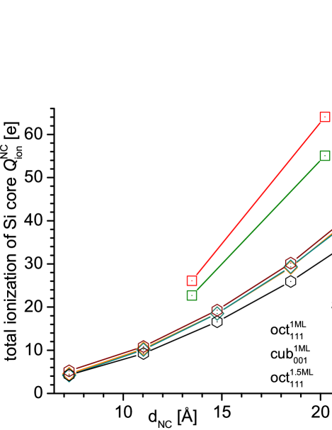
We now focus on the ionization of Si-NCs, see Fig. 3. It provides a blueprint of the strength of the ICT which is closely linked to . All total NC ionizations over show a quadratic dependence which clearly points to a surface effect König et al. (2014); König (2016). In general, O-terminated species have a slightly higher ionization although the difference in ionicity of the bond Si—O with ca. 53 % ionic vs. Si—N with ca. 35 % is significant Holleman et al. (1995); König et al. (2008). The minute difference for OH-/NH2-terminated octahedral NCs shows that the ICT is saturated for Å. As we will see in Sec. V, this value is merely limited by tractable DFT system size and surpassed roughly 3-fold when feeding experimental results into an analytic impact model of König et al. (2014). Accordingly, the embedding of Si-NCs into 1.5 ML SiO2 does only yield to a slightly higher , whereby ionization drops notably for coating in 1.5 ML Si3N4. The origin of the latter is due to the positive electron affinity of N which deflects the valence electron wavefunctions originating from Si-NC atoms back into the NC, resulting in a delocalization of these wavefunctions, see Sec. V for details. Due to MO hybridization, the unoccupied states follow suit. Considering as a function of interface orientation, it becomes apparent that -faceted interfaces with their increased bond density yield a stronger ICT. A direct comparison of between -cubic vs. -octahedral NCs cannot be accomplished due to their different . As a good estimate, we can compare the average value of the Si165X100 and Si286X144 NCs of with their average size of Å to of the -cubic approximant Si216(XH-1)75X48 with Å König (2016). We thus arrive at of the number of interface bonds per NC atom when going from -octahedral to -cubic NCs. Accordingly, -cubic NCs are significantly more ionized than -octahedral NCs which can be seen in Fig. 3.
Alternations of the ICT as function of interface orientation and thickness of embedding dielectric result in a modification of the NC electronic structure, namely energies of the highest occupied MO (HOMO) and of the lowest unoccupied MO (LUMO) , see Fig. 4.
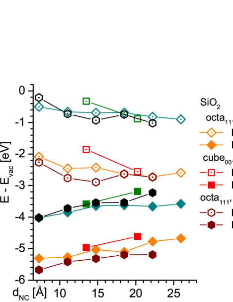
The increased ICT due to a higher ratio for -cubic NCs or by increasing the dielectric embedding from 1 to 1.5 ML results in a more pronounced shift with respect to the vacuum level . For N-terminated NCs, a more pronounced shift towards is clearly visible for the -octahedral NCs embedded in 1.5 ML Si3N4 and in particular for the -cubic NCs. The results for O-terminated -octahedral NCs show the same trend with more pronounced shifts further below . The cubic NCs Si64(O)27(OH)30 ( Å) and Si216(O)75(OH)48 do not follow the trend which appears surprising on a first glance. When looking at the latter cubic Si-NC (see Fig. 2b), it becomes apparent that considerable strain deforms the NC cube. For -octahedral NCs, strain has only a minor influence on their electronic structure even with embedding – see Fig 2 and König et al. (2018b). However, with many O bond configurations on interfaces, strain may become more influential on the electronic structure. Such strain becomes evident when comparing bond lengths and angles as listed in Table 1. The bond length of O—Si bonds in ultrathin SiO2 at the NC is ca. 7.4 % longer when compared to SiO2, while the value for Si—N bonds is only stretched by ca. 3.8 % with respect to Si3N4 König et al. (2018c). A similar situation exists with bond angles of Si atoms when going from the NC center to its interface. Together with a bond energy of eV vs. eV Holleman et al. (1995), the combination of higher and shorter bond lengths shows that O bond configurations to Si are capable of generating notably more local strain as opposed to NH bond configurations. With O-terminated -cubic NCs, it appears that significant strain lowers the binding energy of the system which is reflected in a slight shift towards , see Fig. 4. It was reported that strain dominates the electronic structure of even -octahedral Si-NCs embedded in SiO2 Guerra et al. (2009), although we cannot confirm such results with own calculations of such Si-NCs in up to 3 ML of SiO2 König et al. (2018b). Hence, only massive strain emerges as modifier to the electronic structure, though still exceeded considerably by the impact of embedding dielectric via ICT. Bigger -cubic approximants such as Si512(O)147(OH)66 with Å get partially disintegrated by strain due to O bonds, showing that stress destroys the NC before becoming dominant over the ICT.
In summary, we observed a substantial energy offset of the electronic structure of Si-NCs terminated with O vs. N, yielding to eV and eV with 1.5 ML coating by SiO2 vs. Si3N4. These values correspond to ca. 75 % and 55 %, respectively, of the nominal HOMO-LUMO gap of Si-NCs in the size range of 20 Å. We found that the ICT is dominated by bond densities per square given by interface orientation via the ratio and to a lesser degree by the thickness of the embedding dielectric. Interface strain originating from O bonds does have a minor influence on the electronic structure by decreasing binding energies of -cubic NCs, shifting their electronic structure slightly towards , opposing the downshift of the electronic structure by SiO2-embedding to some extent.
III.2 One Approximant Featuring a Si-NC in SiO2 Adjacent to a Si-NC in Si3N4
An approximant consisting of two Si-NCs, with the first (second) NC embedded in SiO2 (Si3N4), presents the ultimate DFT system to test the energy offset and to gain further insight into its working principle. We calculated four approximants which mainly differ in the size of embedded Si-NCs: Si10 (7.2 Å each) König et al. (2018b), Si35 (11.0 Å each), Si84 (14.8 Å each) and Si165 (18.5 Å each). The latter two NC sizes overlap with experimental observations, thus providing a solid ground for Sec. V where we estimate the size range up to which dns-Si systems are dominated by .
Fig. 5 shows the results for the Si35, Si84 and Si165 approximants, with respective DOS ranges enlarged to show the localization of the electronic states within the approximants. Underneath these DOS ranges, iso-density plots of the partial DOS located dominantly within one of the NCs are shown as a function of their embedding.
We can clearly see two effects: and increase with NC separation growing with NC size 111There are 2 ML, 3 ML, 4 ML and 4.5 ML of SiO2 plus Si3N4 for the Si10-, Si35-, Si84- and Si165-approximants separating the NCs. Increasing inter-NC layer thickness of the combined dielectrics or thickness of the dielectric at outer NC facets is not possible at present due to intractability of DFT computations for heavy atoms with the level of theory we use.. The global energy gap of the entire approximant decreases with NC size. Both effects lead to a superlinear increase in n/p-type preference for charge carriers with increasing NC size, cf. Fig. 6, and in general with the size of dns-Si systems up to a certain limit, see Sec. V. We note that and of the Sin approximants () do not reach the values obtained for individual NCs in Sec. III.1. The proximity of SiO2 to Si3N4 results in a transient region where the electron-localizing nature of O cancels out with the electron-delocalizing nature of N König et al. (2018b). Since the combined thickness of SiO2 and Si3N4 between NCs gets thicker with increasing NC size, this effect diminishes to yield to increased and .
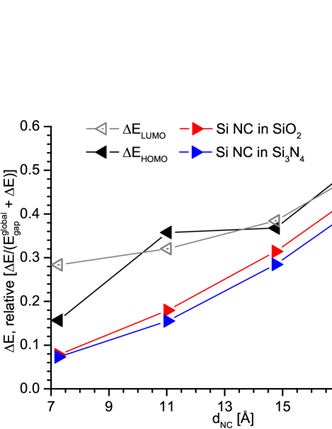
The total NC ionization in Fig. 6 only shows minor deviations from the ionization of -octahedral N Cs with OH/NH2-termination, see Fig. 3, confirming that both 18.5 Å Si-NCs (Si165) are still within range of ICT saturation. These minor deviations are instructive to understand the impact of O vs. N onto dns-Si, see Sec. V.
For all NC sizes, N-terminated Si-NCs slightly increase their ionization from coverage with all-around 1.5 ML Si3N4 via inclusion into 1 to 3 ML Si3N4 in Sin approximants up to all-around 1ML Si3N4 coverage. As pointed out in Sec. III.1, this increase with decreasing thickness of Si3N4-embedding originates from the positive electron affinity of N. The 1 to 3 ML Si3N4 coverage takes an intermediate position between full coverages with 1 and 1.5 ML Si3N4. In other words, the 1 ML Si3N4 coverage of the outer NC interface in Sin approximants does not delocate and/or deflect valence electron wavefunctions originating from Si-NC atoms enough to provide a full upshift of energy levels. Arguably, and backed by experimental data (Sec. IV), the electronic states of Si3N4-embedded NCs in the Sin approximants could be located nearer if a complete multi-ML embedding in Si3N4 with heavy atoms could be computed.
For Si-NCs in SiO2, NC ionization increases from 1 ML via 1.5 ML SiO2 to embedding in 1 to 3ML SiO2 in Sin approximants. Here, the strong localization of valence electrons from Si-NCs at O drives the ionization process and thus the shift of valence electron wavefunctions of the Si-NC to higher binding energies. We thus can presume an average 2 ML embedding in SiO2 for the Sin approximants, yielding 1, 1.5 and 2 ML for the increasing ionization of Si-NCs by SiO2, clearly correlating with the number of O atoms per Si-NC atom.
To recapitalize, also exists in the complete system manifested by Sin approximants, one embedded each in SiO2 and Si3N4. The strength of increases with NC separation given by the combined inter-NC thickness of SiO2 and Si3N4, though not quite reaching the values for individual NCs in SiO2 vs. Si3N4. As a likely cause we identified the transition range between SiO2 and Si3N4 where the nature of both anions – O and N – tend to cancel each others impact on the electronic structure. Apart from proving the full scale of in a complete system, the Sin approximants investigated in this section yield to a more detailed evaluations of NC ionization and .
IV Experimental Results: Synchrotron UPS
After an initial UPS measurements confirming the effect of for Si-NWells in SiO2 vs. Si3N4 König et al. (2018b), we characterized 10 SiO2- and 4 Si3N4-embedded NWells with thicknesses ranging from 11 to 50 Å. Since we work with NWells and thus quasi-2D band structures, we replace and with the energy of the highest occupied viz. top valence band states and of the lowest unoccupied states viz. bottom conduction band , respectively, to account for the limits on continuous electronic DOS. Details on deriving the ionization energy of such valence band states and respective standard deviations are treated in Appendix Sec. A and in König et al. (2018c). Fig. 7 shows values as a function of NWell thickness for SiO2- and Si3N4-embedding.
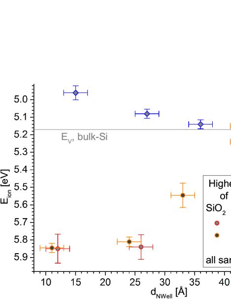
For to 15 Å, we obtained eV for NWells in SiO2 and eV for NWells in Si3N4. For SiO2-embedding, a minute change to eV occurs for Å. Changes are more notable for Si3N4-embedding where we obtained eV for Å. We also note that changes rather continuously as compared to NWells embedded in SiO2 which is subject to discussion in Sec. V. In the range of to 40 Å, of Si-NWells in SiO2 and Si3N4 change to approach the common value eV as known for bulk-Si. Expressing these values in terms of , we get eV and eV, decreasing to eV and eV. The difference in for Si-NWells embedded in SiO2 vs. Si3N4 thus undergoes a minor decrease from 0.89 eV for Å to 0.74 eV for Å. Since Si-NWells have significantly lower fundamental gaps as compared to Si-NCs (cf. Figs. 4 and 5), a pronounced n/p-type charge carrier preference arises from the energy offsets above for Å.
We are planning to measure the conduction band states of NWell samples along with UPS characterizations on the same samples, motivated by Zimina et al. Zimina et al. (2006) who characterized of Si-NCs embedded in SiO2 for to 40 Å by soft X-ray emission spectroscopy (SXES). A downshift of up to 0.2 eV below the conduction band edge of bulk-Si was obtained Zimina et al. (2006). Conventional quantum physics strongly suggests to be located a few 100 meV above of bulk-Si which already includes contributions from excitonic binding and dielectric screening. The same work also noted that the interface of Si-NCs is not abrupt but rather gradual, with sub-oxide shells in a thickness range of 3 to 5 Å. This value is likely underestimated since similar superlattices of Si-NCs with sub-oxide shells characterized by atom probe tomography were found to have sub-oxide shells of ca. 8 Å Gnaser et al. (2014); König et al. (2015). Such thicker sub-oxide shells will attenuate the ICT and thus due to the sub-oxide not having the full impact onto dns-Si and working as an electrostatic buffer between the Si-NC and SiO2 at the same time. Since our NWell samples have plane interfaces and were not processed by excess Si segregation from a sub-oxide Heitmann et al. (2005), the interface thickness is on the order of 5 Å as occurring in conventional c-Si oxidation Afanas’ev et al. (2001). Hence, it appears that higher energy offsets and consequently exist for NWells as compared to Si-NCs formed by segregation from Si-rich dielectrics Heitmann et al. (2005); Hiller et al. (2014).
To sum up, for NWells with to 50 Å in both, SiO2 and Si3N4. We take this value as the common baseline from which to count with decreasing as per dielectric. For to 40 Å, a transition range exists with increasing between NWells in SiO2 vs. Si3N4. At Å, the respective are fully developed with eV, still increasing to eV for to 15 Å. Thus, a strong n/p-type carrier preference exists for dns-Si in SiO2/Si3N4 which can induce a p/n junction for Å, cf. Fig. 5g-i. Published characterisation data on Si-NCs prepared by segregation anneal from Si-rich SiO2 Zimina et al. (2006) show negative , resulting in eV. As electronic quality and abruptness of the interface of Si-NWells is notably superior to segregated Si-NCs having warped/multi-faceted interfaces, the negative of NWells should be more pronounced in SXES measurements.
V Proposed Mechanism of Energy Offset
With the quantitative theoretical and experimental data presented above, we propose a qualitative model for the energy offsets and induced by embedding in SiO2 vs. Si3N4. From there, we determine the impact length of and in dns-Si systems.
V.1 Basic Principle
A brief look at some element-specific quantum-chemical parameters of O, N and Si as listed in Table 2 is very helpful to explain .
| 222refers to first valence electron | EN333values after Allred & Rochow | IOB | to Si | |||
|---|---|---|---|---|---|---|
| [eV] | [eV] | [%] | [Å] | |||
| N | 14.53 | 0.07 | 3.07 | 36 | 0.1743 | (Si3N4) |
| O | 13.36 | 1.46 | 3.50 | 54 | 0.1626 | (SiO2) |
| Si | 8.15 | 2.08 | 1.74 | 0 | 0.2387 | (bulk Si)444 with unit cell length of 0.5431 nm CoD (2014) |
For O, the explanation of is fairly straightforward. With a high negative and an ionicity of bond (IOB) to Si of ca. 53 %, O localizes electronic charge from dns-Si, thereby increasing the binding energy of such electrons which present the valence states of dns-Si with the lowest binding energy. As a consequence, (dns-Si) is shifted further below . Since Si atoms have a reasonably high which counteracts electron removal, the ICT feeding into electron localization at O decreases from its saturation value (maximum positive ionization) after a few MLs of the dns-Si system. Eventually, the impact of the ICT due to O at the dns-Si interface vanishes, whereby . The top graph of Fig. 8 illustrates this behavior.
The situation with N requires some broader considerations of its properties. Out of all chemical elements which are known to expose anionic properties (main groups IV to VII of the periodic table), N is the only element which possesses a positive electron affinity , meaning that turning N into a negative ion (a Lewis acid Holleman et al. (1995)) requires a significant activation energy. Therefore, N is very reluctant to accept negative charge as from dns-Si, which becomes even more prominent when compared to O. This fact is well known from some basic chemical reactions such as creating ammonia (NH3) from the elements,
requiring a catalytic iron contact at 300 bar and 650 ∘C to trigger above reaction known as Haber-Bosch synthesis Holleman et al. (1995). In contrast, O reacts violently with H at room temperature at 1 bar (oxyhydrogen reaction) Holleman et al. (1995):
Considering Si, oxidation of Si surfaces to SiO2 in elemental O2 proceeds readily at room temperature and is promoted by the presence of H2O. In contrast, the nitridation reaction requires Si surfaces to be offered atomic/ionic N in a plasma several 100 ∘C above room temperature to achieve the reaction.
This uncommon behavior of N is at the heart of the energy offset: While N delocalizes electrons of a dns-Si system at the top of its valence band, it does not localize such electrons, but rather deflects them back into the dns-Si and adjacent Si3N4. This delocalization results in a lower binding energy of these valence electrons. From Fig. 7 we also see that the delocalizing impact of N onto does not show a strict saturation for Å as is the case for SiO2-embedding. This behavior has to be seen in the context of electron delocalization which is more sensitive to environmental changes such as an increase of the number of NWell Si atoms per N atom in Si3N4. We can therefore state that generated by Si3N4-embedding is not as robust as due to SiO2.
The partial deflection of delocalized electrons into the first couple of ML of Si3N4 explains the stronger shift of and towards for -octahedral Si-NCs in 1.5 ML vs. 1 ML Si3N4, cf. Fig. 4. The same consequence occurs when going from -octahedral to -cubic Si-NCs, where the ratio increases significantly. To add, such behavior can clearly be seen for the frontier OMOs at approximants featuring a Si-NC in Si3N4 plus a Si-NC in SiO2, see Sec. III.2 and Fig. 5b, e and h. The resulting shift of towards within the first few MLs of dns-Si is shown in the bottom graph of Fig. 8.
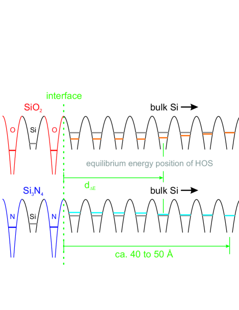
Fig. 7 shows that . This finding correlates qualitatively with the IOB of N vs. O to Si. Other factors as anion-to-Si ratio, positive (N) vs. negative (O), bond length and packing fraction in the dielectric have an influence on this ratio as well.
Since we intent to use the for undoped p/n junctions, we consider it useful to define its impact length as the distance from the dns-Si interface to the point where comes out of saturation. This definition of provides the optimum impact for undoped p/n-junctions since the global energy gap of the dns-Si system decreases with its increasing size, see Fig. 9.
V.2 Calculation of Impact Length of in dns-Si
From the measurements of by synchrotron UPS, we derived Å as the saturation limit beyond which decreases significantly. NWells have two adjacent interfaces which immediatley yields Å. This value presents the limit for the semi-infinite case, id est an interface to bulk-Si. The volume element defining is a cubicle of height , its width and length is defined by the smallest periodic unit in the respective direction. For NWells, we thus get , arriving at the value obtained by synchrotron UPS, see right graph in Fig 10.
As an approximation, NWires and NCs have warped interfaces which do not allow for a straightforward derivation of as is the case for NWells and bulk-Si. Therefore, we derive the gauge for these dns-Si systems by simple geometric arguments of volume integration via Riemann’s sums Zeidler et al. (2004). For NWires, we cut out a slab which presents the smallest periodic unit along the NWire axis. This slab is then filled with volume elements , presenting the Riemann sum of the slab volume. For NWires, these are wedges, see center graph in Fig. 10. With , we achieve the transition from the Riemann sum to the volume integral, resulting in an infinite number of wedges with vanishing base area. With equal base areas, the volume of a wedge equals the volume of a cubicle if the height of the wedge is twice the height of the cubicle. Consequently, the impact length of doubles when going from NWells to NWires, resulting in . For NCs, it is straightforward that we get pyramids as volume elements , see left graph in Fig. 10. With the same base area, a pyramid has the same volume as a cubicle if its height is three times the height of the cubicle. Accordingly, we obtain . Summarizing all definitions, we get scaling with bulk-Si : NWell : NWire : NC like 1 : 2 : 4 : 6. With Å, we get Å and Å.
In real systems, the rise in with decreasing dimensionality of the dns-Si system should be sublinear, originating from a higher defect density due to warped interfaces which has to be controlled by as well. We can account for this effect by exploiting the fact that fundamental gaps of Si-NCs are significantly bigger for Si3N4-embedding vs. SiO2-embedding if such NCs are small enough König et al. (2008, 2014). Experimental data showed of both embeddings to converge at Å Ehrhardt et al. (2013). Assuming a reduction factor per reduced dimension and using , we arrive at , yielding Å and Å below which is saturated.
VI Conclusions
We presented a detailed quantitative study of considerable energy offsets of frontier electronic states as a new fundamental effect arising from deep nanoscale (dns-) Si volumes when embedded/coated in SiO2 vs. Si3N4.
Using DFT, we investigated single Si-NCs as a function of interface orientation and thickness of embedding SiO2 vs. Si3N4 up to Å. We found and to have little dependence on NC size in the range considered, showing a strong offset due to 1.5 ML SiO2- vs. Si3N4-embedding of eV and eV. These offsets push and of SiO2-embedded Si-NCs further below , while shifting and of Si3N4-embedded Si-NCs towards . Extending the embedding in SiO2/Si3N4 beyond 1 ML and in particular increasing the ratio of interface bonds per NC atom by going from -octahedral to -cubic NCs increased further. As ultimate theoretical test, we computed approximants featuring two Si-NCs of up to 18.5 Å size, one each embedded in SiO2 and Si3N4, respectively, confirming within one system.
We characterized 14 samples, each featuring one Si-NWell of to 50 Å embedded in SiO2 or in Si3N4, by long-term synchrotron UPS to measure the energy of the top valence band states . For Å, we obtained to 0.74 eV for SiO2- vs. Si3N4-embedding. After a transition range at to 40 Å, Si-NWells in both embeddings converge to . Zimina et al. Zimina et al. (2006) found the energy of the lowest unoccupied states at eV for SiO2-embedded Si-NCs, whereby attractive interactions like exciton binding energy and screening were already included in this value. This finding is consistent with our results on of thin Si-NWells in SiO2.
Investigating the quantum chemistry of O and N with respect to Si, we proposed a model for . The uncommon situation of N as the only anionic element with an electron affinity eV and a yet fairly high electronegativity EN inducing a strong polar bond to Si is one cornerstone of the newly discovered effect. While N delocalizes valence electrons from dns-Si, it does not localize such electrons but deflects these back into dns-Si or surrounding Si3N4 as also evident from frontier OMO density plots in DFT calculations spreading well into Si3N4. As a consequence, such delocalized NWell valence band states have a lower binding energy which is equivalent to an upshift of towards . As expected, the strong conventional anionic nature of O results in strong localization of valence electrons from dns-Si at O in SiO2 and an associated downshift of below .
With a straightforward geometrical Riemann model, we calculated the impact length up to which governs the electronic structure of dns-Si to scale 1 : 2 : 4 : 6 for bulk-Si : NWell : NWire : NC. With Å, we thus arrived at Å and Å. The latter two dns-Si structures have warped interfaces which are more prone to defects; experimental data from the literature on the difference on the fundamental gap of Si-NCs embedded in SiO2 vs. Si3N4 yielded Å. We introduced a dimensionality factor per reduced dimension (NWells NWires NCs) of , accounting for an increased number of defects at warped interfaces, yielding Å and matching Å.
The in dns-Si by coating with or embedding in SiO2 (Si3N4) induces a strong preference for electrons (holes) and thus to n(p)-type Si. Application to dns-Si would eliminate all issues of impurity doping – out-diffusion, clustering, self-purification, ionization at room and cryogenic temperatures, inelastic carrier scattering – and extend device miniaturization potentially down to the minimum size of Si crystallites of ca. 1.5 nm Schuppler et al. (1994) along with much reduced bias voltages and heat loss.
Acknowledgements.
D. K. wishes to thank J. Rudd for compute cluster administration and acknowledges use of the Abacus compute cluster, IMDC, UNSW, funding by the 2015 UNSW Blue Sky Research Grant and by the 2018 Theodore-von-Kàrmàn Fellowship of RWTH Aachen University, Germany. D. K. and D. H. acknowledge funding by 2012, 2014 and 2016 DAAD-Go8 joint research cooperation schemes. D. H. acknowledges the Alexander von Humboldt Foundation for a Feodor Lynen Fellowship and the German Research Foundation (DFG) for funding (HI 1779/3-1). The authors thank L. Sancin at Elettra Synchrotron for technical support. N. W., B. B. and J. K. acknowledge support by the Impulse and Networking Fund of the Helmholtz Association.Appendix A Evaluation of UPS Data
In our recent publication, we discussed the calibration of UPS-Scans and data extraction by local fitting of amorphous backgrounds using Si3N4-embedded Si-NWells of 17 and 27 Å thickness in much detail König et al. (2018c).
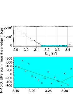
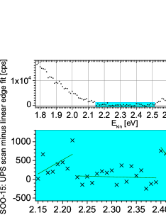
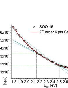
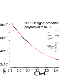
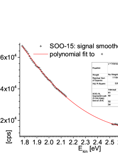
Here, we just focus on one SiO2- and one Si3N4-embedded sample for determining the valence band edge, its standard deviation over energy and associated local background fitting per scan to explain the principle. We further explain several plausibility tests as an additional means to arrive at the correct data. As examples, we pick UPS scans of sample N-15-D, comprising a 15 Å Si-NWell in Si3N4, and of sample SOO-15, comprising a 12 Å Si-NWell in SiO2. Both scans have the lowest signal-to-noise ratio (SNR) against the background due to secondary electrons and SiO2/Si3N4. This circumstance predestines both samples to demonstrate the UPS data filtering algorithm to obtain the valence band edge of buried Si-NWells. Fig. 11 shows the global UPS scans of both samples which were measured during beamtime 1 at the BaDElPh beamline at the Elettra Sincrotrone Trieste, Italy, cf. Fig. 7. Common parameters are the UV photon energy of eV and the background cps value of 1950 which was derived in the interval of eV = [8.7;8.2] eV. This background cps value derived from the Si reference serves as calibration standard and thus sets the cps intercept for all UPS scans, see König et al. (2018c) for details.

(a) (b)
Below, we describe the algorithm to determine the valence band edge of a Si-NWell embedded in Si3N4 or SiO2.
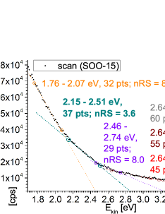
We begin by checking the UPS scan for regions of reasonably linear values with points, equivalent to an range of 0.15 eV. The following steps are applied to every linear region found. We assign the number of points forming the linear region to . We then run a linear fit over the edge region, calculate its sum of residual squares (RS) and its average cps value . With these three values, we can calculate the normalized RS (nRS) which takes into account the signal intensity and length of the linear region: . The linear region with the minimum nRS is the edge of the Si-NWell, subject to passing a number of plausibility tests lined out below. The intercept of the linear fit provides the value which yields to the valence band top of the Si-NWell via . Fig. 12 shows the range of interest per UPS scan with all linear regions detected.
(a) (b)
(a) (b)
(a) (b)
Next, we calculate the standard deviation , using the difference between the UPS signal and its linear fit, cf. Fig. 13. Within the edge region, we group points with associated alignment. For these, we calculate local fits and determine their intercepts, cf. Fig. 14. The resulting values are used together with the value of the linear fit to the entire edge region to determine Zeidler et al. (2004) and are shown as error bars of in Fig. 7. We note that – as samples were measured at K – the minimum error bar for is set to eV.
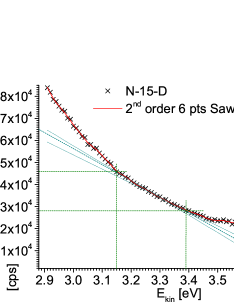
Since the algorithm on its own may yield a couple of possible solutions, we carry out additional plausibility tests. One of them is a combination of the smoothed UPS signal, an associated background fit and the interpolation of the resulting differential signal. First, we take the UPS data of the edge region plus one energy range as defined by the edge region above and below the edge (e.g. N-15-D has an edge from to 3.39 eV [25 pts], we now pick UPS data from 2.90 to 3.64 eV [ pts]). To this data set, we apply a Sawitzky-Golay smoothing Savitzky and Golay (1964) over 6 points with a order polynomial as an effective means to remove single point runaways without altering the spectral information, cf. Fig. 14. Thereby, we get less noisy UPS data in the range of interest. This smoothed UPS data is used for a background fit, whereby we exclude the actual edge region ( to 3.39 eV [25 pts] for sample N-15-D). Since higher order polynomials can be interpreted as the finite Taylor series of an exponential function, , we choose polynomials to fit the background and use the signal calibration intercept of 1950 cps as the coefficient for , see Fig. 15. While the coefficients of the decrease from , qualitatively agreeing with the Taylor series of an exponential function, there is still some degree of freedom to adapt to local deviations. These are evident even after Sawitzky-Golay smoothing, cf. Figs. 12 and 15. An exponential behavior of the signal background originates from the Urbach tails of the amorphous dielectric Böer (1990), with additional contributions due to inelastic electron scattering.
(a) (b)
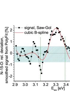
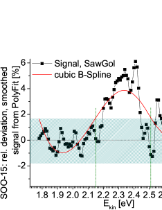
We now can calculate the difference between the smoothed UPS signal and the background fit where the edge region shows up above the noise, cf. Fig. 16. Due to the finite error in background fitting, there are local deviations of the fit from data points in the local environment of the edge region which cannot be accounted for. As a consequence, the first few points outside the edge region tend to be further away from the background fit which can cause a dumping of the first few data points within the edge region. We also note that the fit does not account for an irregular, rather rapid low amplitude oscillation of the UPS signal. Hence, we have to look for positive signals – the edge signal occurs on top of the background – on a prolonged energy scale, ruling out rapid oscillations. To this end, we run a cubic B-Spline interpolation Zeidler et al. (2004) on the differential signal which minimizes the oscillatory behavior, cf. Fig. 16.
(a) (b)
Another plausibility test is given by measuring NWell samples of different with a dielectric top layer of possibly constant thickness. Assuming that the dielectric top layer and its interface to the NWell have exactly the same thickness for all samples per dielectric type and all measurement conditions are constant, the signal intensity (cps) of the NWell is related to the layer thickness of the top dielectric layer and via , reducing to for . The average inelastic mean free path of excited electrons is presented by . For brevity, we introduce one value for Si-NWell and the respective dielectric. It is interesting to note that has been overestimated in UPS for several compounds Offi et al. (2008); Iacobucci et al. (2019) since its widely used empirical description by Seah and Dench Seah and Dench (1979) was derived for many chemical elements and compounds for eV but only for three compound materials using eV. In a perfect world, we should see a cps increasing asymptotically with . In reality, minor thickness deviations in particular of the top dielectric layer will soften this asymptotic behavior into a cps monotonically increasing with , cf. Fig. 17.
As for UPS signal quality, we can state that the SNR is higher for Si-NWells embedded in SiO2 vs. Si3N4. This finding may come as a surprise as the average cps per edge region is higher for NWells embedded in Si3N4 vs. SiO2. However, the difference in valence band top energies is to 1.88 eV Keister et al. (1999); König et al. (2018c) and to 4.54 eV Keister et al. (1999); König et al. (2018c). As a consequence, the Urbach tails of the amorphous Si3N4 layers deliver a significantly higher contribution to the UPS signal as opposed to SiO2, cf. Fig. 11. To add, the packing fraction of Si3N4 and the density of electronic defects is notably higher as compared to SiO2. This finding is also reflected in the bigger range of the valence band offset from Si3N4 to bulk-Si of ca. 0.1 eV as opposed to the value from SiO2 to bulk-Si (0.01 eV).


(a) (b)
References
- Pearson and Bardeen (1949) G. L. Pearson and J. Bardeen, Phys. Rev. 17, 865 (1949).
- Koelling et al. (2013) S. Koelling, O. Richard, H. Bender, M. Uematsu, A. Schulze, G. Zschaetzsch, M. Gilbert, and W. Vandervorst, Nano Letters 13, 2458 (2013).
- Kambham et al. (2013) A. K. Kambham, A. Kumar, A. Florakis, and W. Vandervorst, Nanotechnology 24, 275705 (2013).
- Duffy et al. (2018) R. Duffy, A. Ricchio, R. Murphy, G. Maxwell, R. Murphy, G. Piaszenski, N. Petkov, A. Hydes, D. O’Connell, C. Lyons, N. Kennedy, B. Sheehan, M. Schmidt, F. Crupi, J. D. Holmes, P. K. Hurley, J. Connolly, C. Hatem, and B. Long, J. Appl. Phys. 123, 125701 (2018).
- Heitmann et al. (2005) J. Heitmann, F. Müller, M. Zacharias, and U. Gösele, Adv. Mater. 17, 795 (2005).
- Dalpian and Chelikowsky (2006) G. M. Dalpian and J. R. Chelikowsky, Phys. Rev. Lett. 96, 226802 (2006).
- Stegner et al. (2009) A. R. Stegner, R. N. Pereira, R. Lechner, K. Klein, H. Wiggers, M. Stutzmann, and M. S. Brandt, Phys. Rev. B 80, 165326 (2009).
- Chan et al. (2008) T.-L. Chan, M. L. Tiago, E. Kaxiras, and J. R. Chelikowsky, Nano Lett. 8, 596 (2008).
- König et al. (2015) D. König, S. Gutsch, H. Gnaser, M. Wahl, M. Kopnarski, J. Göttlicher, R. Steininger, M. Zacharias, and D. Hiller, Sci. Rep. 5, 09702 (2015).
- Pereira et al. (2012) R. N. Pereira, A. J. Almeida, A. R. Stegner, M. S. Brandt, and H. Wiggers, Phys. Rev. Lett. 108, 126806 (2012).
- Hiller et al. (2017) D. Hiller, J. López-Vidrier, S. Gutsch, M. Zacharias, M. Wahl, W. Bock, A. Brodyanski, M. Kopnarski, K. Nomoto, J. Valenta, and D. König, Sci. Rep. 7, 8337 (2017).
- Hiller et al. (2018a) D. Hiller, J. López-Vidrier, K. Nomoto, M. Wahl, W. Bock, T. Chlouba, F. Trojànek, S. Gutsch, M. Zacharias, D. König, P. Malý, and M. Kopnarski, Beilstein J. Nanotech. 9, 1501 (2018a).
- Dingle et al. (1978) R. Dingle, H. L. Störmer, A. C. Gossard, and W. Wiegmann, Appl. Phys. Lett. 33, 665 (1978).
- König et al. (2017) D. König, D. Hiller, S. Gutsch, M. Zacharias, and S. Smith, Sci. Rep. 7, 46703 (2017).
- Hiller et al. (2018b) D. Hiller, J. Göttlicher, R. Steininger, T. Huthwelker, J. Julin, F. Munnik, M. Wahl, W. Bock, B. Schoenaers, A. Stesmans, and D. König, ACS Appl. Mat. Interfaces 10, 30495 (2018b).
- König et al. (2018a) D. König, D. Hiller, and S. Smith, Phys. Rev. Appl. 10, 054034 (2018a).
- König and Rudd (2013) D. König and J. Rudd, AIP Adv. 3, 012109 (2013).
- Liu et al. (2018) C.-C. Liu, E. Franke, Y. Mignot, R. Xie, C. W. Yeung, J. Zhang, C. Chi, C. Zhang, R. Farrell, K. Lai, H. Tsai, N. Felix, and D. Corliss, Nat. Electron. 1, 562 (2018).
- Schuppler et al. (1994) S. Schuppler, S. L. Friedman, M. A. Marcus, D. L. Adler, Y. H. Xie, F. M. Ross, T. D. Harris, W. L. Brown, Y. J. Chabal, L. E. Brus, and P. H. Citrin, Phys. Rev. Lett. 72, 2648 (1994).
- König et al. (2018b) D. König, D. Hiller, N. Wilck, B. Berghoff, M. Müller, S. Thakur, G. D. Santo, L. Petaccia, J. Mayer, S. Smith, and J. Knoch, Beilstein J. Nanotech. 9, 2255 (2018b).
- Berglund and Spicer (1964) C. N. Berglund and W. E. Spicer, Phys. Rev. 136, A1030 (1964).
- Berglund and Spicer (1999) C. N. Berglund and W. E. Spicer, Phys. Rev. 136, A1044 (1999).
- Reinert and Hüfner (2005) F. Reinert and S. Hüfner, New J. Phys. 7, 97 (2005).
- Suga and Sekiyama (2014) S. Suga and A. Sekiyama, Photoelectron Spectroscopy, Springer Series in Optical Sciences, Vol. 176 (Springer, Berlin, 2014).
- König et al. (2018c) D. König, D. Hiller, N. Wilck, B. Berghoff, M. Müller, S. Thakur, G. D. Santo, L. Petaccia, J. Mayer, S. Smith, and J. Knoch, Beilstein J. Nanotech. 9, 2255 (2018c), supporting information; https://www.beilstein-journals.org/bjnano/content/supplementary/2190-4286-9-210-S1.pdf ; accessed .
- G09 (2010) Gaussian09, Revision D.01, M. J. Frisch, et. al., Gaussian, Inc., Wallingford, CT (2010).
- Gordon et al. (1982) M. S. Gordon, J. S. Binkley, J. A. Pople, W. J. Pietro, and W. J. Hehre, J. Am. Chem. Soc. 104, 2797 (1982).
- Becke (1988) A. D. Becke, Phys. Rev. A 38, 3098 (1988).
- Lee et al. (1988) C. Lee, W. Yang, and R. G. Parr, Phys. Rev. B 37, 785 (1988).
- Francl et al. (1982) M. M. Francl, W. J. Pietro, W. J. Hehre, J. S. Binkley, D. J. DeFrees, J. A. Pople, and M. S. Gordon, J. Chem. Phys. 77, 3654 (1982).
- König et al. (2008) D. König, J. Rudd, M. A. Green, and G. Conibeer, Phys. Rev. B 78, 035339 (2008).
- König et al. (2014) D. König, D. Hiller, S. Gutsch, and M. Zacharias, Adv. Mater. Interfaces 1, 1400359 (2014).
- Rissner et al. (2011) F. Rissner, D. A. Egger, A. Natan, T. Körzdörfer, S. Kümmel, L. Kronik, and E. Zojer, J. Am. Chem. Soc. 133, 18634 (2011).
- Dennington et al. (2009) R. Dennington, T. Keith, and J. Millam, “GaussView 5.0.8,” (2009).
- Hiller et al. (2014) D. Hiller, A. Zelenina, S. Gutsch, S. A. Dyakov, L. Lòpez-Conesa, J. Lòpez-Vidrier, S. Estradé, F. Peiró, B. Garrido, J. Valenta, M. Koínek, F. Trojánek, P. Malý, M. Schnabel, C. Weiss, S. Janz, and M. Zacharias, J. Appl. Phys. 115, 204301 (2014).
- Petaccia et al. (2009) L. Petaccia, P. Vilmercati, S. Goronikov, M. Barnaba, A. Bianco, D. Cocco, C. Masciovecchio, and A. Goldoni, Nucl. Instr. Meth. in Phys. Res. A 606, 780 (2009).
- Thust et al. (2016) A. Thust, J. Barthel, and K. Tillmann, Journal of large-scale research facilities JLSRF 2, A41 (2016), DOI: 10.17815/jlsrf-2-66.
- König (2016) D. König, AIP Adv. 6, 085306 (2016).
- König and Smith (2019) D. König and S. C. Smith, Acta Cryst. B (2019), in review, see https://arxiv.org/pdf/1901.00935.pdf for draft.
- Hesketh et al. (1993) P. J. Hesketh, C. Ju, S. Gowda, E. Zanoria, and S. Danyluk, J. Electrochem. Soc. 140, 1080 (1993).
- Holleman et al. (1995) A. F. Holleman, E. Wiberg, and N. Wiberg, Lehrbuch der Anorganischen Chemie (101. Ed.) (Walter deGruyter, Berlin, 1995) in German.
- Guerra et al. (2009) R. Guerra, E. Degoli, and S. Ossicini, Phys. Rev. B 80, 155332 (2009).
- Note (1) There are 2 ML, 3 ML, 4 ML and 4.5 ML of SiO2 plus Si3N4 for the Si10-, Si35-, Si84- and Si165-approximants separating the NCs. Increasing inter-NC layer thickness of the combined dielectrics or thickness of the dielectric at outer NC facets is not possible at present due to intractability of DFT computations for heavy atoms with the level of theory we use.
- Zimina et al. (2006) A. Zimina, S. Eisebitt, W. Eberhardt, J. Heitmann, and M. Zacharias, App. Phys. Lett. 88, 163103 (2006).
- Gnaser et al. (2014) H. Gnaser, S. Gutsch, M. Wahl, R. Schiller, M. Kopnarski, D. Hiller, and M. Zacharias, J. Appl. Phys. 115, 034304 (2014).
- Afanas’ev et al. (2001) V. V. Afanas’ev, M. Houssa, A. Stesmans, and M. M. Heyns, Appl. Phys. Lett. 78, 3073 (2001).
- CoD (2014) “The NIST Reference on Constants, Units and Uncertainties – Fundamental Physical Constants (2014 edition),” (2014), https://physics.nist.gov/cgi-bin/cuu/Value?asil ; accessed .
- Zeidler et al. (2004) E. Zeidler, W. Hackbusch, and H. R. Schwarz, Oxford User’s Guide to Mathematics (Oxford University Press Inc., New York, 2004) translated from German by Bruce Hunt.
- Ehrhardt et al. (2013) F. Ehrhardt, G. Ferblantier, D. Muller, C. Ulhaq-Bouillet, H. Rinnert, and A. Slaoui, J. Appl. Phys. 113, 033528 (2013).
- Savitzky and Golay (1964) A. Savitzky and M. J. E. Golay, Anal. Chem. 36, 1627 (1964).
- Böer (1990) K. W. Böer, Survey of Semiconductor Physics, Vol. 1 (Van Nostrand Reinhold, New York, 1990).
- Offi et al. (2008) F. Offi, S. Iacobucci, P. Vilmercati, A. Rizzo, A. Goldoni, M. Sacchi, and G. Panaccione, Phys. Rev. B 77, 201101(R) (2008).
- Iacobucci et al. (2019) S. Iacobucci, F. Offi, P. Torelli, and L. Petaccia, J. Electron Spectr. Related Phenomena 233, 1 (2019).
- Seah and Dench (1979) M. P. Seah and W. A. Dench, Surf. Interface Anal. 1, 2 (1979).
- Keister et al. (1999) J. W. Keister, J. E. Rowe, J. J. Kolodziej, H. Niimi, T. E. Madey, and G. Lucovsky, J. Vac. Sci. Tech. B 17, 1831 (1999).