Electronic structure of Bi2Te3/FeTe heterostructure: implications for unconventional superconductivity
Abstract
We have performed angle-resolved photoemission spectroscopy on a heterostructure consisting of topological insulator Bi2Te3 and iron chalcogenide FeTe fabricated on SrTiO3 substrate by molecular-beam-epitaxy technique. This system was recently found to show superconductivity albeit non-superconducting nature of each constituent material. Upon interfacing FeTe with two quintuple layers of Bi2Te3, we found that the Dirac-cone surface state of Bi2Te3 is shifted toward higher binding energy, while the holelike band at the Fermi level originating from FeTe moves toward lower binding energy. This suggests that electron charge transfer takes place from FeTe to Bi2Te3 through the interface. The present result points to importance of hole-doped FeTe interface for the occurrence of unconventional superconductivity.
pacs:
71.20.-b, 74.78.-w, 79.60.-iSuperconductivity associated with an interface of two parent materials is recently attracting tremendous attention because it often becomes a platform of unconventional superconductivity owing to the peculiar characteristic of interface that has circumstances different from bulk. One such example is a charge accumulation at the interface and the resultant emergence of metallicity and superconductivity, as highlighted by the observation of superconductivity at the interface of insulating LaAlO3 (LAO) and SrTiO3 (STO) LAOSTO1 ; LAOSTO2 . The interface also plays a crucial role in controlling the superconducting transition temperature, , as recognized from a significant enhancement of in FeSe on STO (over 65 K) compared to that in bulk FeSe (8 K), associated with a charge transfer across the interface and an interfacial electron-phonon coupling FeSeSTO1 ; FeSeSTO2 ; FeSeSTO3 . Also, a widely used strategy to realize topological superconductivity relies on interfacing conventional superconductors and nano-wires/ultrathin films to utilize superconducting proximity effect though the interface. Thus, it is important to find a new platform of interfacial superconductivity and establish the role of interface to unusual superconducting properties.
Recently, it has been reported that a heterostructure consisting of topological insulator Bi2Te3 and a parent compound of iron-chalcogenide superconductors FeTe hosts interfacial superconductivity BiTeFeTe1 . Whereas both Bi2Te3 and FeTe are non-superconducting, superconductivity appears around 2 K after interfacing one quintuple layer (QL) of Bi2Te3 with a thick FeTe film. The increases with increasing the number of Bi2Te3 QLs, and reaches the highest value of 12 K at 5 QL BiTeFeTe1 , which is about ten times higher than that of a prototypical interfacial superconductor LAO/STO LAOSTO2 . Also, two-dimensional (2D) character of superconductivity was verified by observations of a Berezinsky-Kosterlitz-Thouless transition and the temperature dependence of upper critical field that follows the Ginzburg-Landau theory for 2D superconductor films BiTeFeTe1 . These findings triggered intensive investigations on Bi2Te3/FeTe heterostructure BiTeFeTe2 ; BiTeFeTe3 ; BiTeFeTe4 ; BiTeFeTe5 ; BiTeFeTe6 ; BiTeFeTe7 and, consequently, several peculiar properties such as coexistence of multiple gaps in the superconducting state BiTeFeTe6 and enhancement of up to 20 K under hydrostatic pressure BiTeFeTe7 have been reported. However, the origin of interfacial superconductivity in Bi2Te3/FeTe is still under debate partly because of the lack of detailed understanding of the electronic states. Besides basic interests in the interfacial superconductivity, Bi2Te3/FeTe is also attracting attention as a new topological-superconductor candidate. If the topological Dirac-cone band of Bi2Te3 is preserved at the surface or interface, the heterostructure of Bi2Te3/FeTe would provide a rare opportunity to search for Majorana fermions at relatively high temperatures. To clarify the origin of interfacial superconductivity and the possibility of topological superconductivity, the experimental determination of the electronic states in Bi2Te3/FeTe is of crucial importance.
In this paper, we report angle-resolved photoemission spectroscopy (ARPES) study on Bi2Te3/FeTe heterostructure grown by molecular-beam epitaxy (MBE). We directly observed the evolution of the electronic states upon interfacing Bi2Te3 with FeTe. We found the occurrence of a charge transfer through the interface and the presence of a topological Dirac-cone band derived from Bi2Te3. We discuss the implications of the present results for the origin of interfacial superconductivity and the topological property in Bi2Te3/FeTe.
Heterostructures of Bi2Te3 and FeTe films were fabricated on a Nb (0.05 wt)-doped STO substrate with the MBE method. The substrate was first degassed at 600 ∘C for 5 h and then heated at 900 ∘C for 30 min. Next, a 10-monolayer (ML) FeTe film was grown by co-evaporating Fe and Te in a Te-rich condition while keeping the substrate temperature at 270 ∘C. Finally, we fabricated -QL Bi2Te3 film ( = 2 and 6) on the FeTe film by co-evaporating Bi and Te at the substrate temperature of 270 ∘C. We also fabricated a 6-QL Bi2Te3 film on Si(111) as a reference. After the growth, films were annealed under ultrahigh vacuum and characterized by - ARPES measurements. ARPES measurements were performed using Scienta-Omicron SES2002 and MBS-A1 spectrometers with He and Xe discharge lamps ( = 21.218 and 8.437 eV, respectively) at Tohoku University. The energy and angular resolutions were set to be 7-30 meV and 0.2∘, respectively.
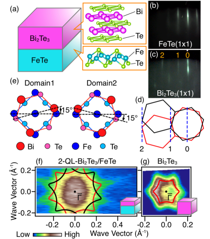
First, we present characterization of Bi2Te3/FeTe heterostructure. Figure 1(b) shows the reflection high-energy electron diffraction (RHEED) pattern of 10-ML FeTe on a STO(001) substrate. We clearly observe the 11 streak pattern originating from FeTe. After co-depositing Bi and Te atoms onto FeTe, the RHEED intensity from FeTe disappears, and a new sharp streak pattern originating from Bi2Te3 appears [Fig. 1(c)]. Besides the (000) reflection marked by “0”, there exist two types of streak patterns, marked by “1” and “2”. As shown in Fig. 1(d), they are well explained in terms of two types of hexagonal Brillouin zones (BZs) originating from Bi2Te3, rotated by 15∘ with respect to the M line of square BZ in FeTe. As schematically shown in the atomic arrangement in Fig. 1(e), this corresponds to two types of Bi2Te3 crystal domains rotated by 30∘ from each other, which is naturally expected from the symmetry difference between Bi2Te3 (C6) and FeTe (C4). Such mixture of two domains is also reflected in the Fermi-surface (FS) mapping in Fig. 1(f), which shows a twelve-fold-symmetric intensity distribution. This is well explained in terms of overlap of two types of snowflake-like FSs of Bi2Te3 rotated by 30∘ from each other [as a reference, the snowflake-like FS of single-domain Bi2Te3 on Si(111) is shown in Fig. 1(g)]. As shown in Fig. 1(f), the FS of Bi2Te3 on FeTe is slightly expanded as compared to that on Si(111). We will come back to this point later.
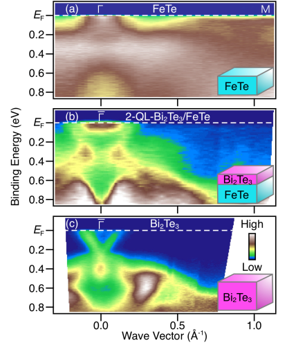
Having established the orientation of Bi2Te3 on FeTe, next we present the electronic states. Figure 2(a) displays the plot of ARPES intensity at = 30 K measured along the M cut of FeTe BZ. One can see three kinds of prominent spectral features; an intense weight in the vicinity of at the point, a broad feature with a relatively flat dispersion at 0.35 eV around the point, and a flat dispersion at the binding energy () of 0.05 eV around the M point. This spectral feature is similar to that of bulk FeTe FeTeARPES1 ; FeTeARPES2 ; FeTeARPES3 , confirming its FeTe origin. Upon fabrication of 2-QL Bi2Te3 film on FeTe, we found a drastic change in the spectral feature. Figure 2(b) shows the ARPES intensity for this heterostructure measured along the same cut as Fig. 2(a), which corresponds to the cut rotated by 15∘ with respect to the / cut of hexagonal Bi2Te3 BZ. This choice of cut simplifies the data interpretation because the band dispersion from the two crystal domains match each other only along this cut. One can immediately recognize from Fig. 2(b) that the broad feature at = 0.3 eV seen in pristine FeTe [Fig. 2(a)] is markedly suppressed. Instead, a new dispersive feature appears at = 0.6-0.8 eV around the point. Since a similar feature is also seen in pristine Bi2Te3 at similar photon energies BiTeARPES1 ; BiTeARPES2 , it is assigned to the Bi2Te3 band. We also find a new holelike band topped at 0.4 eV at the point which is also attributed to the Bi2Te3 band, because a similar band appears in Bi2Te3 on Si(111), as displayed in Fig. 2(c).
While the spectral intensity near away from the point is almost zero in pristine Bi2Te3 [Fig. 2(c)], that in 2-QL-Bi2Te3/FeTe has a finite weight [Fig. 2(b)]. Such feature can be seen in FeTe [Fig. 2(a)], suggesting that a faint photoelectron signal from FeTe beneath 2-QL Bi2Te3 was detected despite significant suppression of the spectral weight. This could be possible because the photoelectron escape depth at this photon energy is 1 nm and as a result about 10 of total photoelectrons escape from FeTe through the 2-QL (2 nm)-thick Bi2Te3. We will show later that the observation of buried electronic states of FeTe is corroborated by a close inspection of spectral signature around the point near . The most important spectral signature of 2-QL-Bi2Te3/FeTe in Fig. 2(b) is that there exists a linearly dispersive band across , reminiscent of the Dirac-cone surface state (SS) in Bi2Te3 in Fig. 2(c). Interestingly, its Fermi vectors appear to be expanded compared to those of pristine Bi2Te3. This change is also responsible for the observed expansion of FS in Figs. 1(f) and 1(g). The experimental fact that the twelve-fold symmetric intensity pattern in Fig. 1(f) originates from the linearly dispersive band in Fig. 2(b) supports that this band is of Dirac-cone SS origin.
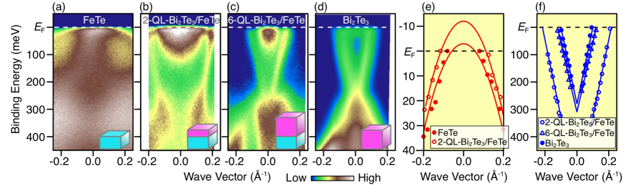
To see more clearly the change in the electronic states upon interfacing Bi2Te3 and FeTe, we show in Fig. 3 the near- ARPES intensity around the point for (a) pristine FeTe (10 ML), (b) 2 and (c) 6 QLs of Bi2Te3 on FeTe, and (d) Bi2Te3 on Si(111), measured with higher statistics and energy resolution. One can see from a side-by-side comparison of Figs. 3(a) and 3(b) that a shallow holelike band that crosses around the point in FeTe [Fig. 3(a)] is still seen even after growth of 2-QL Bi2Te3 on FeTe [Fig. 3(b)], while its intensity is markedly suppressed. On increasing the number of QLs to 6, the holelike band completely disappears [Fig. 3(c)]. This is reasonable since the photoelectrons cannot escape from buried FeTe because Bi2Te3 is too thick ( 6 nm). Another important aspect of Fig. 3 is the Dirac-cone SS. One can see that 6-QL Bi2Te3 on FeTe [Fig. 3(c)] and pristine Bi2Te3 [Fig. 3(d)] shows a similar Dirac-cone feature at similar ’s (note that the conduction band is not clearly seen in pristine Bi2Te3 because the value is not rightly at the conduction-band minimum), whereas that for 2-QL Bi2Te3 on FeTe sinks well below [Fig. 3(b)].
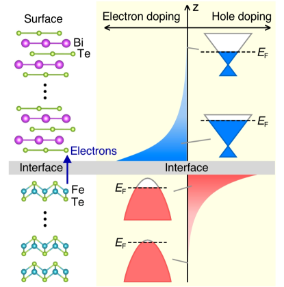
To discuss quantitatively the observed change in the energy bands, we have estimated the energy position of FeTe-originated holelike band by tracing the peak position of energy distribution curves (EDCs), and the result is shown in Fig. 3(e). It is obvious that the shape of band dispersion is quite similar between 2-QL-Bi2Te3/FeTe and pristine FeTe, whereas the former band is shifted as a whole by 10 meV toward lower with respect to the latter one. This indicates that the FeTe surface (interface) is hole-doped upon interfacing the Bi2Te3 layer. By contrast, the downward shift of the Dirac-cone state in 2-QL-Bi2Te3/FeTe compared to pristine Bi2Te3, as clarified in the quantitative analysis of band energies in Fig. 3(f), signifies that the Bi2Te3 layers interfaced with FeTe are electron-doped. A similar energy position of the Dirac cones between 6-QL-Bi2Te3/FeTe and pristine Bi2Te3 shown in Fig. 3(f) implies that extra electron charge is accumulated near the interface. These observations are summarized in the schematic depth profile of band diagram and extra electron/hole charge carriers in Fig. 4. The electron- vs hole-doped nature of Bi2Te3 and FeTe suggests that electron charge transfer from FeTe to Bi2Te3 takes place. This is reasonable since the work function of Bi2Te3 (5.3 eV) BiTeWF is smaller than that of FeTe (4.4 eV) FeTeWF , so that electrons are transferred from FeTe to Bi2Te3 upon making junction.
Now we discuss implications of the present ARPES results in relation to the occurrence of superconductivity. What is fascinating in this heterostructure is that the superconductivity emerges upon junction of non-superconducting Bi2Te3 and FeTe BiTeFeTe1 . There may be two possible explanations for the electronic states responsible for this superconductivity; (i) the Bi2Te3/FeTe interface itself hosts a new band structure different from that of parent materials wherein the superconductivity emerges, or (ii) either carrier-doped Bi2Te3 or FeTe itself becomes superconducting around the interface. The present ARPES result strongly suggests that (i) is unlikely, since all the bands observed in 2-QL-Bi2Te3/FeTe [Figs. 2(b) and 3(b)] can be assigned either to the Bi2Te3- or FeTe-originated bands. Then, the next question is which, electron-doped Bi2Te3 or hole-doped FeTe, or both is superconducting. It is empirically known from previous transport and spectroscopic studies of bulk Bi2Te3 that superconductivity does not emerge by electron-doping by replacement and/or intercalation of atoms. This situation is different from another prototypical topological insulator, Bi2Se3, where intercalation of various atoms (Cu, Nb, and Sr) causes electron-doping and triggers superconductivity CuBiSe ; SrBiSe ; NbBiSe . This naturally leads to a conclusion that electron-doped Bi2Te3 does not host superconductivity. Our result thus implies that the hole-doped FeTe interface is responsible for the superconductivity.
Above consideration naturally favors the scenario that topological superconductivity may take place in Bi2Te3. Assuming that the FeTe interface is superconducting, it would be possible to induce a pairing gap at the Dirac-cone surface/interface state in the QLs of Bi2Te3 by the superconducting proximity effect from FeTe, if the Bi2Te3 film is thick enough to realize the Dirac-cone SSs at the top and bottom surfaces. Since the Dirac-cone band was observed even in the 2-QL-thick Bi2Te3 film BiTeARPES2 , we think that the 2 (and also 6) QL films in the present study can host the spin-helical Dirac-cone states. This would satisfy the theoretically predicted condition of topological superconductivity that utilizes the helical Dirac fermions TSC . A next important challenge is to directly determine the pairing symmetry by measuring the dependence of the proximity-induced gap, and search for a spectroscopic signature of Majorana bound state in the vortex core.
In conclusion, we reported ARPES study on a heterostructure of Bi2Te3 and FeTe epitaxially grown on STO. By comparing the band structure among Bi2Te3/FeTe, FeTe, and Bi2Te3, we found that the electron charge transfer from FeTe to Bi2Te3 takes place upon interfacing Bi2Te3 with FeTe. Moreover, the influence of charge transfer was found to be more prominent for a thinner Bi2Te3 film, suggesting the charge accumulation near the interface. Taking into account that electron-doped Bi2Te3 is unlikely to be a superconductor, we suggested that hole-doped FeTe at the interface is responsible for the occurrence of superconductivity in the heterostructure. This points to possible topological superconductivity occurring at the Dirac-cone surface/interface states in Bi2Te3.
Acknowledgements.
We thank Masato Kuno and Takumi Sato for their assistance in the ARPES experiments. This work was supported by JST-PRESTO (No: JPMJPR18L7), JST-CREST (No: JPMJCR18T1), MEXT of Japan (Innovative Area“Topological Materials Science” JP15H05853), JSPS (JSPS KAKENHI No: JP17H04847, JP17H01139, and JP18H01160), and KEK-PF (Proposal number: 2018S2-001).References
- (1) A. Ohtomo and H. Y. Hwang, Nature 427, 423 (2004).
- (2) N. Reyren, S. Thiel, A. D. Caviglia, L. Fitting-Kourkoutis, G. Hammer, C. Richter, C. W. Schneider, T. Kopp, A.-S. Rüuetschi, D. Jaccard, M. Gabay, D. A. Muller, J.-M. Triscone, and J. Mannhart, Science 317, 1196 (2007).
- (3) Q. Y. Wang, Z. Li, W.-H. Zhang, Z.-C. Zhang, J.-S. Zhang, W. Li, H. Ding, Y.-B. Ou, P. Deng, K. Chang, J. Wen, C.-L. Song, K. He, J.-F. Jia, S.-H. Ji, Y.-Y. Wang, L.-L. Wang, X. Chen, X.-C. Ma, and Q.-K. Xue, Chin. Phys. Lett. 29, 037402 (2012).
- (4) S. He, J. He, W. Zhang, L. Zhao, D. Liu, X. Liu, D. Mou, Y.-B. Ou, Q.-Y. Wang, Z. Li, L. Wang, Y. Peng, Y. Liu, C. Chen, L. Yu, G. Liu, X. Dong, J. Zhang, C. Chen, Z. Xu, X. Chen, X. Ma, Q.-K. Xue, and X. J. Zhou, Nature Mater. 12, 605 (2013).
- (5) S. Tan, Y. Zhang, M. Xia, Z. Ye, F. Chen, X. Xie, R. Peng, D. Xu, Q. Fan, H. Xu, J. Jiang, T. Zhang, X. Lai, T. Xiang, J. Hu, B. Xie, and D. Feng, Nature Mater. 12, 634 (2013).
- (6) Q. L. He, H. Liu, M. He, Y. H. Lai, H. He, G. Wang, K. T. Law, R. Lortz, J. Wang, and I. K. Sou, Nature Commun. 5, 4247 (2014).
- (7) G. Du, Z. Du, X. Yang, E. Wang, D. Fang, H. Yang, and H.-H. Wen, ArXiv:1509.07424.
- (8) M. N. Kunchur, C. L. Dean, N. S. Moghadam, J. M. Knight, Q. L. He, H. Liu, J. Wang, R. Lortz, I. K. Sou, and A. Gurevich, Phys. Rev. B 92, 094502 (2015).
- (9) Q. L. He, M. He, J. Shen, Y. H. Lai, Y. Liu, H. Liu, H. He, G. Wang, J. Wang, R. Lortz, and I. K. Sou, J. Phys.: Condens. Matter 27, 345701 (2015).
- (10) H.-C. Liu, H. Li, Q. L. He, I. K. Sou, S. K. Goh, and J. Wang, Sci. Rep. 6, 26168 (2016).
- (11) M. Q. He, J. Y. Shen, A. P. Petrović, Q. L. He, H. C. Liu, Y. Zheng, C. H. Wong, Q. H. Chen, J. N. Wang, K. T. Law, I. K. Sou, and R. Lortz, Sci. Rep. 6, 32508 (2016).
- (12) J. Shen, C. Heuckeroth, Y. Deng, Q. He, H. C. Liu, J. Liang, J. Wang, I. K. Sou, J. S. Schilling, and R. Lortza, Physica C 543, 18 (2017).
- (13) Y. Xia, D. Qian, L. Wray, D. Hsieh, G. F. Chen, J. L. Luo, N. L. Wang, and M. Z. Hasan, Phys. Rev. Lett. 103, 037002 (2009).
- (14) Y. Zhang, F. Chen, C. He, L. X. Yang, B. P. Xie, Y. L. Xie, X. H. Chen, M. Fang, M. Arita, K. Shimada, H. Namatame, M. Taniguchi, J. P. Hu, and D. L. Feng, Phys. Rev. B 82, 165113 (2010).
- (15) E. Ieki, K. Nakayama, Y. Miyata, T. Sato, H. Miao, N. Xu, X.-P. Wang, P. Zhang, T. Qian, P. Richard, Z.-J. Xu, J. S. Wen, G. D. Gu, H. Q. Luo, H.-H. Wen, H. Ding, and T. Takahashi, Phys. Rev. B 89, 140506(R) (2014).
- (16) Y. L. Chen, J. G. Analytis, J.-H. Chu, Z. K. Liu, S.-K. Mo, X. L. Qi, H. J. Zhang, D. H. Lu, X. Dai, Z. Fang, S. C. Zhang, I. R. Fisher, Z. Hussain, and Z.-X. Shen, Science 325, 178 (2009).
- (17) Y.-Y. Li, G. Wang, X.-G. Zhu, M.-H. Liu, C. Ye, X. Chen, Y.-Y. Wang, K. He, L.-L. Wang, X.-C. Ma, H.-J. Zhang, X. Dai, Z. Fang, X.-C. Xie, Y. Liu, X.-L. Qi, J.-F. Jia, S.-C. Zhang, and Q.-K. Xue. Adv. Mater. 22, 4002 (2010).
- (18) D. Takane, S. Souma, T. Sato, T. Takahashi, K. Segawa, and Y. Ando, Appl. Phys. Lett. 109, 091601 (2016).
- (19) M. Kuno ., in preparation.
- (20) Y. S. Hor, A. J. Williams, J. G. Checkelsky, P. Roushan, J. Seo, Q. Xu, H. W. Zandbergen, A. Yazdani, N. P. Ong, and R. J. Cava, Phys. Rev. Lett. 104, 057001 (2010).
- (21) Z. Liu, X. Yao, J. Shao, M. Zuo, L. Pi, S. Tan, C. Zhang, and Y. Zhang, J. Am. Chem. Soc. 137, 10512 (2015).
- (22) T. Asaba, B.-J. Lawson, C. Tinsman, L. Chen, P. Corbae, G. Li, Y. Qiu, Y.-S. Hor, L. Fu, and L. Li, Phys. Rev. X 7, 011009 (2017).
- (23) L. Fu and C. L. Kane, Phys. Rev. Lett. 100, 096407 (2008).