Conductance-matrix symmetries of a three-terminal hybrid device
Abstract
We present conductance-matrix measurements of a three-terminal superconductor-semiconductor hybrid device consisting of two normal leads and one superconducting lead. Using a symmetry decomposition of the conductance, we find that the antisymmetric components of pairs of local and nonlocal conductances match at energies below the superconducting gap, consistent with expectations based on a non-interacting scattering matrix approach. Further, the local charge character of Andreev bound states is extracted from the symmetry-decomposed conductance data and is found to be similar at both ends of the device and tunable with gate voltage. Finally, we measure the conductance matrix as a function of magnetic field and identify correlated splittings in low-energy features, demonstrating how conductance-matrix measurements can complement traditional tunneling-probe measurements in the search for Majorana zero modes.
pacs:
03.67.Lx, 81.07.Gf, 85.25.CpSymmetry relations for quantum transport are often connected to deep physical principles, and make strong predictions for comparison with experiment. For instance, the Onsager-Casimir relations Onsager (1931); Casimir (1945); Büttiker (1988) arise from microscopic reversibility, and were central in early studies of quantum-coherent transport Webb et al. (1985); Benoit et al. (1986); Büttiker (1986). Later, predicted departures from these relations due to interaction effects Christen and B√ºttiker (1996); Spivak and Zyuzin (2004); Sánchez and Büttiker (2004), which include bias-dependence of the effective potentials, were observed in nonlinear transport Löfgren et al. (2004); Zumbühl et al. (2006). The introduction of superconducting terminals results in additional symmetries, as conductance occurs via Andreev-reflection from electrons to holes, and is invariant under particle-hole conjugation Andreev (1964). For a two-terminal normal-superconducting device, the conductance, , is a symmetric function of bias voltage, , neglecting interaction effects. As shown in a partner theoretical paper, for multi-terminal superconducting devices need not be symmetric, although a curious relation exists between the antisymmetric components of the local and nonlocal conductances Danon et al. (2019). These predictions have, to our knowledge, not been tested.
Hybrid superconductor-semiconductor nanowire structures have recently become a topic of intense interest Mourik et al. (2012); Das et al. (2012); Churchill et al. (2013); Albrecht et al. (2016); Deng et al. (2016); Zhang et al. (2018), motivated in part by proposals for achieving topological superconductivity and Majorana zero modes (MZM) Lutchyn et al. (2010); Oreg et al. (2010). In two-terminal superconductor-semiconductor devices, observed asymmetries in the subgap conductance Gül et al. (2018) have been suggested to arise from a dissipative fermionic reservoir, effectively acting as a third lead Liu et al. (2017a), although, as in the normal-conducting case Büttiker (1988), bias-dependence of the self-consistent potential can also cause a deviation from symmetry Chen et al. (2017). Multi-terminal superconducting devices are a topic of particular interest, as they can be used for MZM Das Sarma et al. (2012); Fregoso et al. (2013); Stanescu and Tewari (2014); Rosdahl et al. (2018); Reeg et al. (2018); Lai et al. (2019); Anselmetti et al. (2019), Cooper-pair splitter Hofstetter et al. (2009); Herrmann et al. (2010), and multi-terminal Josephson studies van Heck et al. (2014); Strambini et al. (2016); Meyer and Houzet (2017); Xie et al. (2017); Pankratova et al. (2018). In multi-terminal superconducting quantum dot devices, bias asymmetries have been observed Hofstetter et al. (2011), and a relationship between nonlocal conductance and the bound-state charge has been proposed Schindele et al. (2014); Gramich et al. (2017).
In this Letter, we report a symmetry analysis of the conductance matrix measured in a three-terminal, superconductor-semiconductor hybrid device. The antisymmetric components for pairs of conductance matrix elements are found to coincide at energies below the superconducting gap. We use the symmetry-decomposed nonlocal conductance to extract the local charge character of states within the superconducting gap as a function of gate voltage, discovering that the charge is approximately equal on both sides of the device. Finally, we measure local and nonlocal conductances at nonzero magnetic field and identify isolated low-energy states with correlated splittings on each end of the wire, using inferred charge as an additional spectroscopic tool for comparison with theory. This work provides new methods for studying the local charge density of subgap bound states and distinguishing between topological and trivial states. More generally, it provides a better understanding of the role of symmetry in multi-terminal superconducting quantum devices.
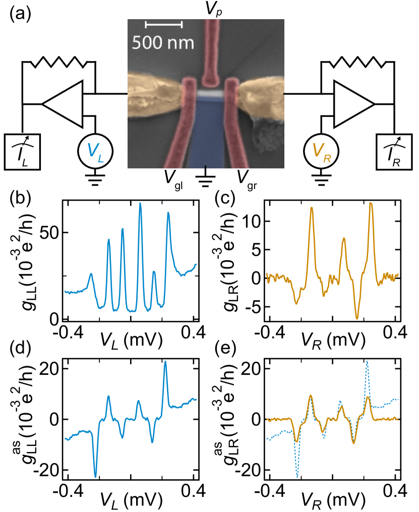
Selective area growth (SAG) of InAs nanowires Krizek et al. (2018); Vaitiekėnas et al. (2018) is preformed by chemical beam epitaxy (CBE) on an InP substrate masked with silicon oxide Lee (2018). The nanowire is half-covered by an Al film, which was deposited in-situ after CBE growth, and is selectively etched to form a superconducting lead. The device consists of two normal Ti/Au electrodes (yellow), a central semiconducting region proximitized by Al (blue), a global HfOx dielectric layer, and Ti/Au electrostatic gates (red). We emphasize that the superconducting lead is deposited during growth and contacted remote from the delicate superconductor-semiconductor interface, a benefit of the SAG approach.
Conductance is measured by applying a DC bias voltage and an AC voltage at the right (left) terminal with two different AC excitation frequencies 18 Hz and 42 Hz. The in-phase AC current flowing to the right (left) side is measured with the middle superconducting lead grounded. The device is tunnel-coupled to the normal leads by adjusting the two tunnel-gate voltages and such that e2/h, which also ensures that the applied voltages drop over the tunnel barriers. We have checked for spurious voltage divider effects using a four-probe measurement on a cold-grounded device, and do not find deviations from the data presented here. The plunger gate voltage is used to tune the chemical potential of the semiconductor. All measurements are performed at base temperature of a dilution refrigerator.
The experimental setup allows the measurement of the conductance matrix
| (1) |
where the sign convention is chosen for compatibility with standard two-terminal measurements of .
Figure 1(b) shows as a function of with . Several peaks occur symmetrically around zero bias. We assign the two highest energy peaks to coherence peaks, a signature of the Bardeen-Cooper-Schrieffer (BCS) density of states in the proximitized semiconductor with an induced gap 250 eV, in agreement with previous observation for similar material systems Chang et al. (2015); Vaitiekėnas et al. (2018). The other peaks are subgap states with energies . Both the high-bias conductance () as well as the subgap peak heights are asymmetric in bias [Fig. 1(b)]. The nonlocal conductance , measured as function of with in Fig. 1(c), exhibits features corresponding to the peaks in . The sign of the peak amplitudes in , however, changes with a sign-change in bias, indicating a strong odd component. The remaining conductance-matrix elements and were also measured and exhibit similar features 111See supplement.
To further explore the symmetry properties, the conductance traces are decomposed into their symmetric,
| (2) |
and antisymmetric,
| (3) |
parts. Figure 1(d) shows as a function of , which bears a qualitative resemblance to . In fact, , the antisymmetric component of , closely matches [dashed line in Fig. 1(e)] for low bias, with some quantitative departures observed at high bias. Reference Danon et al. (2019) discusses the identified symmetry relation, , as an underlying symmetry of the scattering matrix for . Departures from this symmetry can result from bias-voltage dependence of the effective potentials Büttiker (1988), single-particle scattering into the nominally superconducting lead Danon et al. (2019), or inelastic processes within the hybrid region Liu et al. (2017a). The fact that departures from symmetry smoothly scale with bias voltage would seem to favor an explanation based on bias-dependent potentials. In addition, we have found that the observed symmetry departures have relatively little field-dependence, suggesting that they are not due to the presence of dissipation from vortices.
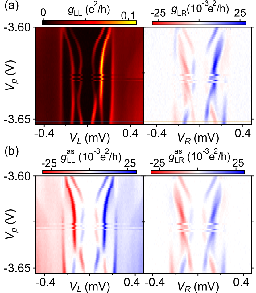
Next, we investigate the conductance matrix as a function of gate voltage. Figure 2(a) shows () as a function of and bias (). makes the assignment of coherence peaks and subgap states more clear. The coherence peaks do not move when changing the gate voltage, while subgap states appear at different bias voltages for different . We attribute these subgap states to Andreev bound states (ABS), although it is not entirely clear where the states are confined. We speculate that confinement could result from a Fermi velocity mismatch between the InAs and the Al or disorder in the system. The ABS subgap features are visible as peaks in the nonlocal conductance as well. Pairs of ABS resonances at positive and negative bias are found to have opposite sign, again indicating a primarily odd functional form. Symmetry-decomposing the datasets as a function of bias yields and [Fig. 2(b)], which show a remarkable correspondence in general, indicating that the symmetry relationship identified in Fig. 1 is robust as a function of gate voltage. However, in addition to the quantitative high-bias discrepancies already identified in Fig. 1(e), there are isolated regions in Fig. 2(b) where and qualitatively differ, associated with crossing of subgap states, e.g. around ; these regions are presently not understood.
It is interesting to note that ABS with the same slope with respect to have the same sign in . Further, where the slope changes sign, i.e. at inflection points, the nonlocal conductance disappears and changes sign as well [Fig. 2(a)]. Reference Danon et al. (2019) shows that, for a spectrally isolated subgap state at energy , the sign of the nonlocal conductance at bias voltages near is generally related to the state’s local charge density. The symmetric part of the conductance, for a bound state coupled to the left(right) leads at rate and energy is
| (4) |
and the antisymmetric part is
| (5) |
where is the local charge density, is the local probability density, and , are the left (right) Bogoliubov-de Gennes (BdG) amplitudes. The general expression for is cumbersome, but in the limiting case it takes the simple form . Similar expressions also hold for . As a consequence, there is a proportionality between the symmetry-decomposed nonlocal conductance and the local charge densities, and .
Proportionality constants can be eliminated by considering the ratio of conductances,
| (6) | |||||
| (7) |
is a measure of the local charge character; for a state that is locally electron-like (), and for a state that is locally hole-like ().
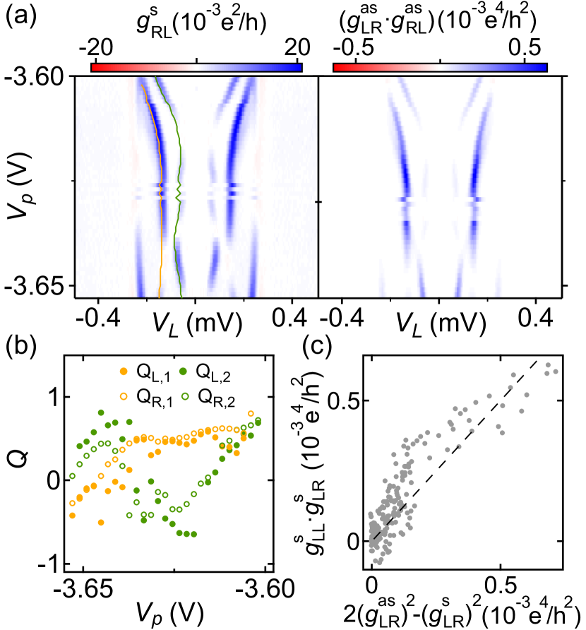
Motivated by these theoretical relations, we compare in Fig. 3(a) the measured symmetric component of a single nonlocal conductance, , with the product of the antisymmetric components of both nonlocal conductances, . The plots in Fig. 3(a) are qualitatively similar, as expected from Eqs. (4-5), and suggesting that gate dependence of the BCS charge has a dominant effect on the conductance of subgap peaks. To further explore the charge of subgap states, the data are analyzed by extracting peak positions of the ABS resonances from . Decompositions of the nonlocal conductance are evaluated at these positions to obtain and . is calculated from the peak values for two different subgap states [orange and green lines in Fig. 3(a)]. The local charge character for these states oscillates as a function of , highlighting the gate-tunable charge character of bound state [orange and green markers in Fig. 3(b)]. Sign changes of indicate that the state is changing from electron-like to a hole-like, or vice versa. We note that the sign changes of are given by the sign changes of . Hence the earlier observations that ABS with the same slope with respect to have the same sign in and change sign at inflection points is entirely consistent with the charge interpretation. Using , can be analogously calculated [open markers in Fig. 3(b)], and it is found to be similar to for both bound states.
The similarity between and suggests that the BdG amplitudes have a weak spatial dependence. In theory, when and are spatially uniform Ref. Danon et al. (2019) predicts that a symmetry relation emerges,
| (8) |
A parametric plot of the left-side versus right-side of Eq. (8) for all identified peaks in the dataset reveals that these quantities are approximately equal [Fig. 3(c)], supporting the view that the coherence factors are spatially uniform. Indeed, performing a linear fit of the data gives a slope of with a small intercept , indicating a good general agreement with the relationship predicted by Eq. (8). However, there are regions of gate voltage where this analysis systematically fails, such as the previously discussed region , where feature crossings are observed in .

Having established the nonlocal conductance as a tool for characterizing subgap states, we now apply a magnetic field while measuring the conductance matrix. Figures 4(a) and (d) show the evolution of and in a magnetic field applied parallel to the wire. The ABS evolve as a function of as detected from both ends of the device. As the field initially increases, the low-lying states split and anticross, eventually merging at zero energy. For further increases in field, the low energy states oscillate around zero energy, a signature typically attributed to hybridized MZM in devices comparable in length to the coherence length Albrecht et al. (2016). The correlated splitting of zero-bias peaks, measured from both wires ends, was proposed as a “smoking gun” signature of MZM Das Sarma et al. (2012), but given the presence of strong correlations at zero magnetic field in this device Anselmetti et al. (2019), we suggest that this signature is not by itself conclusive.
The nonlocal conductances and [Figs. 4(b) and (c)] as a function of field have asymmetric features corresponding to subgap states in the local conductance, and also exhibit several changes in sign. To study the sign of for the low-energy features, peaks in the local conductance, , are determined [orange line Fig. 4(c)], and the peak nonlocal conductance, , is extracted at these points. Of particular interest is the behavior at the field T, where the energy of the oscillating states has a turning point. The nonlocal conductance at is nonzero [Fig. 4(e)], inconsistent with the expect behavior for hybridized MZM, which are chargeless at turning points and therefore have vanishing nonlocal conductance Hansen et al. (2018); Danon et al. (2019). Interestingly, at a higher field , there is a second turning point where the nonlocal conductance is small, consistent with the behavior expected for chargeless, hybridized MZM 222At , has large error bars due to small signal, but from Eqs. (4-5), implies for nonzero couplings.. The non-local transport data therefore reveal the presence of effects outside of the Luchyn-Oreg model Lutchyn et al. (2010); Oreg et al. (2010) at intermediate fields (). Intermediate-field effects in hybrid nanowires, in particular the possibility of quasi-Majorana modes that emerge before the true topological transition Liu et al. (2017b); Vuik et al. (2018); Reeg et al. (2018), have been discussed at length in the literature. It is, to the best of our knowledge, an open theoretical problem to check if quasi-Majoranas, or other effects Domínguez et al. (2017), can explain the anomalous charge character that we have inferred near .
In summary, the observed symmetry relations are consistent with a non-interacting scattering picture, and justify the use of symmetry-decomposed conductance to infer the BCS charge. At finite field, we have observed correlated splittings of zero-bias peaks, but find that at intermediate fields their charge character is not consistent with a simple Majorana picture. We anticipate that tunneling spectroscopy at both wire ends, combined with the insights from the nonlocal conductance, will play an important role in substantiating the existence of MZM.
Acknowledgements.
We acknowledge helpful discussions with Jeroen Danon, Roman Lutchyn, Dima Pikulin, and Torsten Karzig. This work was supported by Microsoft Project Q and the Danish National Research Foundation. C.M.M. acknowledges support from the Villum Foundation.References
- Onsager (1931) L. Onsager, Phys. Rev. 38, 2265 (1931).
- Casimir (1945) H. B. G. Casimir, Rev. Mod. Phys. 17, 343 (1945).
- Büttiker (1988) M. Büttiker, IBM J. Res. Dev. 32, 317 (1988).
- Webb et al. (1985) R. A. Webb, S. Washburn, C. P. Umbach, and R. B. Laibowitz, Phys. Rev. Lett. 54, 2696 (1985).
- Benoit et al. (1986) A. D. Benoit, S. Washburn, C. P. Umbach, R. B. Laibowitz, and R. A. Webb, Phys. Rev. Lett. 57, 1765 (1986).
- Büttiker (1986) M. Büttiker, Phys. Rev. Lett. 57, 1761 (1986).
- Christen and Büttiker (1996) T. Christen and M. Büttiker, Eur. Phys. Lett. 35, 523 (1996).
- Spivak and Zyuzin (2004) B. Spivak and A. Zyuzin, Phys. Rev. Lett. 93, 226801 (2004).
- Sánchez and Büttiker (2004) D. Sánchez and M. Büttiker, Phys. Rev. Lett. 93, 106802 (2004).
- Löfgren et al. (2004) A. Löfgren, C. A. Marlow, I. Shorubalko, R. P. Taylor, P. Omling, L. Samuelson, and H. Linke, Phys. Rev. Lett. 92, 046803 (2004).
- Zumbühl et al. (2006) D. M. Zumbühl, C. M. Marcus, M. P. Hanson, and A. C. Gossard, Phys. Rev. Lett. 96, 206802 (2006).
- Andreev (1964) A. F. Andreev, Sov. Phys. JETP 19, 1228 (1964).
- Danon et al. (2019) J. Danon, A. B. Hellenes, E. B. Hansen, L. Casparis, A. P. Higginbotham, and K. Flensberg, Submitted (2019).
- Mourik et al. (2012) V. Mourik, K. Zuo, S. M. Frolov, S. R. Plissard, E. P. A. M. Bakkers, and L. P. Kouwenhoven, Science 336, 1003 (2012).
- Das et al. (2012) A. Das, Y. Ronen, Y. Most, Y. Oreg, M. Heiblum, and H. Shtrikman, Nat. Phys 8, 887 (2012).
- Churchill et al. (2013) H. O. H. Churchill, V. Fatemi, K. Grove-Rasmussen, M. T. Deng, P. Caroff, H. Q. Xu, and C. M. Marcus, Phys. Rev. B 87, 241401(R) (2013).
- Albrecht et al. (2016) S. M. Albrecht, A. Higginbotham, M. Madsen, F. Kuemmeth, T. S. Jespersen, J. Nygård, P. Krogstrup, and C. M. Marcus, Nature 531, 206 (2016).
- Deng et al. (2016) M. T. Deng, S. Vaitiekenas, E. B. Hansen, J. Danon, M. Leijnse, K. Flensberg, J. Nygård, P. Krogstrup, and C. M. Marcus, Science 354, 1557 (2016).
- Zhang et al. (2018) H. Zhang, C.-X. Liu, S. Gazibegovic, D. Xu, J. A. Logan, G. Wang, N. van Loo, J. D. S. Bommer, M. W. A. de Moor, D. Car, R. L. M. Op het Veld, P. J. van Veldhoven, S. Koelling, M. A. Verheijen, M. Pendharkar, D. J. Pennachio, B. Shojaei, J. S. Lee, C. J. Palmstrøm, E. P. A. M. Bakkers, S. Das Sarma, and L. P. Kouwenhoven, Nature 556, 74–79 (2018).
- Lutchyn et al. (2010) R. M. Lutchyn, J. D. Sau, and S. Das Sarma, Phys. Rev. Lett. 105, 077001 (2010).
- Oreg et al. (2010) Y. Oreg, G. Refael, and F. von Oppen, Phys. Rev. Lett. 105, 177002 (2010).
- Gül et al. (2018) Ö. Gül, H. Zhang, J. D. S. Bommer, M. W. A. de Moor, D. Car, S. R. Plissard, E. P. A. M. Bakkers, A. Geresdi, K. Watanabe, T. Taniguchi, and L. P. Kouwenhoven, Nature Nanotechnology 13, 192 (2018).
- Liu et al. (2017a) C.-X. Liu, J. D. Sau, and S. Das Sarma, Phys. Rev. B 95, 054502 (2017a).
- Chen et al. (2017) J. Chen, P. Yu, J. Stenger, M. Hocevar, D. Car, S. R. Plissard, E. P. A. M. Bakkers, T. D. Stanescu, and S. M. Frolov, Science Advances 3 (2017).
- Das Sarma et al. (2012) S. Das Sarma, J. D. Sau, and T. D. Stanescu, Phys. Rev. B 86, 220506(R) (2012).
- Fregoso et al. (2013) B. M. Fregoso, A. M. Lobos, and S. Das Sarma, Phys. Rev. B 88, 180507(R) (2013).
- Stanescu and Tewari (2014) T. D. Stanescu and S. Tewari, Phys. Rev. B 89, 220507(R) (2014).
- Rosdahl et al. (2018) T. O. Rosdahl, A. Vuik, M. Kjaergaard, and A. R. Akhmerov, Phys. Rev. B 97, 045421 (2018).
- Reeg et al. (2018) C. Reeg, O. Dmytruk, D. Chevallier, D. Loss, and J. Klinovaja, Phys. Rev. B 98, 245407 (2018).
- Lai et al. (2019) Y.-H. Lai, J. D. Sau, and S. Das Sarma, arxiv:1901.02655 (2019).
- Anselmetti et al. (2019) G. L. R. Anselmetti, E. A. Martinez, G. C. Méenard, D. Puglia, F. K. Malinowski, J. Lee, S. Choi, M. Pendharkar, C. J. Palmstrøm, C. M. Marcus, L. Casparis, and A. P. Higginbotham, Submitted (2019).
- Hofstetter et al. (2009) L. Hofstetter, S. Csonka, J. Nygård, and C. Schönenberger, Nature 461, 960 (2009).
- Herrmann et al. (2010) L. G. Herrmann, F. Portier, P. Roche, A. L. Yeyati, T. Kontos, and C. Strunk, Phys. Rev. Lett. 104, 026801 (2010).
- van Heck et al. (2014) B. van Heck, S. Mi, and A. R. Akhmerov, Phys. Rev. B 90, 155450 (2014).
- Strambini et al. (2016) E. Strambini, S. D’Ambrosio, F. Vischi, F. S. Bergeret, Y. V. Nazarov, and F. Giazotto, Nature Nanotechnology 11, 1055 (2016).
- Meyer and Houzet (2017) J. S. Meyer and M. Houzet, Phys. Rev. Lett. 119, 136807 (2017).
- Xie et al. (2017) H.-Y. Xie, M. G. Vavilov, and A. Levchenko, Phys. Rev. B 96, 161406(R) (2017).
- Pankratova et al. (2018) N. Pankratova, H. Lee, R. Kuzmin, M. Vavilov, K. Wickramasinghe, W. Mayer, J. Yuan, J. Shabani, and V. E. M. Manucharyan, arXiv:1812.06017 (2018).
- Hofstetter et al. (2011) L. Hofstetter, S. Csonka, A. Baumgartner, G. Fülöp, S. d’Hollosy, J. Nygård, and C. Schönenberger, Phys. Rev. Lett. 107, 136801 (2011).
- Schindele et al. (2014) J. Schindele, A. Baumgartner, R. Maurand, M. Weiss, and C. Schönenberger, Phys. Rev. B 89 (2014).
- Gramich et al. (2017) J. Gramich, A. Baumgartner, and C. Schönenberger, Phys. Rev. B 96, 195418 (2017).
- Krizek et al. (2018) F. Krizek, J. E. Sestoft, P. Aseev, S. Marti-Sanchez, S. Vaitiekėnas, L. Casparis, S. A. Khan, Y. Liu, T. Stankevič, A. M. Whiticar, A. Fursina, F. Boekhout, R. Koops, E. Uccelli, L. P. Kouwenhoven, C. M. Marcus, J. Arbiol, and P. Krogstrup, Phys. Rev. Materials 2, 093401 (2018).
- Vaitiekėnas et al. (2018) S. Vaitiekėnas, A. M. Whiticar, M.-T. Deng, F. Krizek, J. E. Sestoft, C. J. Palmstrøm, S. Marti-Sanchez, J. Arbiol, P. Krogstrup, L. Casparis, and C. M. Marcus, Phys. Rev. Lett. 121, 147701 (2018).
- Lee (2018) J. S. e. a. Lee, arXiv preprint arXiv:1808.04563 (2018).
- Chang et al. (2015) W. Chang, S. M. Albrecht, T. S. Jespersen, F. Kuemmeth, P. Krogstrup, J. Nygård, and C. M. Marcus, Nature Nanotechnology 10, 232 (2015).
- Note (1) See supplement.
- Hansen et al. (2018) E. B. Hansen, J. Danon, and K. Flensberg, Phys. Rev. B 97, 041411(R) (2018).
- Note (2) At , has large error bars due to small signal, but from Eqs. (4-5), implies for nonzero couplings.
- Liu et al. (2017b) C.-X. Liu, J. D. Sau, T. D. Stanescu, and S. Das Sarma, Phys. Rev. B 96, 075161 (2017b).
- Vuik et al. (2018) A. Vuik, B. Nijholt, A. R. Akhmerov, and M. Wimmer, arXiv e-prints (2018), arXiv:1806.02801 [cond-mat.mes-hall] .
- Domínguez et al. (2017) F. Domínguez, J. Cayao, P. San-Jose, R. Aguado, A. L. Yeyati, and E. Prada, npj Quantum Materials 2 (2017), 10.1038/s41535-017-0012-0.