Unconventional domain wall magnetoresistance of patterned Ni/Nb bilayer structures below superconducting transition temperature of Nb
Abstract
Scattering of spin-up and spin-down electrons while passing through a ferromagnetic domain wall leads to an additional resistance for transport current, usually observed prominently in constricted magnetic structures. In this report we use the resistance of the domain wall as a probe to find an indirect signatures of the theoretically predicted spin-singlet supercurrent to spin-triplet supercurrent conversion effect of ferromagnetic domain walls. Here we examine the domain wall induced resistance in Ni stripe in a bilayer Ni/Nb geometry in the normal state and in the superconducting state of Nb. By making a 6m wide gap in the top Nb layer we routed the transport current through the Ni layer in the normal state and in the supercondcuting state of Nb. In the normal state of Nb, in-field transport measurements showed a clear domain wall magneto-resistance (DWMR) peak near the coercive field, where the domain wall density is expected to be maximum. Interestingly, however, below the superconducting transition temperature of Nb, the DWMR peak of the Ni layer showed a sharp drop in the field range where the number of domain walls become maximum. This observation may be a possible signature of magnetic domain wall induced spin-triplet correlations in the Ni layer due to the direct injection of spin-singlet Cooper pairs from Nb into the magnetic domain walls.
I Introduction
Spin singlet Cooper pairs, when injected across a superconductor(S)-ferromagnet(F) interface, decay within a distance of a few nm in the ferromagnet due to the strong magnetic exchange experienced by the Cooper pairs2 . Therefore, a complete synergy between superconductor and spintronics3 ; 4 is possible only through the generation of long-range, spin triplet Cooper pairs at carefully engineered S-F interfaces. It has been predicted more than a decade ago that magnetic inhomogeneity at the S-F interface is the key ingredient for generation of triplet supercurrent7 from singlet supercurrent. In S-F systems with homogeneous ferromagnetic interface, Cooper pairs undergo spin mixing 3 ; 4 giving rise to short range Sz = 0 singlet and triplet components with a proximity length of the order of 1 to 10 nm. Introduction of magnetization non-collinearity at the S-F interface leads to spin rotation3 ; 4 along with spin mixing which converts short range Sz = 0 triplet component into the long range Sz = 1 triplet component. When a Cooper pair with Sz = 1 triplet component propagates through a ferromagnetic layer, the exchange field of ferromagnet no longer has a pair-breaking effect on it3 ; 4 .
In this direction, a long range supercurrent was reported in Josephson junctions with half metallic ferromagnetic CrO2 barriers10 . However, the results were less reproducible due to the random nature of inhomogeneous magnetic states at the SF interface. Later on, a series of experiments were reported demonstrating the generation of triplet supercurrent in SFS Josephson junctions by carefully engineering the SF interface to be magnetically inhomogeneous11 ; 12 ; 14 ; 17 . Recently, a series of experiments have been carried out to generate triplet supercurrent in Josephson junctions with textured ferromagnets22 , bilayer and trilayer ferromagnetic regions24 , spin injection25 , and via spin-active interfaces26 , by creating a misalignment of magnetic moments at the SF interface. Evidences of induced triplet superconductivity have also been reported using scanning tunneling spectroscopy of SF bilayers27 , Andreev spectroscopy in SF junctions28 , conductance measurements28 , and critical temperature measurements of S-F spin-valve33 . In a recent report by Robinson et al.36 , an in-plane Bloch domain wall was created artificially in Gd by using non-parallel alignment of the Ni layer moments in a Ni-Gd-Ni trilayer in the Nb-Ni-Gd-Ni-Nb Josephson junction. An enhancement of supercurrent was observed in this structure by modifying the low temperature DW state in Gd. The magnetic inhomogeneity has been created artificially in all these reports. However, theoretically, a magnetic domain wall (DW) at the SF interface should also be able to produce triplet Cooper-pairs34 ; 35 ; 7 ; 4 . The fundamental difficulty in implementing this concept is that a domain wall exists only at the interface of two ferro-magnetic domains. In order to utilize the domain wall as a singlet to triplet converter, singlet Cooper pairs need to be passed from one side of the domain wall to the other side, whereas the ferromagnetic exchange field in the domains forbids the presence of spin-singlet Cooper pairs.
In this report, we have tried to inject spin-singlet Cooper pairs directly into the domain walls of a ferromagnetic layer from a superconducting layer deposited on top of the ferromagnetic layer in a bilayer stripe geometry as shown in Fig. 1(a). It is well known 38 that domain walls in a ferromagnet add a resistance to the overall resistance of the ferromagnetic layer. This domain wall magnetoresistance (DWMR) becomes maximum in the magnetic field range where the number of domain walls maximizes. We find that in the normal state of the Nb layer the usual domain wall magnetoresistance appears superposed on the anisotropic magnetoresistance of Ni layer. However, in the superconducting state of Nb we observe an unconventional decrease in DWMR in the field range where the number of domain walls become maximum. This observation may be a signature of the singlet-triplet conversion effect of the domain walls.
II Experimental Details
Nb-Ni thin films with thickness of 55 nm and 100 nm were prepared at room temperature using dc-magnetron sputtering of high purity() niobium and nickel targets on cleaned Si-SiO2 substrates. Deposition of the films was carried out at a base pressure of mBar in an ultra high vacuum chamber. Optical lithography and reactive ion etching techniques were used to fabricate the Nb-Ni-Nb planar structures as shown in Fig 1 (a) . Four probe electrical transport measurements were carried out using a liquid cryogen free dewar. The voltage was measured by reversing the current and averaging over five measurements. The temperature was stable within a range of 3 mK. Magnetization measurements were carried out using vibrating sample magnetometer. The magnetic domains in patterned structures were imaged by magneto-optical Kerr microscope in longitudinal mode for an in-plane magnetic field applied along the length and width of the stripes.
III Results
III.1 Domain wall magneto-resistance in Nb/Ni stripes in the normal state of Nb:
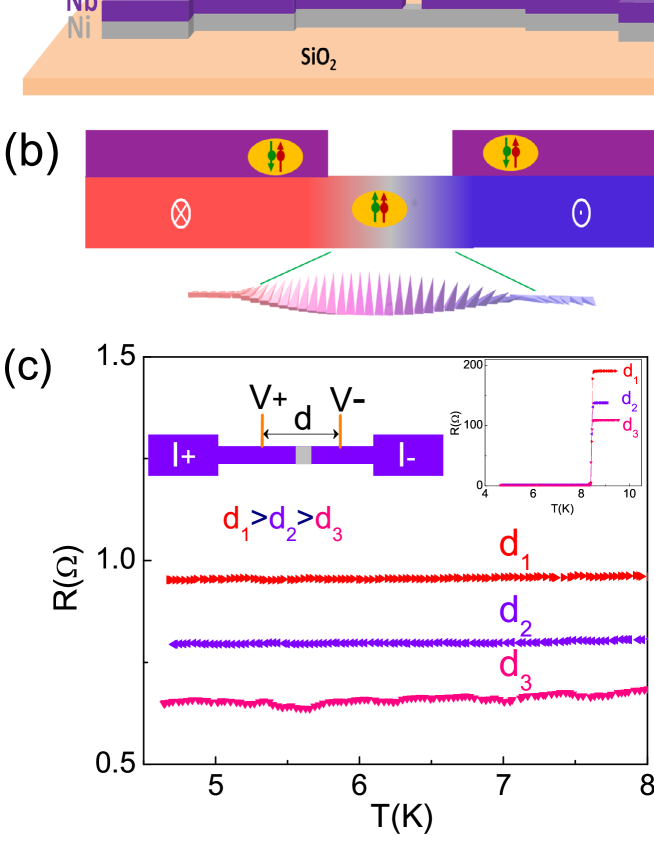
We have lithographically patterned stripes of width 6 m from Ni/Nb bilayer thin films as shown in the schematic of Fig.1(a). Ni has been chosen as the ferromagnet layer because of its high exchange field and the consequent low singlet pair coherence length (4 nm)54 . The thickness of nickel layer was chosen as 100 nm, which, from earlier reports37 ; 55 , exhibits Bloch domain walls. A 3 m wide gap in the top Nb layer, as shown in the Fig.1 (a), was created in the central part of the stripe which was 6 m wide. The large gap in the Nb layer excludes any possibility of Josephson coupling between the two Nb ends through singlet supercurrent. Fig. 1(b) shows the schematic diagram of a Bloch domain wall in the Ni layer, emphasizing the magnetic inhomogeneity. As discussed earlier, the gap in the superconducting Nb layer promotes diffusion of Cooper pairs into the ferromagnetic Ni layer at temperatures below superconducting transition (Tc), as shown in Fig. 1(b). In the absence of the gap, the superconductor would completely bypass the Ni layer, as shown in the supplementary Fig. S1. In fact, we find that the geometrical gap in the superconducting layer promotes diffusion of Cooper pairs well beyond the gap dimensions. In Fig. 1(c), we show the residual resistance in the superconducting state of such a Nb/Ni stripe with voltage measured at three different separations (varying between 1mm and 1.5 mm) in the gap region, keeping the bias current contacts unchanged as shown in the inset of Fig. 1(c). Transition temperature in all cases was 8.5 K as shown in another inset of Fig. 1(c). Clearly, larger separation of the voltage contacts leads to a larger resistance below the transition temperature of Nb. One can argue that the observed effect is due to charge imbalance, which is a nonequilibrium phenomenon arising when the quasiparticle current in a normal metal converts to supercurrent in a superconductor. According to previous reports58 ; 59 , the characteristic feature of charge imbalance is an increase in resistance below the superconducting transition which is not the case here. Therefore, the possibility of charge imbalance is excluded in the present experimental geometry. Although the major part of the resistance below Tc of Nb, in this geometry, comes from the Ni in the gap region, Fig. 1(c) shows that there is some contribution to resistance from Ni beyond the gap indicating diffusion of Cooper pairs beyond the gap region.
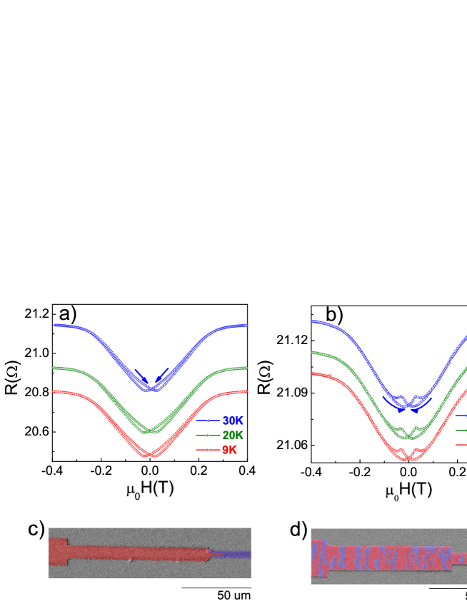
In Fig. 2, we present the magneto-transport behavior of the Ni/Nb planar structures at temperatures above the superconducting transition in presence of an in-plane applied magnetic field. These measurements are performed for a sample different from the one shown in Fig. 1(c). Panel 2(a) shows the response for magnetic field along the length while panel 2(b) shows the response in a field along the width of the stripe. Henceforth, keeping in mind that magnetic field is always applied in the plane of the substrate, throughout the text, we will refer to these two field configurations as longitudinal and transverse field, respectively. Intrinsic magneto-resistance of nickel was observed in longitudinal field (In Fig 2(a)), where the MR minima typically corresponds to the coercive field52 . This was found to be same irrespective of change in temperature value up to 30 K, due to very high Curie temperature of nickel. In transverse field configuration, MR peaks were observed with peak amplitude of 5.9 at the coercive field, as shown in Fig 2(b). The peak amplitude was found to be same for various temperatures up to 15 K. MR hysteresis was observed in both the configurations which is, however, an expected effect due to the magnetic hysteresis of the Ni layer. The difference is the additional peak in the MR hysteresis in the transverse field configuration when we have an order of magnitude more number of domain walls. The observed peak cannot be from anisotropic magnetoresistance (AMR) of Ni film in this case because (i) we have not observed the additional peak in the MR hysteresis of Ni thin films or in Ni/Nb bilayers in longitudinal or transverse field configurations, as shown in the supplementary Fig. S2 and (ii) the amplitude of DWMR peaks shown in Fig. 2(b) are temperature independent, which is unlike the behavior of AMR which is usually a temperature dependent quantity. We note that the peaks in MR, in transverse configuration, appear at field values corresponding to the minima in MR in longitudinal configuration, shown in panel 2(a). Usually, in a ferromagnetic film, the number of domain walls is maximum near the coercive field. Therefore, the origin of MR peaks in transverse configuration can be correlated to the number of domain walls. In order to verify this, we performed Kerr microscopy of nickel stripes of similar thickness in longitudinal and transverse configurations. As shown in panel 2(c), only two domain walls were observed in longitudinal configuration for fields applied near the coercive field. On the other hand, large number of domain walls were observed in transverse configuration near the coercive field as shown in panel 2(d). Therefore, in the transverse configuration, the DWMR contributions of a large number of domain walls add up to give the observed peaks in the MR curves. Whereas in the longitudinal configuration, due to the low number density of domain walls, no DWMR peaks were observed. The observation of a clear DWMR peak in the transverse field configuration ensures that, in this measurement geometry, an injected current passes through a large number of domain walls in the nickel stripe. Therefore, below the Tc of Nb in the gapped Ni/Nb bilayer stripes, it is very likely that a significant number of diffused singlet Cooper pairs will encounter a domain wall directly. Therefore, this is a suitable measurement configuration to look for any signatures of singlet to triplet conversion through domain walls upon decreasing the temperature below superconducting transition.
III.2 Magneto-transport below superconducting transition temperature on Nb
In Fig. 3, we present the magneto-transport behavior of the Ni/Nb planar structures at temperatures below the superconducting transition in the transverse configuration. Fig. 3(a) shows the magnetoresistance (MR) curve measured at 8 K which is very close to superconducting transition (Tc 8.3 K). Two distinct MR peaks were observed whose amplitudes were found to be more than 50 times higher than the normal state DWMR shown in Fig. 2(b). Since this measurement was done very close to the superconducting transition, the Nb layer is expected to respond to domain wall stray fields very sensitively. Therefore, the origin of MR peaks observed at this temperature is the usual suppression of superconductivity due to the out of plane component of domain walls present in nickel as observed in earlier reports44 ; Ekta . Since the overall domain wall stray field maximizes near the coercive field, the MR peaks, in this case appear near the coercive field. At lower temperatures, superconductivity is less sensitive to the out of plane stray field of nickel domain walls. Therefore, these peaks indicating suppression of superconductivity should diminish at lower temperatures. This is what we observe in the MR data measured at 7 K, as shown in Fig. 3(b). Moreover, we observe a DWMR peak with peak amplitude of 0.2 at 7 K as shown in the inset of Fig. 3(b).
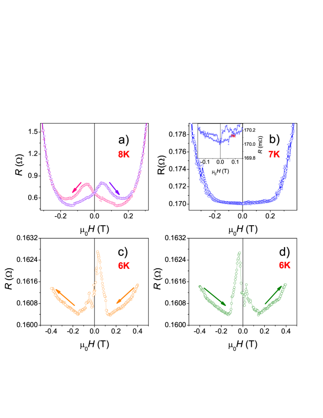
Fig. 3(c) and Fig. 3(d) show the MR measurements at a temperature of 6K with magnetic field swept in negative (+ve to -ve field) and positive (-ve to +ve field) directions, respectively. Since the effect of domain wall stray field was minimized below 7 K as shown in Fig.3(b), the DWMR effect was possible to observe. It can be seen in Fig. 3(c) that while decreasing the magnetic field from positive saturation the DWMR effect sets in as soon as domain formation starts, leading to increase in resistance. However, as the number of domain walls become significant, the resistance starts to decrease. Fig. 3(d) shows the same feature while ramping the field from negative saturation towards positive saturation. The spikes represent jumps in resistance due to abrupt re-configuration of vortices as reported earlier44 . The observed spikes cannot originate from the movement of the magnetic domain walls that reside in the FM layer under the action of the applied current. The reported values62 of current density which leads to domain wall motion is of the order of 108 A/cm2, which is many orders of magnitude higher compared to the current densities used in this case (104 A/cm2). Therefore, the possibility of magnetic domain wall motion is excluded in the present work. We observe that the DWMR at 6 K is more compared to that at 7 K. Earlier report on Nb/Garnet bilayer has shown that superconductivity shrinks the domains49 . Therefore, the increase in DWMR below 7 K may be due to an increased number of domain walls, as reported earlier49 . However, the unconventional drop in resistance can not be explained due to change in domain structure with temperature. The field dependent decrease in resistance can not be explained in terms of Nb-Ni proximity effect, because, it should be present at all field values. By studying the conductance-voltage characteristics, one can study the proximity effect at the interface of S-F hybrids60 ; 61 , which is not the purpose of the present work. Rather, the purpose of this work is to look at the changes in DWMR due to a direct proximity of the domain walls with the Cooper pairs, which is possible to measure via magneto-transport measurements. Here we note that unlike planar Josephson junctions, the large ferromagnetic gap of 3 m, in this case, forbids any direct coupling between the superconducting electrodes at the gap.
IV Discussion
In order to understand the suppressed DWMR effect in certain field range, in Fig. 4, we schematically show the different resistances seen by the current at temperatures above and below the superconducting transition. For temperatures above the superconducting transition, both Nb and Ni layers are normal metals, and they carry the total current in parallel according to their resistance values. A current going through the Ni layer encounters the domains and domain walls of nickel. Therefore, the effective resistance seen by the current in Ni layer consists of resistance of domains and domain walls .

At temperatures below the superconducting transition the resistance, , of the niobium electrodes become zero. The singlet Cooper pairs, which diffuse directly into the domain walls may convert into triplet pairs7 ; 34 ; 35 . The spin-diffusion length of Ni56 (212 nm) limits the decay length of triplet Cooper pairs beyond 23 nm, as predicted theoretically57 . Due to the long-range nature, the triplet Cooper pairs may reduce the effective resistance observed in Fig. 3(c) and 3(d) by reducing the domain resistance RD. The comparison of supplementary Fig. S3(a) and Fig. S3(b) shows that number of domain walls increases as one decreases the field from saturation and approaches the coercive field. We believe that increased number of domain walls increases the chances of direct Copper pair injection into the domain walls leading to an increase in singlet-triplet conversion and hence a decrease in resistance as the number of domains become significant. We must, however, discuss a few other possible scenarios which may lead to such anomalous decrease in magnetoresistance. In an earlier report 46 on Nb/BaFe12O19 bilayers the authors have ascribed sharp dips in MR to the onset of domain and domain wall superconductivity. However, we must point out that these measurements were done close to the transition temperature where domain and domain wall stray field can have a large effect. Therefore, this possibility can be excluded in our case because, our data (Fig.3) shows that below 7 K the stray field of domain walls no longer has any effect on the MR. Another possible effect that may cause an apparent decrease in magneto-resistance in hybrid S-F systems is the vortex locking effects 53 . In order to rule out this possibility we have measured the DWMR in the superconducting state with varying bias current. With increasing bias current, the Lorentz force on any possible vortices in the Nb layer would increase. Therefore, if vortex locking would have been the cause of the observed resistance drop in the DWMR peaks (Fig.3(c)), the corresponding field values would have been different at all bias currents. However, we find that the decrease in DWMR starts around the same field value for all bias currents (shown in the Supplementary Fig. S4). This observation indicates that the decrease in DWMR is connected to the magnetization dynamics of the Ni layer which remains unaffected by the bias current.
V Conclusion
In conclusion, we have studied DWMR for temperatures above and below the superconducting transition in a Ni/Nb planar structure. In the Ni/Nb bilayer stripe geometry, by carving a gap in the Nb layer, we are able to measure the DWMR of the Ni layer below Tc. In the conventional S-F bilayer geometries, used in the earlier reports, current is predominantly confined to the superconducting layers and the intrinsic DWMR property would not be possible to measure. We observed unconventional drop in DWMR of Ni layer at temperatures below the superconducting transition of Nb layer, which was not present in the normal state of the Nb layer. We believe that our measurement geometry allowed for direct injection of singlet Cooper pairs into the domain walls which resulted in singlet-triplet conversion leading to a decrease in the domain resistance. Since this process is dependent on the number of domain walls, the effect was apparent in the magnetic field range where number of domain walls maximized. We have excluded other possibilities leading to the observation of similar drop in MR, such as domain and domain wall superconductivity and vortex locking-unlocking effects. Although the triplet super-current generated by domain walls is not directly accessible, our experiment provides a possible indirect signature of the theoretically predicted singlet-triplet conversion effect of domain walls. This experiment may motivate measurement of planar Josephson junctions with a magnetic gap which accommodates a single pinned domain wall which would be useful for the field of superconducting spintronics.
VI Acknowledgements
KS acknowledge the funding from National Institute of Science Education and Research(NISER), DST-Nanomission (SR/NM/NS-1183/2013) and DST SERB (EMR/2016/005518) of Govt. of India.
References
- (1) A. I. Buzdin, Rev. Mod. Phys. 77, 935 (2005).
- (2) J. Linder, and J. W. A. Robinson, Nat. Phys. 11, 307–315 (2015).
- (3) M. Eschrig, Rep. Prog. Phys. 78, 104501 (2015).
- (4) F. S. Bergeret, A. F. Volkov, and K. B. Efetov, Phys. Rev. Lett. 86, 4096 (2001).
- (5) R. S. Keizer, S. T. B. Goennenwein, T. M. Klapwijk, G. X. Miao, G. Xiao, and A. Gupta, Nature 439, 825–827 (2006).
- (6) I. Sosnin, H. Cho, V. T. Petrashov, and A. F. Volkov, Phys. Rev. Lett. 96, 157002 (2006).
- (7) J. W. A. Robinson, J. D. S. Witt, and M. G. Blamire, Science 329, 59–61 (2010).
- (8) T. S. Khaire, M. A. Khasawneh, W. P. Pratt, and N. O. Birge, Phys. Rev. Lett. 104, 137002 (2010).
- (9) C. Klose, T. S. Khaire, Y. Wang, W. P. Pratt, Jr., N. O. Birge, B. J. McMorran, T. P. Ginley, J. A. Borchers, B. J. Kirby, B. B. Maranville, and J. Unguris, Phys. Rev. Lett. 108, 127002 (2012).
- (10) I. Eremin, F. S. Nogueira, and R-J. Tarento, Phys. Rev. B 73, 054507 (2006).
- (11) L. Trifunovic, Z. Popovic, and Z. Radovic, Phys. Rev. B 84, 064511 (2011).
- (12) A. G. Malśhukov, and A. Brataas, Phys. Rev. B 86, 094517 (2012).
- (13) M. Eschrig, and T. Löfwander, Nat. Phys. 4, 138143 (2008).
- (14) Y. Kalcheim, T. Kirzhner, G. Koren,and O. Millo, Phys. Rev. B 83, 064510 (2011).
- (15) C. Visani, et al. Nat. Phys. 8, 539 (2012).
- (16) P. V. Leksin, N. N. Garif’yanov, I. A. Garifullin, Y. V. Fominov, J. Schumann, Y. Krupskaya, V. Kataev, O. G. Schmidt, and B. Büchner, Phys. Rev. Lett. 109, 057005 (2012).
- (17) J. W. A. Robinson, F. Chiodi, G. B. Halász, M. Egilmez, and M. G. Blamire, Sci. Rep. 2, 1-6 (2012).
- (18) Y. V. Fominov, A. F. Volkov, and K. B. Efetov, Phys. Rev. B 75, 104509 (2007).
- (19) D. Fritsch, and J. F. Annett, Supercond. Sci. Technol. 28, 085015 (2015).
- (20) J. Ieda, S. Takahashi, M. Ichimura, H. Imamura and S. Maekawa, J. Magn. Magn. Mater. 310, 2058 (2007).
- (21) J. W. A. Robinson, S. Piano, G. Burnell, C. Bell, M. G. Blamire, Phys. Rev. B 76, 094522 (2007).
- (22) C. T. Hsieh, J. Q. Liu, and J. T. Lue, Appl. Surf. Sci. 252, 1899 (2005).
- (23) J. Silcox, Phil. Mag. 8, 7 (1963).
- (24) P. C.-Zimansky, Z. Jiang, and V. Chandrasekhar, Charge imbalance, New J. Phys. 9, 116 (2007).
- (25) K. Y. Arutyunov, S. A. Chernyaev, T. Karabassov, D. S. Lvov, V. S. Stolyarov and A. S. Vasenko, J. Phys.: Condens. Matter 30, 343001 (2018).
- (26) R. T. McGuire, and R. I. Potter, IEEE Trans. Magn. 11, 1018 (1975).
- (27) E. J. Patiño, C. Bell, and M. G. Blamire, Eur. Phys. J. B 68, 73-77 (2009).
- (28) E. Bhatia, Z. H. Barber, I. J. Maasilta, and K. Senapati, AIP Adv. 9, 045107 (2019).
- (29) M. Kläui, C. A. F. Vaz, J. A. C. Bland, W. Wemsdorfer, G. Faini, E. Cambril, L. J. Heyderman, F. Nolting and U. Rüdiger, Phys. Rev. Lett. 94 106601 (2005).
- (30) V. V. Vlasov, A. I. Buzdin, A. Melnikov, U. Welp, D. Rosenmann, L. Uspenskay, V. Fratello, and W. Kwok, Phys. Rev. B 85, 064505 (2012).
- (31) P. Charlat, H. Courtois, Ph. Gandit, D. Mailly, A. F. Volkov, and B. Pannetier, Phys. Rev. Lett. 77, 4950 (1996).
- (32) M. Giroud, H. Courtois, K. Hasselbach, D. Mailly, and B. Pannetier, Phys. Rev. B 58, R11872 (1998).
- (33) C. E. Moreau, I. C. Moraru, N. O. Birge, and W. P. Pratt, Appl. Phys. Lett. 90, 012101 (2007).
- (34) C. Cirillo, S. Voltan, E. A. Ilyina, J. M. Hernandez, A. Garcia-Santiago, J. Aarts, and C. Attanasio, New J. Phys. 19, 023037 (2017).
- (35) Z. Yang, M. Lange, A. Volodin, R. Szymczak, and V. V. Moshchalkov, Nat. Mater. 3, 793 (2004).
- (36) A. Yu. Aladyshkin, A. V. Silhanek, W. Gillijns and V. V. Moshchalkov, Supercond. Sci. Technol, 22, 053001 (2009).