Non-equilibrium Green’s function predictions of band tails and band gap narrowing in III-V semiconductors and nanodevices
Abstract
High-doping induced Urbach tails and band gap narrowing play a significant role in determining the performance of tunneling devices and optoelectronic devices such as tunnel field-effect transistors (TFETs), Esaki diodes and light-emitting diodes. In this work, Urbach tails and band gap narrowing values are calculated explicitly for GaAs, InAs, GaSb and GaN as well as ultra-thin bodies and nanowires of the same. Electrons are solved in the non-equilibrium Green’s function method in multi-band atomistic tight binding. Scattering on polar optical phonons and charged impurities is solved in the self-consistent Born approximation. The corresponding nonlocal scattering self-energies as well as their numerically efficient formulations are introduced for ultra-thin bodies and nanowires. Predicted Urbach band tails and conduction band gap narrowing agree well with experimental literature for a range of temperatures and doping concentrations. Polynomial fits of the Urbach tail and band gap narrowing as a function of doping are tabulated for quick reference.
I Introduction
The need for ultra-low power applications, efficient lighting and renewable energy sources have resulted in the development of novel devices such as the tunnel field-effect transistors (TFETs) Lind et al. (2015); Avci et al. (2015); Seabaugh and Zhang (2010), GaN/InGaN light-emitting diodes (LEDs) Geng et al. (2018); Laubsch et al. (2010); Guo et al. (2010) and high-performance solar cells Krogstrup et al. (2013); Bailey et al. (2011); Wallentin et al. (2013). Carrier transport and sub-60 mV subthreshold slope (SS) performance in TFETs, optical recombination and carrier generation in LEDs is highly dependent on a good description of conduction and valence band properties. Tailing of band edge states (known as Urbach tails/band tails) and band gap narrowing can significantly alter the device behaviour. For instance, the switching behaviour of TFETs is drastically affected by such band tailing Agarwal and Yablonovitch (2014); Bizindavyi et al. (2018). Exponentially decaying band tail states (below the conduction band and above the valence band) are known to fundamentally limit the lowest achievable SS in TFETs Lu and Seabaugh (2014); Agarwal and Yablonovitch (2014). On the other hand, band gap narrowing is known to alter the optical frequency at which recombination and carrier generation occurs in LEDs and solar cells. It also shifts the turn-on and threshold voltage of optical devices and the tunneling current in TFETs Geng et al. (2018); Oehme et al. (2013).
Band tailing and band gap narrowing effects are mainly attributed to the interaction of electrons and holes with phonons, randomly distributed dopant impurity atoms and native lattice disorders and defects. They exhibit a strong dependence on temperature and doping concentration. Halperin and Lax (1966, 1967); John et al. (1986); Jain and Roulston (1991) Though the effect has been studied for quite some time, actual values for specific materials are based either on heuristic models or parameters that are directly extracted from experimental observations. Halperin and Lax (1966, 1967); Jain and Roulston (1991); Zhang et al. (2016); Bizindavyi et al. (2018) This situation is inconvenient, since the validity of the heuristic expressions is limited by the doping range and underlying assumptions on the band dispersion. In addition, band gaps and tailing of confined devices such as ultra-thin body and nanowires are notoriously hard to predict without the presence of available experimental data.
In this work, band-tailing and band gap narrowing are predicted with scattering self-energies in the framework of the non-equilibrium Green’s function (NEGF) method. The predicted values depend only on material dependent parameters. The NEGF method is among the most detailed quantum transport methods for electronic, thermal and optoelectronic effects in a variety of nanodevices Datta (2000); Lake et al. (1997); Markussen et al. (2009); Lee and Wacker (2002); Steiger (2009); Kubis et al. (2009). It has been applied in modeling transistors Luisier and Klimeck (2009); Afzalian et al. (2018); Ameen et al. (2017), resonant-tunneling devices Bowen et al. (1997), metal-semiconductor contacts Sarangapani et al. (2018); Hegde and Chris Bowen (2014), phonon transport across interfaces Miao et al. (2016), GaN/InGaN light-emitting diodes Geng et al. (2018) with quantitative agreements with experimental data. In this work, incoherent scattering is modeled through scattering self-energies within the self-consistent Born approximation (SCBA). Lake et al. (1997) Amongst the scattering mechanisms present in doped III-V semiconductors, polar optical phonons (POP) and charged impurity scattering mechanisms are the dominant mechanisms Riddoch and Ridley (1983); Fischetti and Laux (1988). Both scattering mechanisms are considered including electrostatic screening effects. The scattering self-energies for both scattering mechanisms are derived for ultra-thin bodies and nanowires and then verified against Fermi’s golden rule. Urbach tails and band gap narrowing parameters are extracted from the NEGF predicted density of states (DoS) for GaAs, InAs, GaSb and GaN and respective nanodevices. Simulated results are benchmarked against experimental data. A simple analytical formula for Urbach tail and band gap narrowing in ultra-thin bodies and nanowire devices is fit against the NEGF predictions and respective parameters are provided as guideline values.
II Simulation approach
II.1 Device representation
All NEGF simulations in this work have been performed with the multi-purpose nanodevice simulation tool NEMO5. Steiger et al. (2011) Bulk, ultra-thin body and nanowire devices considered in this work are all modeled in atomic resolution with the atoms in their native lattice. GaAs, InAs and GaSb are considered in the conventional zincblende cystal structure and GaN in the wurtzite structure. A 10-band sp3d5s* tight-binding Hamiltonian is used to describe conduction and valence bands. Klimeck et al. (2000); Jancu et al. (2002) Both POP and charged impurity scattering mechanisms are long-ranged and the extent of non-locality is determined by the electrostatic screening length. For all the discussions in the subsequent sections, the respective device is assumed to be in equilibrium with the density corresponding to the doping concentration. Self-energies derived are solved self-consistently with the corresponding Green’s function following the self-consistent Born approximation scheme. The convergence is achieved once maximum relative particle current variation of is given throughout the device. The retarded () and lesser than () Green’s functions are solved with
| (1) |
where and are the retarded and lesser scattering self-energies for polar optical phonon scattering and and are the retarded and lesser scattering self-energies for charged impurity scattering.
II.2 Scattering self-energy formulas
Charged impurity scattering is modeled assuming homogeneously distributed impurity atoms. In this work, Brooks-Herring impurity scattering Brooks (1951) is employed due to the considered doping concentration ranging from up to ). The screened impurity scattering potential is given by
| (2) |
where is the number of electrons in a single dopant atom (taken to be 1 in this work) and is the screening length. The positive elementary charge is given by and is the vaccuum permitivity. Electrostatic screening of conduction band electrons is calculated within the Lindhard formalism Lindhard (1954) where the screening length is represented as
| (3) |
where is the electronic distribution function and the momentum integral runs over the first Brillouin zone. For this and all following expressions, three dimensional vectors are denoted with a and two dimensional vectors are boldfaced.
The Fröhlich coupling is considered for the electron-phonon interaction potential Fröhlich (1952)
| (4) |
The static and dynamic dielectric constants are represented by and respectively. The phonon frequency and momentum are denoted with and , respectively. The LO phonons are assumed as plane waves in all directions for bulk, UTBs and nanowires. The longitudinal-optical (LO) phonon frequency is assumed to be momentum independent and to agree with its value at the point. Phonon frequencies and dielectric constants used for GaAs, InAs, GaSb and GaN are listed in Table 1.
| GaN | GaAs | GaSb | InAs | |
| LO phonon frequency () | 92 meV | 36 meV | 30 meV | 30 meV |
| Static dielectric constant () | 10.4 | 12.95 | 15.69 | 12.3 |
| Infinite freq. dielectric constant () | 5.47 | 10.9 | 14.4 | 11.6 |
Electron scattering on charged impurities and polar optical phonons is non-local which yields significant numerical load. To limit the numerical burden, the integrals in the scattering self-energies are solved analytically as far as possible. Therefore, the self-energies are formulated separately for each confinement setting (ultra-thin body and nanowires). For completeness, the formulas for three dimensional, unconfined (bulk) systems are listed here as well. All scattering self-energy formulas below are given in position representation for nanowires, in position space and one dimensional momentum space for ultra-thin bodies and in position and two dimensional momentum space for bulk systems, respectively. The position representation translates directly into the atomistic tight binding, since all atoms have different coordinates. Interorbital transitions are only included on the same atom, i.e. when the two position coordinates of the scattering self-energy agree. On the same atom, all interorbital transitions are considered equally likely. Nonlocal scattering between different atoms is limited to same orbital types only to reduce the peak memory usage and the time to solution. To correct this underestimation of nonlocal scattering, the scattering self-energies are multiplied with a compensation factor that is deduced from Fermi’s golden rule as detailed in Sec. II.5.
The general expression for the retarded and lesser scattering self-energy of electrons scattering on homogeneously distributed charged impurities read Kubis et al. (2009)
| (5) |
where the momentum integral runs over the first Brillouin zone. Deriving expressions for different levels of periodicity, we have the following expressions for bulk, ultra-thin body and nanowires. Impurity scattering self-energies in 3D periodic systems (bulk) can be expressed as Kubis et al. (2009); Lake et al. (1997)
| (6) |
Charged impurity scattering self-energies for UTB devices read
| (7) |
where
| (8) |
where is the Bessel-K function of order 1. Finally, charged impurity scattering self-energies for nanowires can be expressed as
| (9) |
All analytical results for the scattering kernels above assume momentum integrations run from rather than over the first Brillouin zone only. Since the scattering potentials decay sharply with increasing momentum, this approximation does not affect the overall result. Kubis et al. (2009)
The general expression for the lesser scattering self-energy of electrons scattering with phonons reads Wacker (2002)
| (10) |
where is the number of phonons due to the Bose distribution evaluated for the LO phonon energy. The momentum integral in Eq. 10 runs over the first Brillouin zone. Starting with this expression and solving for each degree of periodicity, we get
| (11) |
| (12) |
for bulk systems. This expression has been used extensively in modeling quantum cascade lasers Kubis et al. (2009) and LEDs Steiger (2009). The POP phonon scattering self-energies for UTB devices reads
| (13) |
| (14) |
where
| (15) |
is the Bessel-K function of order 1. Finally, POP scattering self-energies in nanowires can be written as
| (16) |
| (17) |
where
| (18) |
Similar to the charged impurity scattering self-energies derivation, the phonon momentum integration is assumed to run over . In the numerical implementation of the retarded self-energies for inelastic scattering on polar optical phonons, the principal value integrals are neglected due to their minimal contribution but rather high numerical load. Esposito et al. (2009)
II.3 Band tails and band gap narrowing
The Urbach band tail parameters () are extracted from the slope of the exponentially decaying density of states below the band edge
| (19) |
where is one LO phonon energy below the ballistic band edge and is an integer number of phonon energies below . The Green’s functions are evaluated at a position in the center of the device. To compensate for small numerical fluctuations of the band tail, Eq. 19 is solved for several ranging between 2 and 4 LO phonon energies below . The average of these values is then used for the actual result.
The real part of the retarded scattering self-energy provides an energy shift and the imaginary part provides a energy broadening of the electronic states. Band gap narrowing is determined by running two sets of simulations - the first simulation solves for only the imaginary part of the retarded self-energy and its real part is set to zero. In that case, the band edges agree with those of ballistic calculations. In the second NEGF calculation the full retarded self-energy is solved. Note that the retarded self-energies only then fulfills the Kramers-Krönig relation. The band edges of this second case are defined as those energies where the density of states amplitude agrees with the band edge density of state amplitude of the first case, i.e. of the NEGF solution with purely imaginary retarded self-energy. The band gap narrowing is assumed to equal the differences in the band edges of those two cases.
| (20) |
II.4 Scattering rates from retarded self-energies
Self-energies are verified by comparing their on-shell scattering rates against corresponding Fermi’s golden rule results. On-shell scattering rates are computed by performing a basis transformation on the imaginary part of the retarded self-energy from the Wigner coordinate () to the momentum space ( being the transport direction). In many-band tight-binding, for a given energy-momentum (E-k) tuple, multiple on-shell target momentum values can be available to Fourier transform . All their contributions need to be summed up for each respective E-k tuple. For ultra-thin bodies and nanowires, the self-energy is first transformed into the space spanned by the corresponding cross sectional modes . Then they are Fourier transformed to get both the inter and intra-mode scattering rates.
Following are the on-shell scattering rates as functions of retarded self-energies for bulk Wacker (2002), ultra-thin bodies and nanowires
| (21) |
| (22) |
| (23) |
| (24) |
where is the mode-space self-energy, is the eigenmode transformation matrix and is the lattice constant. Note that inelastic scattering in NEGF yields band tails in the band gap. Since those are not part of the linear response Fermi’s golden rule in the next section, all NEGF-based scattering rate results are truncated for energies in the band gap.
II.5 Scattering rates from Fermi’s golden rule
Due to the non-local nature of scattering, the Fermi’s golden rule formulas are separately derived for each degree of confinement similar to Ref. Goodnick and Lugli, 1988. Envelope wave functions of the form
| (25) |
for bulk,
| (26) |
for ultra-thin body, and
| (27) |
for nanowires are assumed. The scattering rate is solved with Fermi’s golden rule for the bulk case with
| (28) |
Here, is the transferred momentum during scattering. and are the electronic distribution functions for initial and final states. Scattering rates for ultra-thin body and nanowire are accordingly given with
| (29) |
| (30) |
where and are initial and final UTB and nanowire modes, respectively. The transition element for bulk, ultra-thin bodies and nanowires read
| (31) |
| (32) |
| (33) |
and
| (34) |
| (35) |
Inserting Eq. 2, the Fermi’s golden rule for electrons scattering on charged impurities in bulk results in
| (36) |
The Fermi’s golden rule for electrons in ultra-thin body mode scattering on charged impurities into mode reads
| (37) |
where
| (38) |
The form factor is given by
| (39) |
where
| (40) |
The total scattering rate that mode faces is a sum of all possible mode transitions
| (41) |
The Fermi’s golden rule for electrons in nanowire mode scattering on charged impurities into mode can be written as
| (42) |
Form factor is given by
| (43) |
where the integration area and
| (44) |
The total scattering rate of mode is a sum of all intermode transitions likewise Eqn. 56.
The Fermi’s golden rule for electrons scattering on polar optical phonons in bulk are expressed below with absorption and emission branches given separately.
Bulk - Absorption process
| (45) |
where the integration limits of are
| (46) |
Bulk - Emission process
| (47) |
where the integration limits of are
| (48) |
and represents the Heaviside step function.
Total scattering rate is the sum of emission and absorption processes and is given by
| (49) |
In a similar way, the absorption and emission contributions to the Fermi’s golden rule for electrons in the ultra-thin body mode scattering on polar optical phonons into mode can be expressed as
UTB - Absorption process
| (50) |
where
| (51) |
UTB - Emission process
| (52) |
where
| (53) |
Form factor is given by
| (54) |
where
| (55) |
The total scattering of electrons in the mode is the sum of absorption and emission processes
| (56) |
The rates for absorption and emission of polar optical phonons of electrons in the nanowire mode scattering into mode read
Nanowire - Absorption process
| (57) |
| (58) |
Nanowire - Emission process
| (59) |
| (60) |
Form factor is given by
| (61) |
where
| (62) |
Similar to the scattering rate formulas above the total scattering rate of electrons in the nanowire mode is the sum of absorption and emission into all possible modes .
II.6 Compensation factor for non-local scattering self-energies
It was shown in Sec. II.2 that the electron scattering on polar optical phonons and charged impurities are non-local. Accounting for that full nonlocality in atomistic NEGF is numerically very expensive. Neglect of nonlocal scattering underestimates scattering and orbital diagonal scattering for a given position violates selection rules Aeberhard (2019). In this work, the numerical implementation of the self-energies described above are limited to atom-blockdiagonals only, i.e. nonlocal effects are included only within the range of a single atom. Interorbital transitions are only allowed within the same atom. To correct this underestimation of scattering, a compensation factor is deduced from the Fermi’s golden rule results in Sec. II.5. The compensation factor is defined as the ratio of the Fermi’s golden rule form factors for the local approximation vs. the full non-local formula. The compensation factor for UTBs and nanowires can be represented as
| (63) |
and
| (64) |
For electrons scattering on charged impurities, the UTB and nanowire cases read
| (65) |
and
| (66) |
For electrons scattering on polar optical phonons, they read
| (67) |
and
| (68) |
The discretization of nonlocal scattering depends on the real space mesh size. Self-energy matrices that are diagonal in the real space representation cover nonlocal scattering only within the volume represented by each single mesh point, i.e. each single atom. Therefore, the compensation factors depend on the mesh spacing and vary with system dimensions. To accurately represent the zincblende lattices of this work, the mesh spacing is chosen to agree with the spacing between subsequent atomic planes in [100] direction (i.e. ). Accordingly, the integrals for the denominators of Eqs. (63) and (64) run over the atomic volume. Note that Fermi’s golden rule formulations in bulk systems do not contain real space information - in contrast to the NEGF self-energies. Thus, a formulation of Eqs. (63) and (64) for bulk is not possible. Nevertheless, 50 nm UTBs with 20 electronic modes can mimic bulk behavior sufficiently well. The compensation factors of 50 nm UTB cases are therefore used in this work as bulk compensation factors.
III Results and discussions
III.1 Scattering rate comparison with Fermi’s golden rule
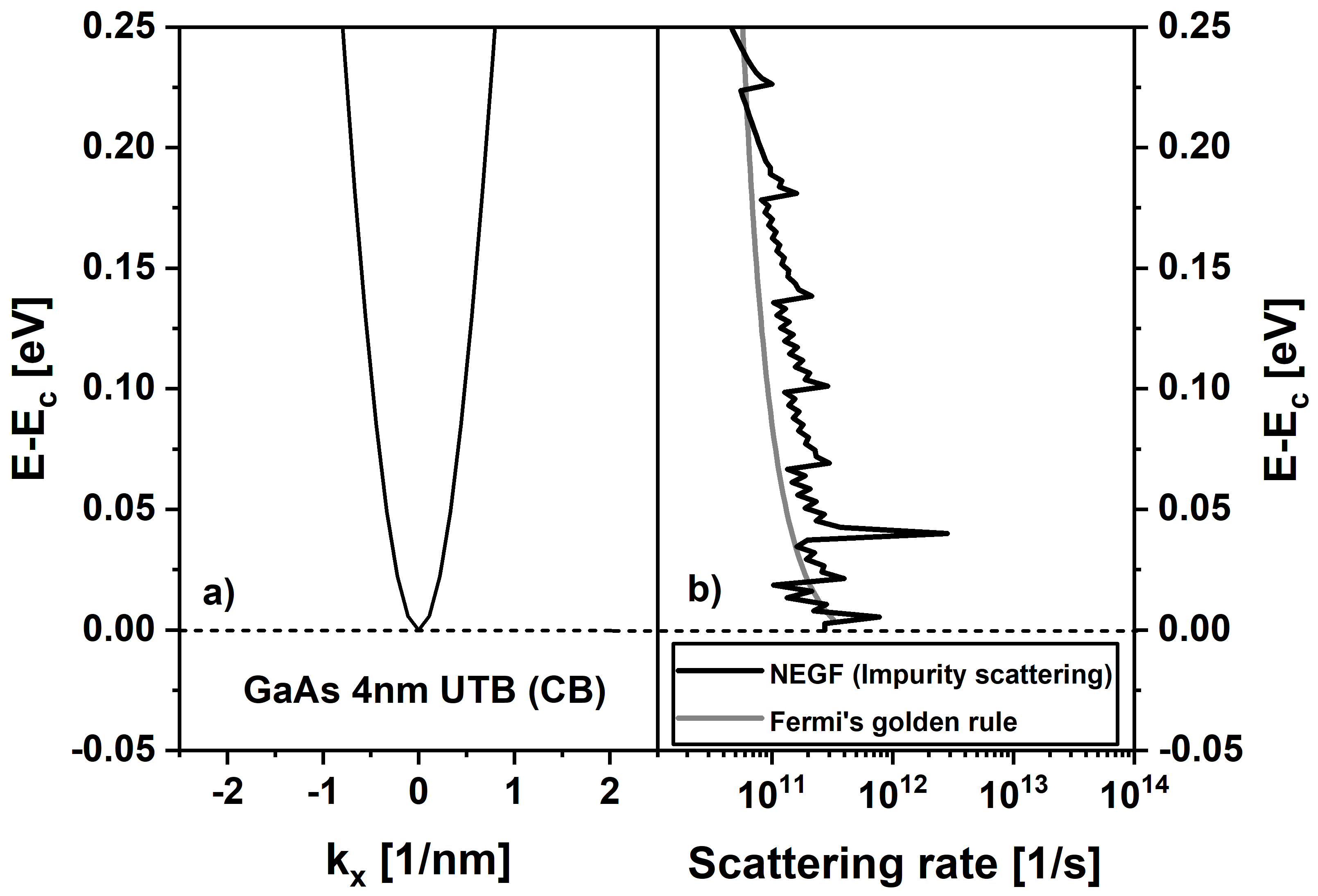
To verify the approximate treatment of nonlocal scattering self-energies of Sec. II.2, we benchmark the scattering rates of NEGF calculations against Fermi’s golden rule in bulk, UTB and nanowire equilibrium systems. The energy resolved scattering rate of electrons scattering on charged impurities follows the electronic density of states multiplied with the impurity scattering potential. The latter introduces a dependence of the rate, as can be seen in Fig. 1 for conduction band electrons in a 4nm GaAs ultra-thin body. The NEGF predicted scattering rate shows a good agreement with Fermi’s golden rule. Note that the spikes in the NEGF rate result from the finite numerical resolution of the transverse momentum space. Finer momentum meshes produce smoother NEGF scattering rates, but require significantly larger computational resources Datta (2005).
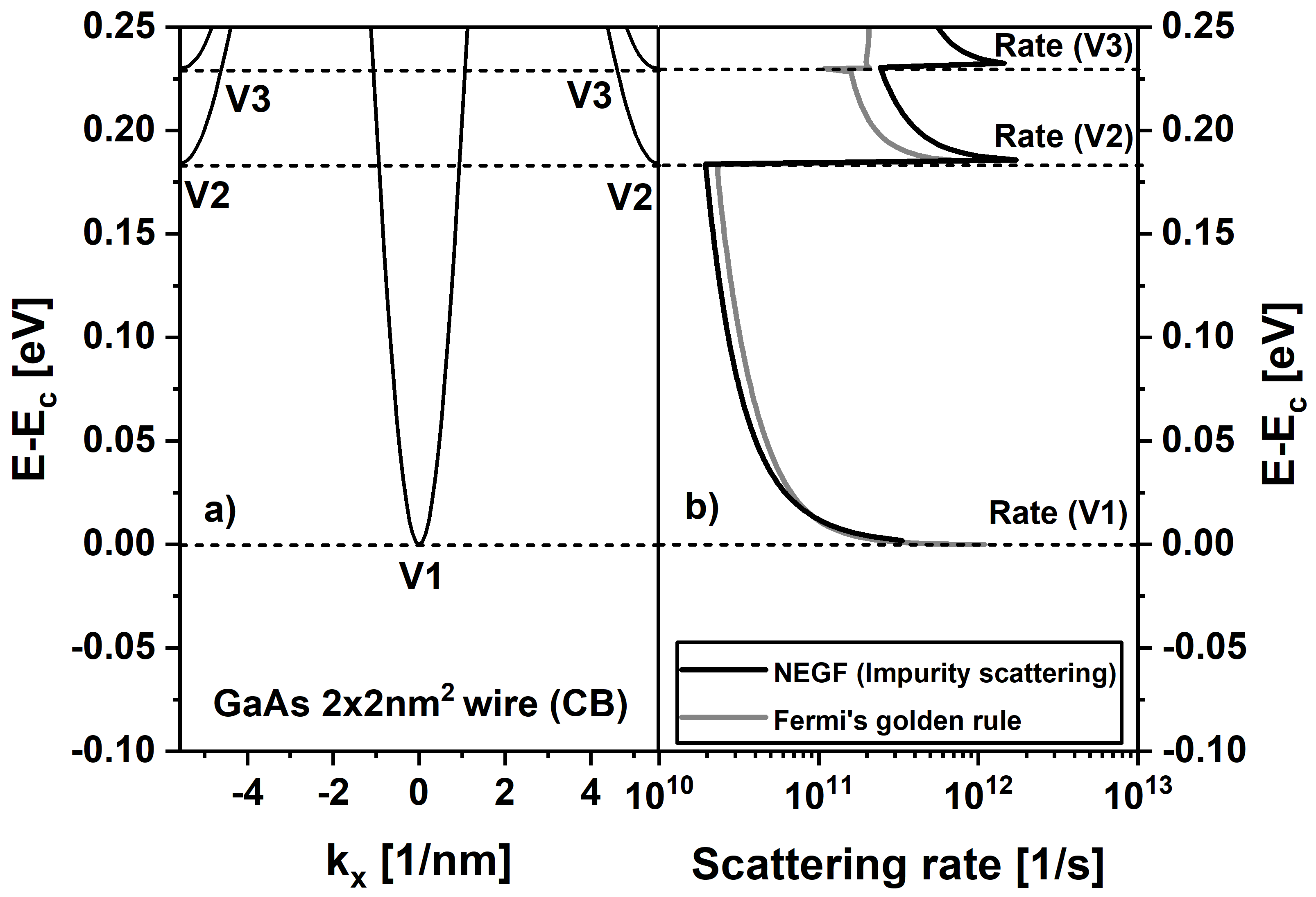
Similarly, NEGF results of nanowire electrons scattering on charge impurities show good agreement with Fermi’s golden rule (see Fig. 2). Short of a momentum degree of freedom and the related resolution challenges, the scattering rates smoothly follow the 1D density of states. The steps in the scattering rates coincide with valley energies and mark the onset of additional inter-valley and intra-valley scattering.
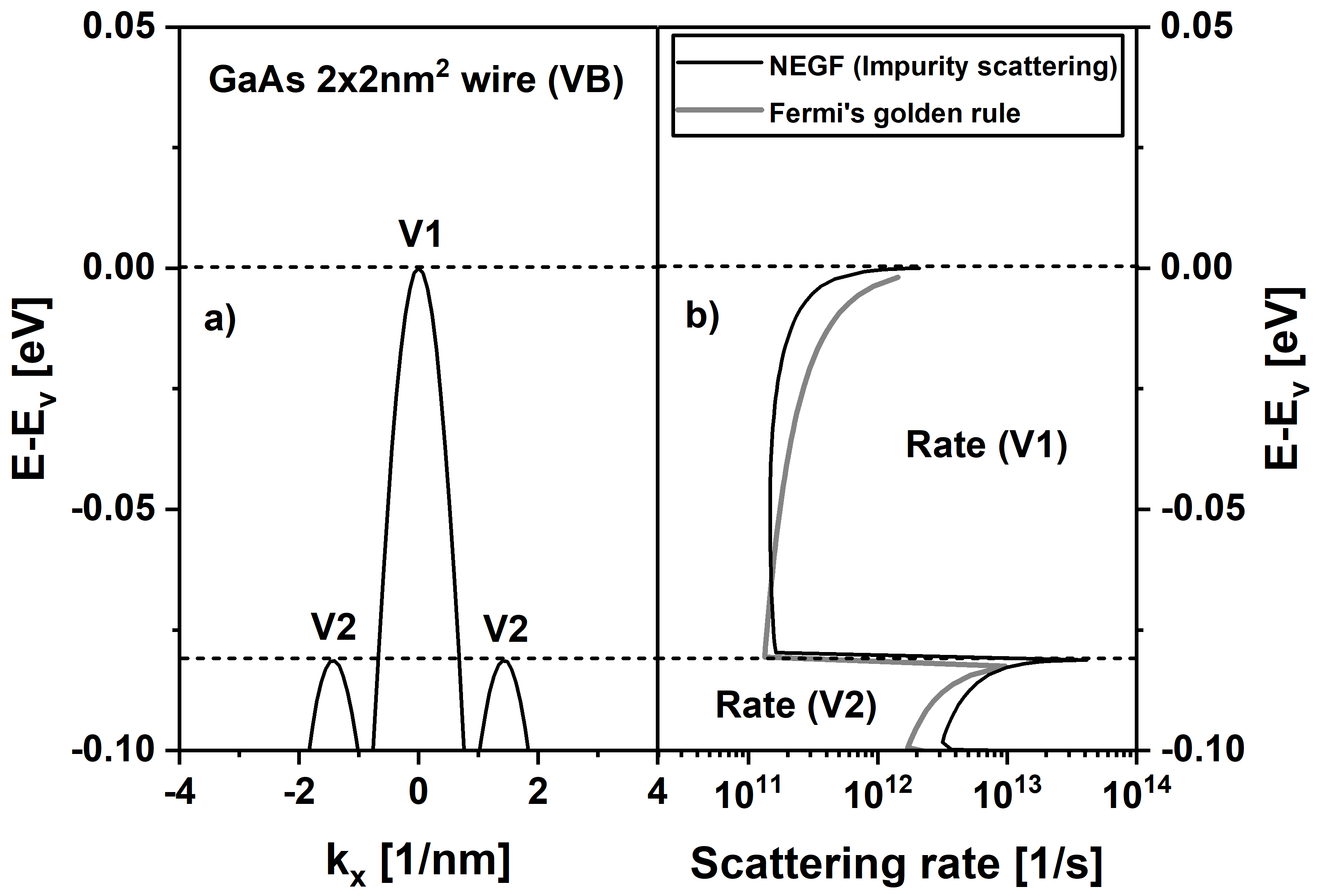
GaAs valence band states are mainly composed of p-orbitals, whereas electronic wavefunctions at the conduction band edge are mainly s-orbital type Tan et al. (2015). Therefore, inter-orbital scattering is expected to be more important in the valence band. Figure 3 compares the scattering rates of GaAs valence band electrons. The good agreement between the NEGF results and Fermi’s golden rule suggests the approximation of equal inter-orbital self-energy elements is appropriate. It is worth to mention that neglecting inter-orbital scattering on the same atom typically reduces the scattering rates by about . Remaining deviations of NEGF and Fermi’s golden rule results can be addressed to the effective mass dispersion assumed for the Fermi’s golden rule results in contrast to the multi-band atomistic treatment in NEGF. Note that the scattering rate at the valence band edge is smaller than the rate at the onset of the next valley (labeled V1 and V2 in Fig. 3, respectively) due to the ratio of the valley effective masses and their impact on scattering density of states.
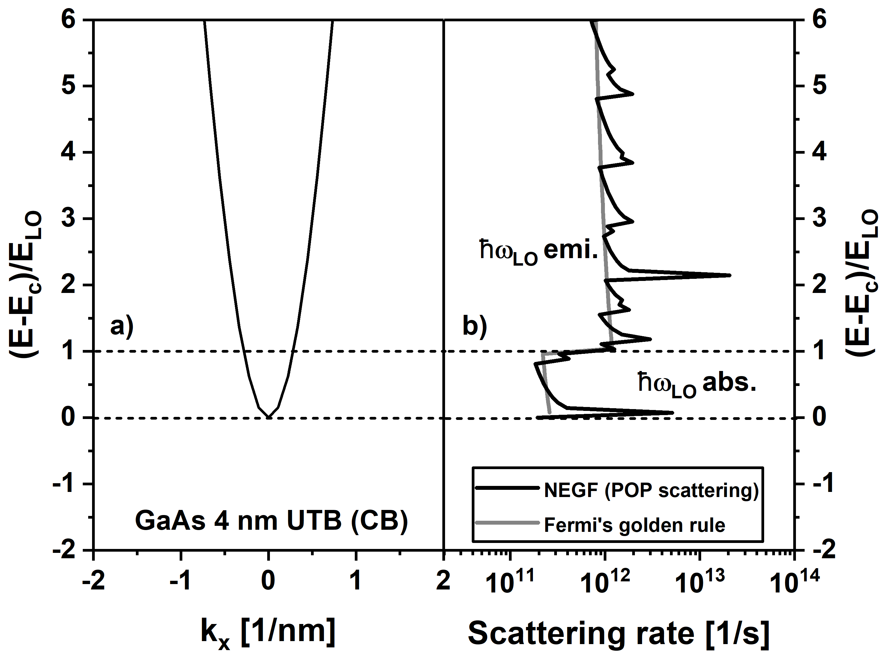
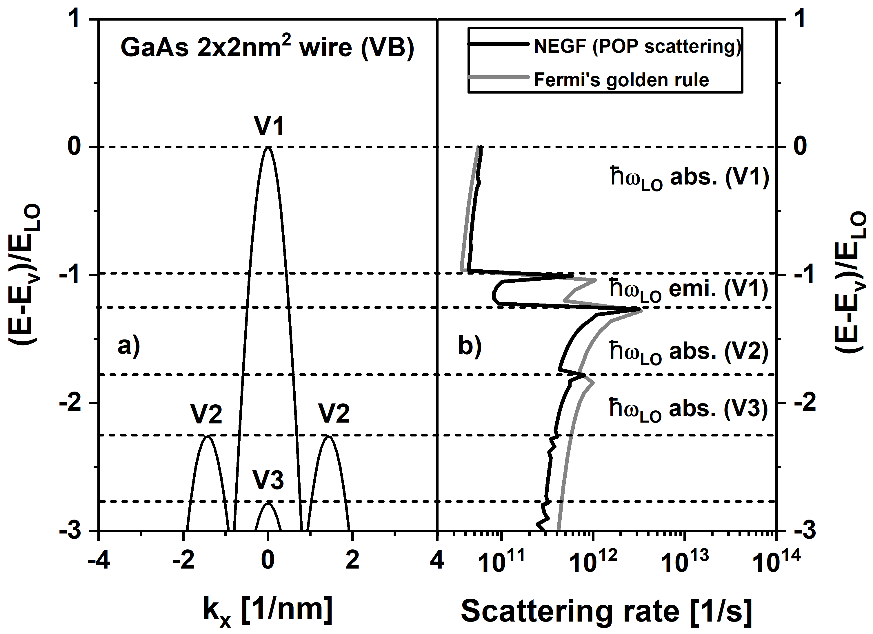
The rates for electron scattering on polar optical phonons predicted with NEGF and Fermi’s golden rule of GaAs UTB conduction band and nanowire conduction and valence bands are shown in Figs. 4, 5, and 6. NEGF scattering rates in UTBs (Fig. 4) exhibit spikes due to the numerical resolution of transverse momentum space similar to the impurity scattering in Fig. 1. All the results show steps when phonon emission and absorption processes at energy above or below the various band and valley edges step in.
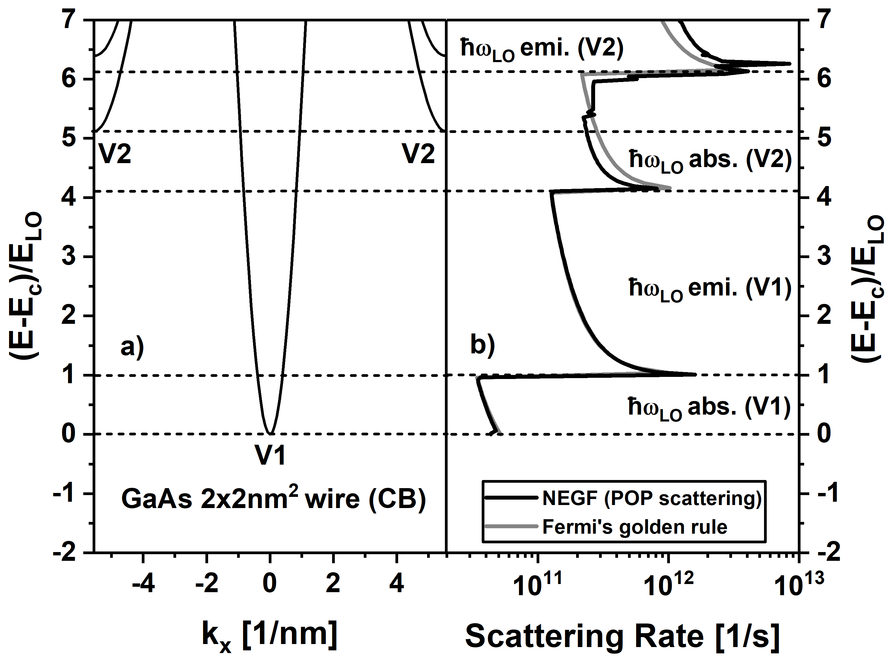
The scattering rates in Fig. 5 clearly shows absorption and emission processses for valleys V1 and V2. For energies near the conduction band edge, the rate includes phonon absorption and emission of electrons in valley V1 only. Electrons with energies of above the V1 edge can absorb LO phonons and scatter to valley V2 which results in an abrupt rate increase. Electrons in V2 with a total energy exceeding the V2 edge by one can emit LO phonons within the same valley. Thus, the scattering self-energies capture inter-valley and intra-valley scattering processes. Similar feature can be seen in Fig. 6 for electrons in the valence band.
III.2 Urbach tail predictions vs. temperature, doping and confinement
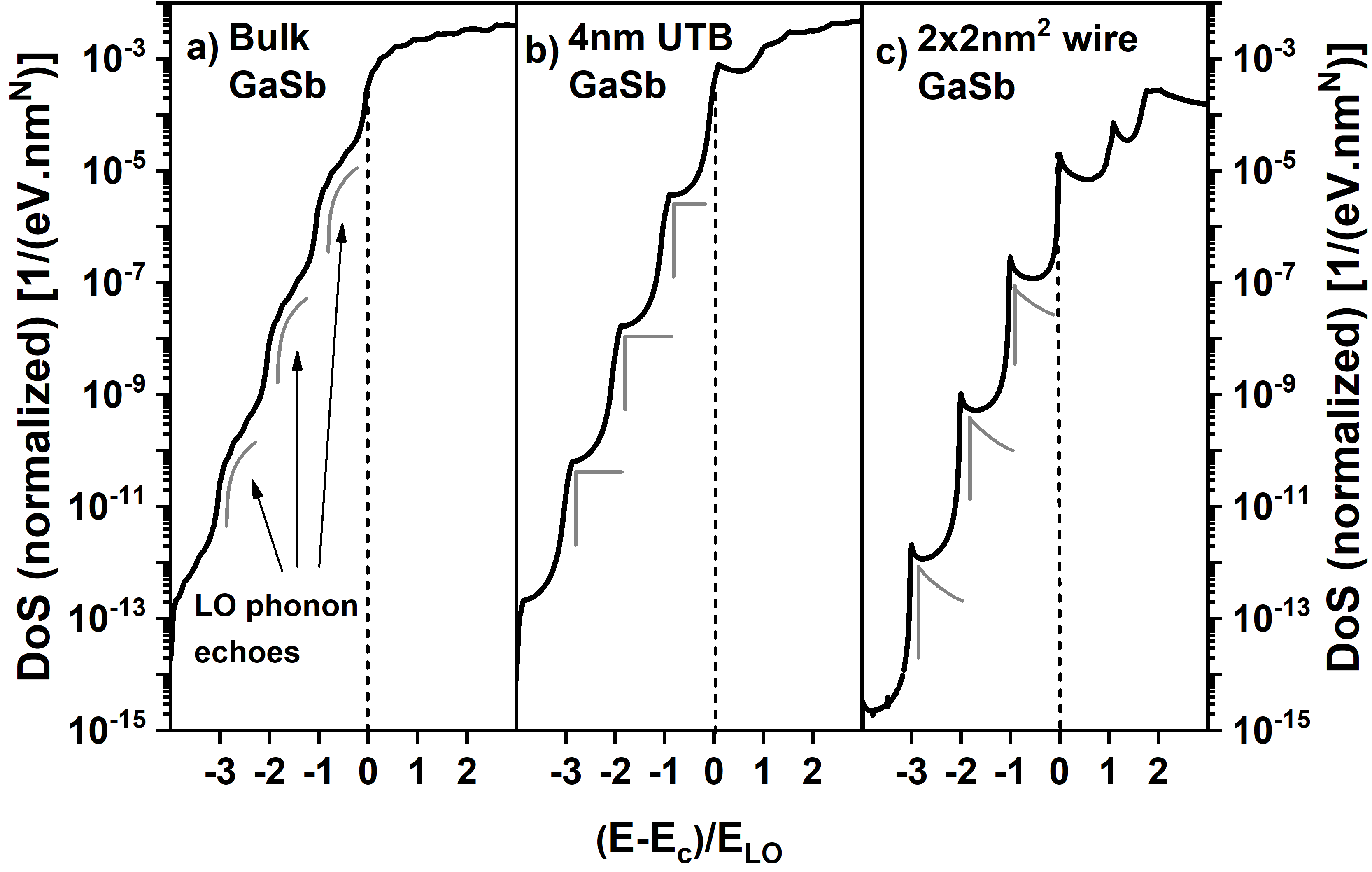
Urbach tails are an important aspect for optical experiments and the linewidth of absorption spectra Dow and Redfield (1972); Agarwal and Yablonovitch (2014); Khayer and Lake (2011). Figure 7 shows the density of states of electrons in GaSb bulk, in a GaSb ultra-thin body and in a GaSb nanowire when scattering on charged impurities and polar optical phonons. The electronic density of states in the presence of scattering on polar optical phonons and charged impurities differs from the ballistic case that drops sharply at the ballistic bandedge (marked with dotted line in Fig. 7). The considered scattering processes enhance the density of states below the bandedge into an exponential decaying band tail. The shape of band tails is determined by the nature of the density of states close to the bandedge and the formation of LO phonon echos Antonioli et al. (1981).
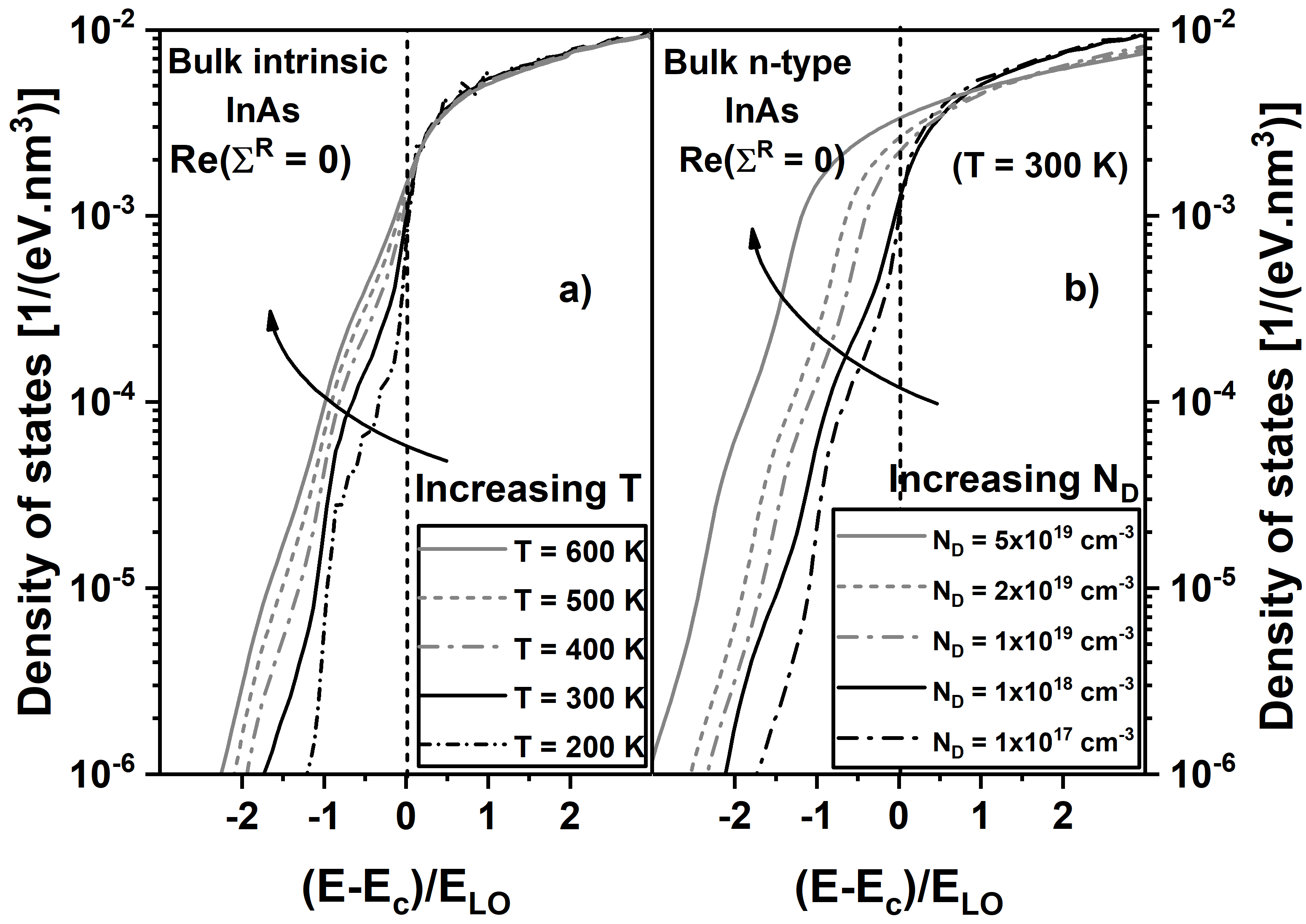
Figure 8 shows the variation of the conduction band tail with doping concentration and temperature. The phonon self-energies increase exponentially with temperature, which yields larger band tails (see Fig. 8). Impurity scattering is an elastic process and does not directly contribute to the band tail formation. However, once inelastic scattering on phonons creates a finite band tail, elastic scattering on charged impurities enhances the density of states at every energy in the band tail. Therefore, with increasing doping concentration, the band tail becomes larger and results in increasing Urbach parameters with doping.
With increasing doping and increasing temperature, phonon echoes are gradually washed out. This is due to increasing momentum randomization during scattering on impurities and polar optical phonons. Increasing temperatures enlarge the Lindhard screening length (see Eq. 3), which in turn supports larger differences of initial and final momentum in the exponents of the impurity and pop self-energies (see Eqs. (6), (7), (11) and (13)). In this way the electronic dispersion at the band edge and with it the LO phonon echos gets blurred with increasing temperatures.
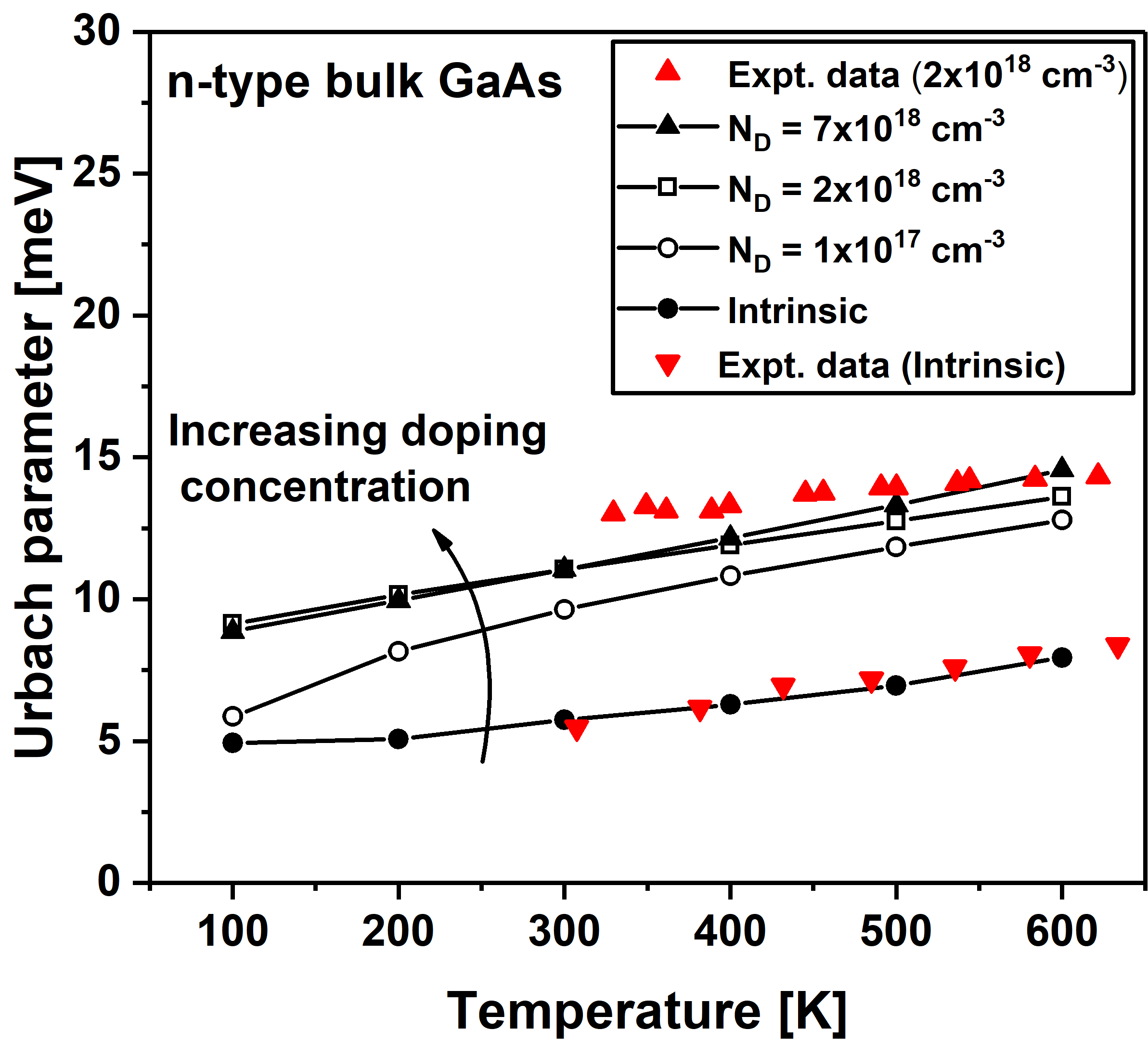
As detailed in section II.3, the Urbach parameter is a scalar parameter that characterizes band tails. Figure 9 shows the variation of the Urbach parameter in bulk GaAs as a function of temperature for different doping concentrations predicted with NEGF and compared against experimental data of Ref. Johnson and Tiedje, 1995. The NEGF results agree quantitatively with the experimental data for the intrinsic material over a large temperature range. The results agree well for the n-doped case. The deviations in the doped case likely originate from scattering on disorder effects and neutral impurity potentials that come along with doping, but are neglected in the NEGF calculations.
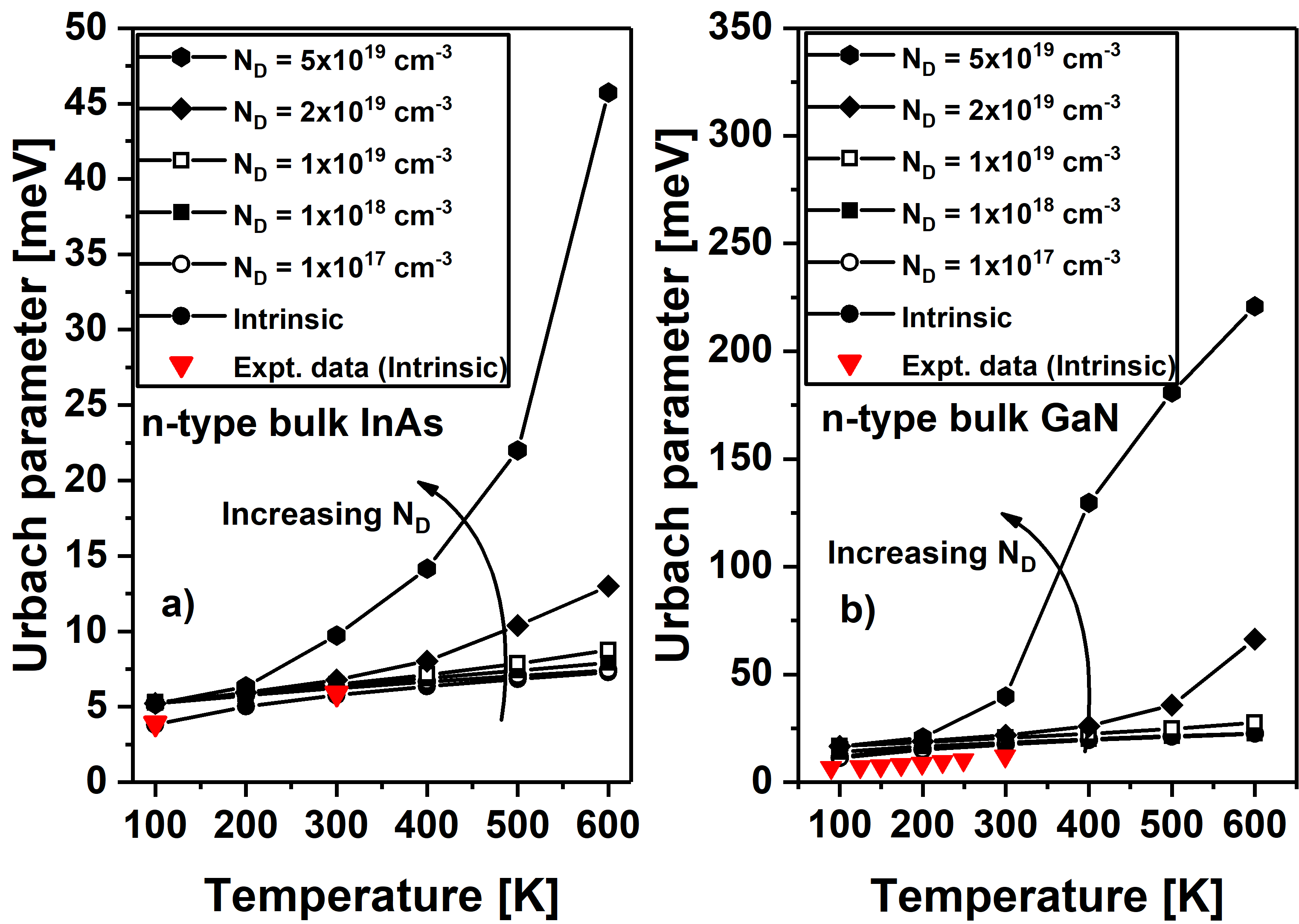
Figures 10 a) and b) show the Urbach parameter for InAs and GaN. Also here, the NEGF predictions agree well with the experimental data of Refs. Antonioli et al., 1981 and Chichibu et al., 1997, for InAs and GaN, respectively. The Urbach parameter value strongly depends on the strength of scattering potentials and available density of states near the band edge. The dielectric constants of GaN and the larger LO phonon energy of GaN ( meV) supports stronger LO phonon scattering in GaN than in InAs (phonon energy of meV). In addition, GaN has a conduction band effective mass () that is larger than the one of InAs () which enhances the density of states near its band edge. Consequently, Figs. 10 show larger Urbach parameters with a stronger temperature dependence in GaN.
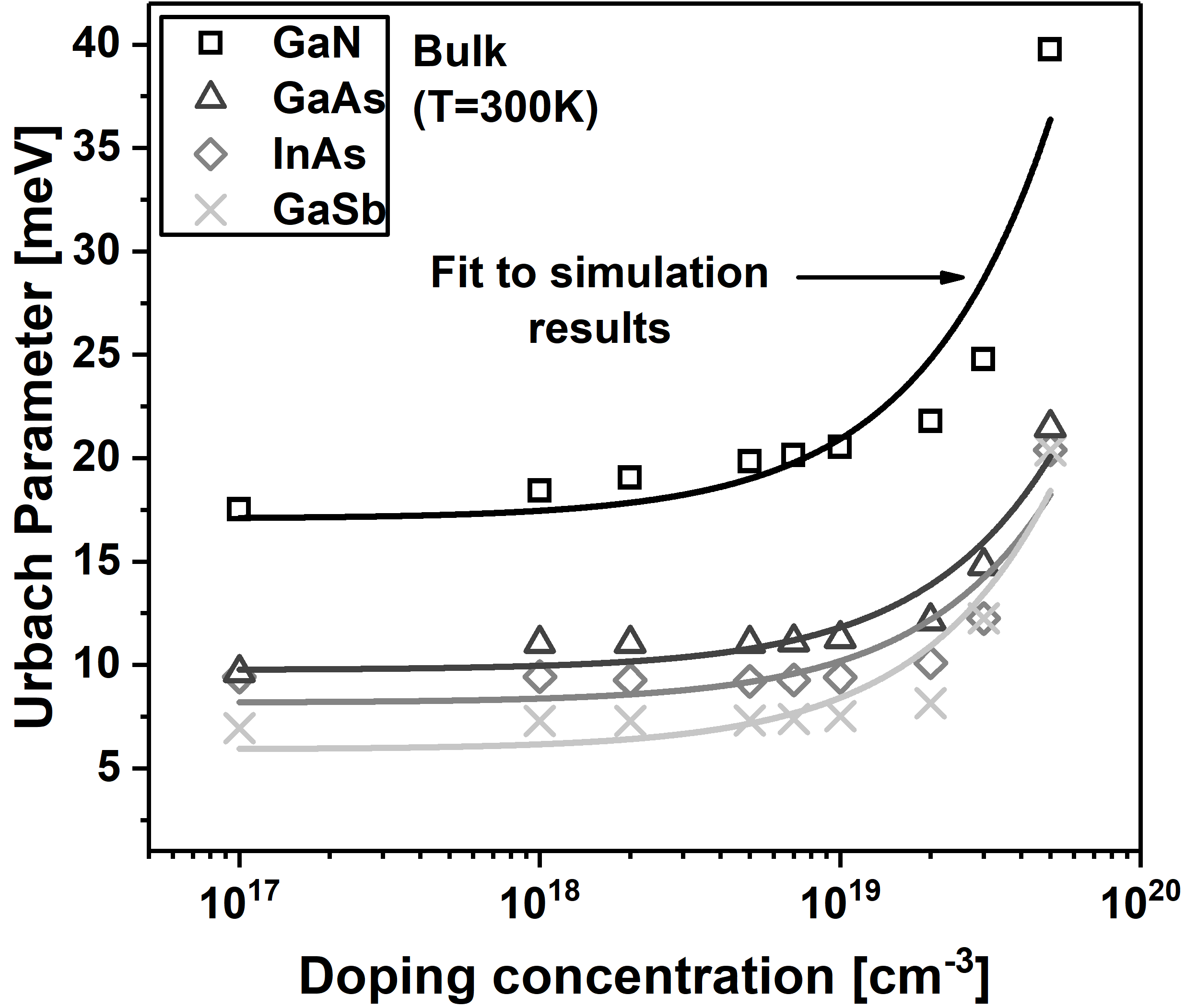
Figure 11 shows the simulated Urbach parameter of GaN, GaAs, InAs and GaN as a function of the doping concentration. The behavior of the Urbach parameter with increasing doping concentration can be fit to (lines in Fig. 11). We follow e.g. Refs. Jain et al., 1990; Jain and Roulston, 1991; Lee et al., 1995 in using a polynomial fit function for the Urbach parameters and band gap narrowing. The fitted parameters are given in Table 2.
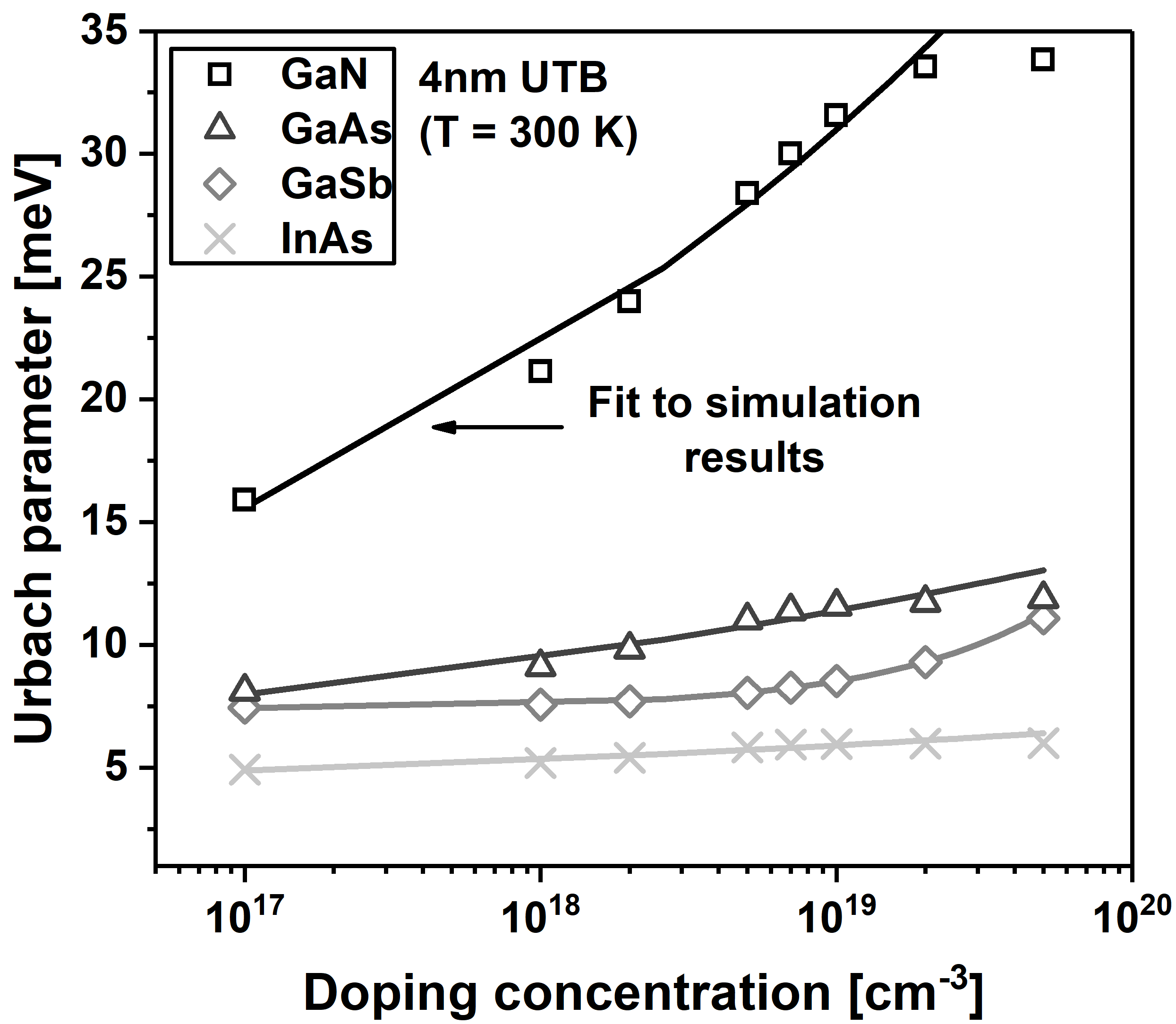
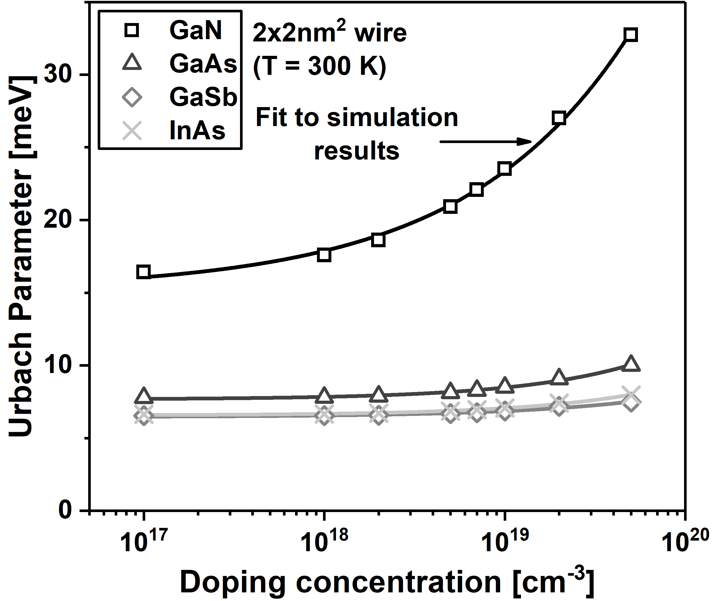
A similar dependence of the Urbach parameter on the doping concentration is found in Figs. 12 and 13 for UTBs and nanowires, respectively. The fitted curves in Figs. 12 and 13 capture the simulated results well. The corresponding fitting parameters are given in Table 2. The doping dependence of the Urbach parameter differs significantly for bulk, UTB and nanowires. For instance, it is approximately linear in the case of bulk and sub-linear with for nanowires. That behavior arises from three contributions - explicit doping dependence in impurity scattering potentials, implicit doping dependence through electrostatic screening and screening dependent non-local scattering ranges as can be seen from Eqs. (6), (7), and (9). While the fitted exponent is uniform across materials for bulk and nanowires, it varies strongly for UTBs.
| GaN | GaAs | GaSb | InAs | |
|---|---|---|---|---|
| Bulk | ||||
| 4nm UTB | ||||
| 22 wire |
III.3 Band gap narrowing predictions vs. temperature, doping and confinement
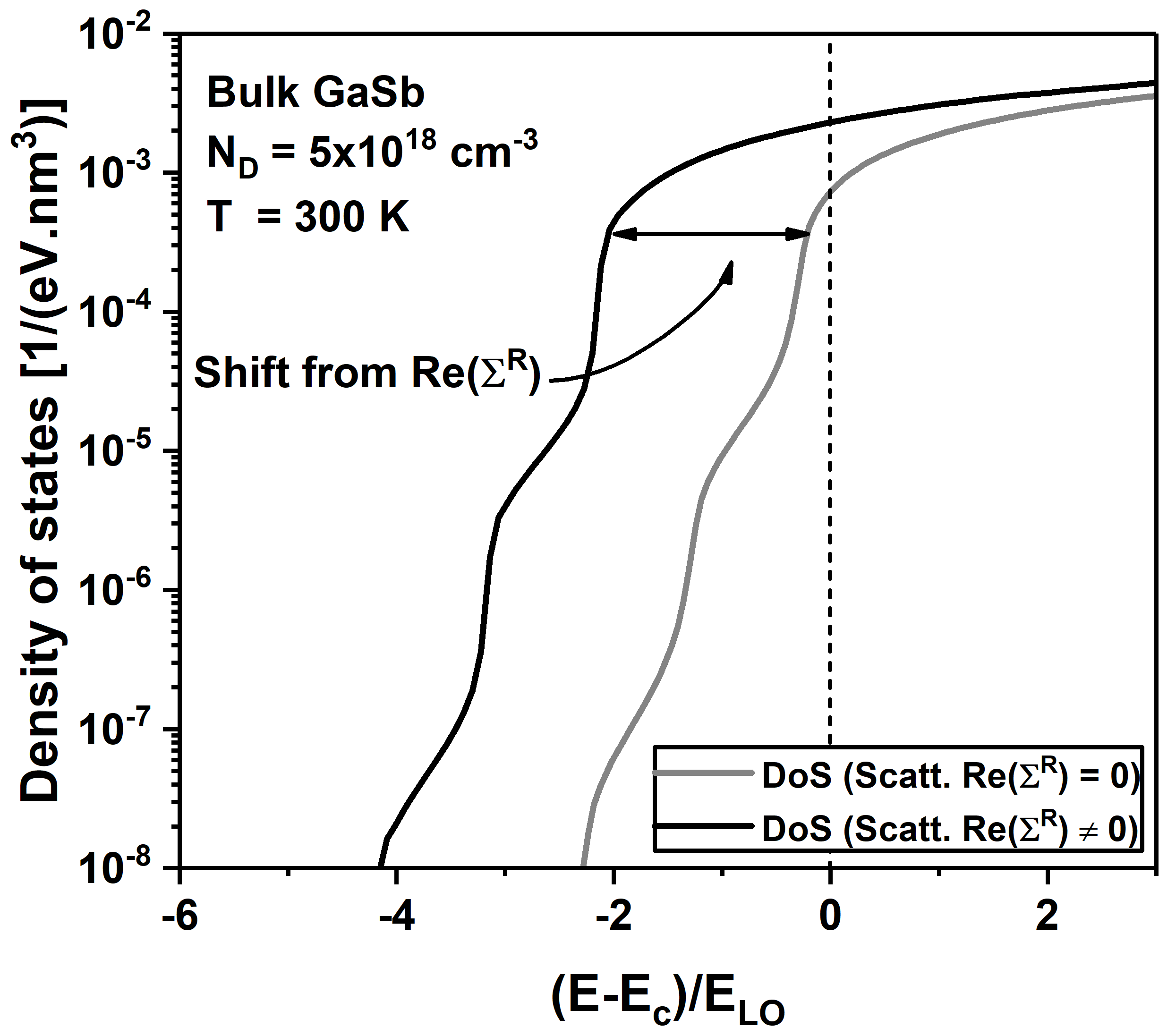
As detailed in Sec. II.3 and illustrated in Fig. 14, the band gap narrowing is deduced from two simulations - one with the real parts of all retarded scattering self-energies neglected and one with real part fully included. The band edge differences of the two simulations equals the band gap narrowing.
To verify this approach, the NEGF predictions of band gap narrowing are compared against published experimental data.
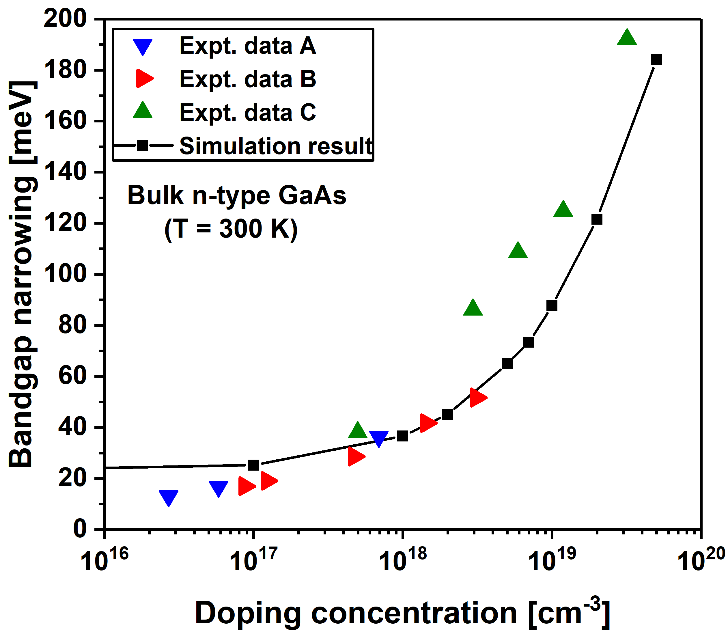
Figure 15 compares the simulated bandgap narrowing as a function of the doping concentration for bulk n-type GaAs with the experimental data of Refs. Yao and Compaan, 1990, Luo et al., 2002, and Harmon et al., 1994. The band gap narrowing increases with the doping concentration due to increasing impurity scattering. The simulation results show quantitative agreement with the experimental data for conduction band edge shift related band gap narrowing. The remaining deviations can originate from crystal defects, disorder and exciton interactions. Experiments show that valence band edge shifts narrow the band gap similarly as the conduction band. In contrast, the NEGF results of this work show only marginal changes of the valence band edges indicating that the approximation of a constant scalar screening length might be inappropriate for valence band changes (for further discussion please see Ref. Oschlies et al. (1992)).
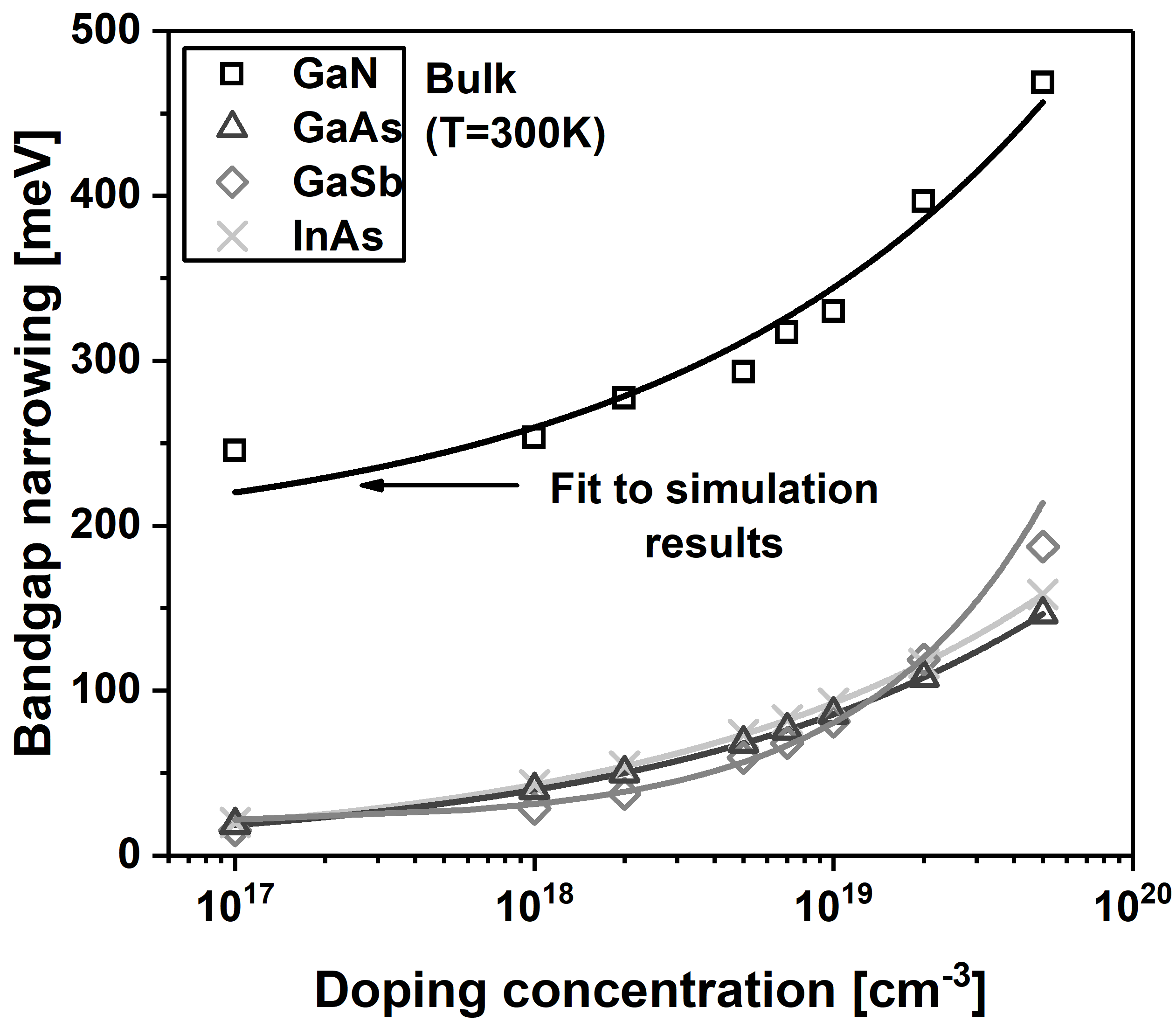
Figure 16 shows the conduction band induced band gap narrowing of GaN, GaAs, InAs and GaN as a function of the n-type doping concentration. All materials follow similar trends. GaN, has a larger band gap response due to the large phonon energy and the larger scattering potential compared to the other materials. Similar to the Urbach parameter, the variation of the band gap narrowing with doping can be fit with . Fig. 11). We follow e.g. Refs. Jain et al., 1990; Jain and Roulston, 1991; Lee et al., 1995 in using a polynomial fit function for the Urbach parameters and band gap narrowing. The corresponding fit parameters are summarized in Table 3.
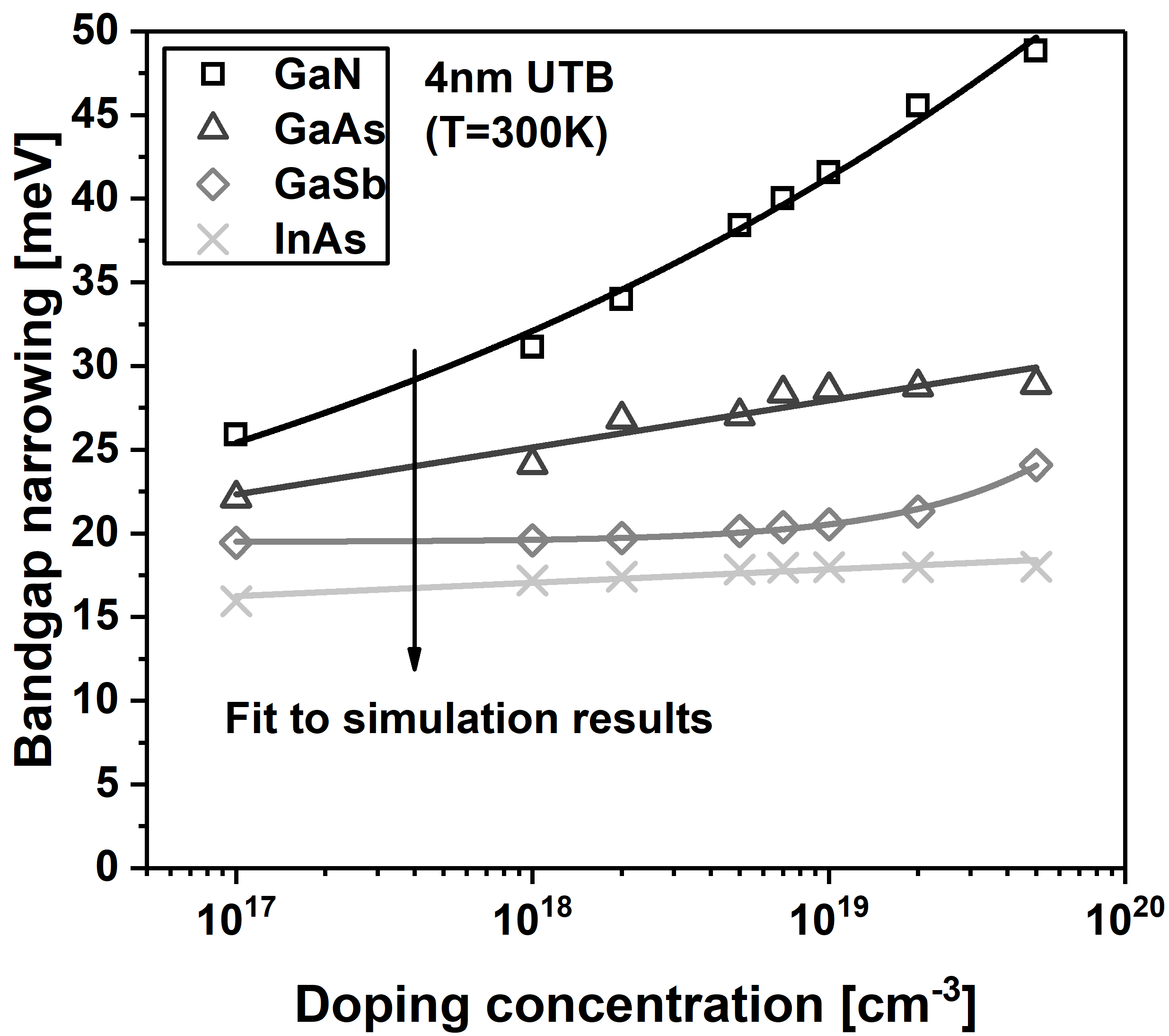
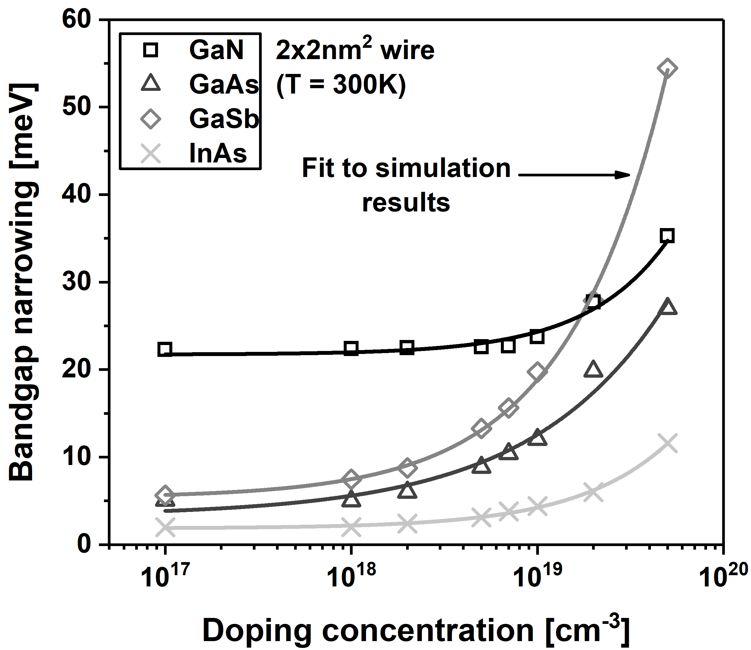
The band gap narrowing for GaN, GaAs, InAs and GaN UTBs and nanowires as a function of the doping concentration are shown in Figs. 17 and 18. Though the trend is similar in all three scenarios, the detailed doping dependence varies in bulk, UTBs and nanowires. This is similar to the scaling exponent of the Urbach parameter fit in Table 2.
| GaN | GaAs | GaSb | InAs | |
|---|---|---|---|---|
| Bulk | ||||
| 4nm UTB | ||||
| 22 wire |
IV Conclusion
This work introduces self-energy formulas for bulk, nanowire, and ultra-thin body electrons scattering on 3D polar optical phonons and uniformly distributed charged impurities in the multi-band tight binding representation. As often done, nonlocality of the scattering self-energies is limited to avoid unfeasible numerical load. This underestimation of scattering is compensated with a scaling factor that is deduced from Fermi’s golden rule prior to the actual NEGF calculations. Band tails and band gap narrowing in GaAs, InAs, GaSb and GaN as well as in UTBs and nanowires of the same materials is predicted with NEGF in the self-consistent Born approximation. The extracted Urbach tail parameter as well as the conduction band driven band gap narrowing agrees quantitatively with available experimental data. This is also true for their dependence on the doping concentration. A polynomial fit to the simulated Urbach tails and band gaps eases interpolating predictions from this work for bulk, UTBs and nanowires for different doping concentrations.
V Acknowledgements
James Charles and Tillmann Kubis acknowledge support by the Silvaco Inc. This work was partly supported by the Semiconductor Research Corporations Global Research Collaboration (GRC) (2653.001). This research was supported in part through computational resources provided by Information Technology at Purdue, West Lafayette, Indiana. The authors acknowledge the Texas Advanced Computing Center (TACC) at The University of Texas at Austin for providing HPC resources that have contributed to the research results reported within this paper. This research used resources of the Oak Ridge Leadership Computing Facility, which is a DOE Office of Science User Facility supported under Contract DE-AC05-00OR22725.
References
- Lind et al. (2015) E. Lind, E. Memišević, A. W. Dey, and L.-E. Wernersson, Iii-v heterostructure nanowire tunnel fets, IEEE Journal of the Electron Devices Society 3, 96 (2015).
- Avci et al. (2015) U. E. Avci, D. H. Morris, and I. A. Young, Tunnel field-effect transistors: Prospects and challenges, IEEE J. Electron Devices Soc. 3, 88 (2015).
- Seabaugh and Zhang (2010) A. C. Seabaugh and Q. Zhang, Low-voltage tunnel transistors for beyond cmos logic, Proceedings of the IEEE 98, 2095 (2010).
- Geng et al. (2018) J. Geng, P. Sarangapani, K.-C. Wang, E. Nelson, B. Browne, C. Wordelman, J. Charles, Y. Chu, T. Kubis, and G. Klimeck, Quantitative multi-scale, multi-physics quantum transport modeling of gan-based light emitting diodes, physica status solidi (a) 215, 1700662 (2018).
- Laubsch et al. (2010) A. Laubsch, M. Sabathil, J. Baur, M. Peter, and B. Hahn, High-power and high-efficiency ingan-based light emitters, IEEE transactions on electron devices 57, 79 (2010).
- Guo et al. (2010) W. Guo, M. Zhang, A. Banerjee, and P. Bhattacharya, Catalyst-free ingan/gan nanowire light emitting diodes grown on (001) silicon by molecular beam epitaxy, Nano letters 10, 3355 (2010).
- Krogstrup et al. (2013) P. Krogstrup, H. I. Jørgensen, M. Heiss, O. Demichel, J. V. Holm, M. Aagesen, J. Nygard, and A. F. i Morral, Single-nanowire solar cells beyond the shockley–queisser limit, Nature Photonics 7, 306 (2013).
- Bailey et al. (2011) C. G. Bailey, D. V. Forbes, R. P. Raffaelle, and S. M. Hubbard, Near 1 v open circuit voltage inas/gaas quantum dot solar cells, Applied Physics Letters 98, 163105 (2011).
- Wallentin et al. (2013) J. Wallentin, N. Anttu, D. Asoli, M. Huffman, I. Åberg, M. H. Magnusson, G. Siefer, P. Fuss-Kailuweit, F. Dimroth, B. Witzigmann, et al., Inp nanowire array solar cells achieving 13.8% efficiency by exceeding the ray optics limit, Science , 1230969 (2013).
- Agarwal and Yablonovitch (2014) S. Agarwal and E. Yablonovitch, Band-edge steepness obtained from esaki/backward diode current–voltage characteristics, IEEE Transactions on Electron Devices 61, 1488 (2014).
- Bizindavyi et al. (2018) J. Bizindavyi, A. S. Verhulst, Q. Smets, D. Verreck, B. Sorée, and G. Groeseneken, Band-tails tunneling resolving the theory-experiment discrepancy in esaki diodes, IEEE Journal of the Electron Devices Society 6, 633 (2018).
- Lu and Seabaugh (2014) H. Lu and A. Seabaugh, Tunnel field-effect transistors: State-of-the-art, IEEE Journal of the Electron Devices Society 2, 44 (2014).
- Oehme et al. (2013) M. Oehme, M. Gollhofer, D. Widmann, M. Schmid, M. Kaschel, E. Kasper, and J. Schulze, Direct bandgap narrowing in ge led’s on si substrates, Optics express 21, 2206 (2013).
- Halperin and Lax (1966) B. Halperin and M. Lax, Impurity-band tails in the high-density limit. i. minimum counting methods, Physical Review 148, 722 (1966).
- Halperin and Lax (1967) B. Halperin and M. Lax, Impurity-band tails in the high-density limit. ii. higher order corrections, Physical Review 153, 802 (1967).
- John et al. (1986) S. John, C. Soukoulis, M. H. Cohen, and E. Economou, Theory of electron band tails and the urbach optical-absorption edge, Physical review letters 57, 1777 (1986).
- Jain and Roulston (1991) S. Jain and D. Roulston, A simple expression for band gap narrowing (bgn) in heavily doped si, ge, gaas and gexsi1- x strained layers, Solid-State Electronics 34, 453 (1991).
- Zhang et al. (2016) H. Zhang, W. Cao, J. Kang, and K. Banerjee, in Electron Devices Meeting (IEDM), 2016 IEEE International (IEEE, 2016) pp. 30–3.
- Datta (2000) S. Datta, Nanoscale device modeling: the green’s function method, Superlattices and microstructures 28, 253 (2000).
- Lake et al. (1997) R. Lake, G. Klimeck, R. C. Bowen, and D. Jovanovic, Single and multiband modeling of quantum electron transport through layered semiconductor devices, Journal of Applied Physics 81, 7845 (1997).
- Markussen et al. (2009) T. Markussen, A.-P. Jauho, and M. Brandbyge, Electron and phonon transport in silicon nanowires: Atomistic approach to thermoelectric properties, Physical Review B 79, 035415 (2009).
- Lee and Wacker (2002) S.-C. Lee and A. Wacker, Nonequilibrium green’s function theory for transport and gain properties of quantum cascade structures, Physical Review B 66, 245314 (2002).
- Steiger (2009) S. Steiger, Modelling nano-LEDs, Ph.D. thesis (2009).
- Kubis et al. (2009) T. Kubis, C. Yeh, P. Vogl, A. Benz, G. Fasching, and C. Deutsch, Theory of nonequilibrium quantum transport and energy dissipation in terahertz quantum cascade lasers, Physical Review B 79, 195323 (2009).
- Luisier and Klimeck (2009) M. Luisier and G. Klimeck, Atomistic full-band simulations of silicon nanowire transistors: Effects of electron-phonon scattering, Physical Review B 80, 155430 (2009).
- Afzalian et al. (2018) A. Afzalian, T. Vasen, P. Ramvall, T. Shen, J. Wu, and M. Passlack, Physics and performances of iii–v nanowire broken-gap heterojunction tfets using an efficient tight-binding mode-space negf model enabling million-atom nanowire simulations, Journal of Physics: Condensed Matter 30, 254002 (2018).
- Ameen et al. (2017) T. A. Ameen, H. Ilatikhameneh, J. Z. Huang, M. Povolotskyi, R. Rahman, and G. Klimeck, Combination of equilibrium and nonequilibrium carrier statistics into an atomistic quantum transport model for tunneling heterojunctions, IEEE Transactions on Electron Devices 64, 2512 (2017).
- Bowen et al. (1997) R. C. Bowen, G. Klimeck, R. K. Lake, W. R. Frensley, and T. Moise, Quantitative simulation of a resonant tunneling diode, Journal of applied physics 81, 3207 (1997).
- Sarangapani et al. (2018) P. Sarangapani, C. Weber, J. Chang, S. Cea, M. Povolotskyi, G. Klimeck, and T. Kubis, Atomistic tight-binding study of contact resistivity in si/sige pmos schottky contacts, IEEE Transactions on Nanotechnology (2018).
- Hegde and Chris Bowen (2014) G. Hegde and R. Chris Bowen, Effect of realistic metal electronic structure on the lower limit of contact resistivity of epitaxial metal-semiconductor contacts, Applied Physics Letters 105, 053511 (2014).
- Miao et al. (2016) K. Miao, S. Sadasivam, J. Charles, G. Klimeck, T. Fisher, and T. Kubis, Büttiker probes for dissipative phonon quantum transport in semiconductor nanostructures, Applied Physics Letters 108, 113107 (2016).
- Riddoch and Ridley (1983) F. Riddoch and B. Ridley, On the scattering of electrons by polar optical phonons in quasi-2d quantum wells, Journal of Physics C: Solid State Physics 16, 6971 (1983).
- Fischetti and Laux (1988) M. V. Fischetti and S. E. Laux, Monte carlo analysis of electron transport in small semiconductor devices including band-structure and space-charge effects, Physical Review B 38, 9721 (1988).
- Steiger et al. (2011) S. Steiger, M. Povolotskyi, H.-H. Park, T. Kubis, and G. Klimeck, Nemo5: A parallel multiscale nanoelectronics modeling tool, IEEE Transactions on Nanotechnology 10, 1464 (2011).
- Klimeck et al. (2000) G. Klimeck, R. Bowen, T. Boykin, and T. Cwik, in APS Meeting Abstracts (2000).
- Jancu et al. (2002) J.-M. Jancu, F. Bassani, F. D. Sala, and R. Scholz, Transferable tight-binding parametrization for the group-iii nitrides, Applied physics letters 81, 4838 (2002).
- Brooks (1951) H. Brooks, in Physical Review, Vol. 83 (AMERICAN PHYSICAL SOC ONE PHYSICS ELLIPSE, COLLEGE PK, MD 20740-3844 USA, 1951) pp. 879–879.
- Lindhard (1954) J. Lindhard, On the properties of a gas of charged particles, Dan. Vid. Selsk Mat.-Fys. Medd. 28, 8 (1954).
- Fröhlich (1952) H. Fröhlich, Interaction of electrons with lattice vibrations, Proc. R. Soc. Lond. A 215, 291 (1952).
- Lan (a) Gallium nitride (gan) dielectric constants: Datasheet from landolt-börnstein - group iii condensed matter · volume 41a1: “group iv elements, iv-iv and iii-v compounds. part a - lattice properties” in springermaterials (https://dx.doi.org/10.1007/10551045_87), (a), copyright 2001 Springer-Verlag Berlin Heidelberg.
- Strauch (a) D. Strauch, Gan: phonon frequencies: Datasheet from landolt-börnstein - group iii condensed matter · volume 44d: “new data and updates for iv-iv, iii-v, ii-vi and i-vii compounds, their mixed crystals and diluted magnetic semiconductors” in springermaterials (https://dx.doi.org/10.1007/978-3-642-14148-5_222), (a), copyright 2011 Springer-Verlag Berlin Heidelberg.
- Strauch (b) D. Strauch, Gaas: phonon dispersion curves, phonon density of states, phonon frequencies: Datasheet from landolt-börnstein - group iii condensed matter · volume 44d: “new data and updates for iv-iv, iii-v, ii-vi and i-vii compounds, their mixed crystals and diluted magnetic semiconductors” in springermaterials (https://dx.doi.org/10.1007/978-3-642-14148-5_102), (b), copyright 2011 Springer-Verlag Berlin Heidelberg.
- (43) Gaas rt permittivity (dielectric constant): Datasheet from “pauling file multinaries edition – 2012” in springermaterials (https://materials.springer.com/isp/physical-property/docs/ppp_5b220e9b7c082d4f92d21887a4be91a0), Copyright 2016 Springer-Verlag Berlin Heidelberg & Material Phases Data System (MPDS), Switzerland & National Institute for Materials Science (NIMS), Japan.
- Lan (b) Gallium antimonide (gasb) phonon dispersion, wavenumbers and frequencies: Datasheet from landolt-börnstein - group iii condensed matter · volume 41a1: “group iv elements, iv-iv and iii-v compounds. part a - lattice properties” in springermaterials (https://dx.doi.org/10.1007/10551045_118), (b), copyright 2001 Springer-Verlag Berlin Heidelberg.
- Lan (c) Gallium antimonide (gasb) dielectric constants: Datasheet from landolt-börnstein - group iii condensed matter · volume 41a1: “group iv elements, iv-iv and iii-v compounds. part a - lattice properties” in springermaterials (https://dx.doi.org/10.1007/10551045_124), (c), copyright 2001 Springer-Verlag Berlin Heidelberg.
- Lan (d) Indium arsenide (inas), dependence of phonons on uniaxial stress: Datasheet from landolt-börnstein - group iii condensed matter · volume 41a1: “group iv elements, iv-iv and iii-v compounds. part b - electronic, transport, optical and other properties” in springermaterials (https://dx.doi.org/10.1007/10832182_356), (d), copyright 2002 Springer-Verlag Berlin Heidelberg.
- (47) E. C. Fernandes da Silva, Inas: dielectric constant: Datasheet from landolt-börnstein - group iii condensed matter · volume 44c: “new data and updates for iii-v, ii-vi and i-vii compounds” in springermaterials (https://dx.doi.org/10.1007/978-3-540-92140-0_163), Copyright 2010 Springer-Verlag Berlin Heidelberg.
- Wacker (2002) A. Wacker, Semiconductor superlattices: a model system for nonlinear transport, Physics Reports 357, 1 (2002).
- Esposito et al. (2009) A. Esposito, M. Frey, and A. Schenk, Quantum transport including nonparabolicity and phonon scattering: application to silicon nanowires, Journal of computational electronics 8, 336 (2009).
- Goodnick and Lugli (1988) S. Goodnick and P. Lugli, Effect of electron-electron scattering on nonequilibrium transport in quantum-well systems, Physical Review B 37, 2578 (1988).
- Aeberhard (2019) U. Aeberhard, Challenges in the negf simulation of quantum-well photovoltaics posed by non-locality and localization, physica status solidi (b) , 1800500 (2019).
- Datta (2005) S. Datta, Quantum transport: atom to transistor (Cambridge university press, 2005).
- Tan et al. (2015) Y. P. Tan, M. Povolotskyi, T. Kubis, T. B. Boykin, and G. Klimeck, Tight-binding analysis of si and gaas ultrathin bodies with subatomic wave-function resolution, Physical Review B 92, 085301 (2015).
- Dow and Redfield (1972) J. D. Dow and D. Redfield, Toward a unified theory of urbach’s rule and exponential absorption edges, Physical Review B 5, 594 (1972).
- Khayer and Lake (2011) M. A. Khayer and R. K. Lake, Effects of band-tails on the subthreshold characteristics of nanowire band-to-band tunneling transistors, Journal of Applied Physics 110, 074508 (2011).
- Antonioli et al. (1981) G. Antonioli, D. Bianchi, and P. Franzosi, Intrinsic urbach rule and electron—phonon interaction in gaas and related iii-v compounds, physica status solidi (b) 106, 79 (1981).
- Johnson and Tiedje (1995) S. Johnson and T. Tiedje, Temperature dependence of the urbach edge in gaas, Journal of applied physics 78, 5609 (1995).
- Chichibu et al. (1997) S. Chichibu, T. Mizutani, T. Shioda, H. Nakanishi, T. Deguchi, T. Azuhata, T. Sota, and S. Nakamura, Urbach–martienssen tails in a wurtzite gan epilayer, Applied physics letters 70, 3440 (1997).
- Jain et al. (1990) S. Jain, J. McGregor, and D. Roulston, Band-gap narrowing in novel iii-v semiconductors, Journal of applied physics 68, 3747 (1990).
- Lee et al. (1995) N.-Y. Lee, K.-J. Lee, C. Lee, J.-E. Kim, H. Y. Park, D.-H. Kwak, H.-C. Lee, and H. Lim, Determination of conduction band tail and fermi energy of heavily si-doped gaas by room-temperature photoluminescence, Journal of applied physics 78, 3367 (1995).
- Yao and Compaan (1990) H. Yao and A. Compaan, Plasmons, photoluminescence, and band-gap narrowing in very heavily doped n-gaas, Applied Physics Letters 57, 147 (1990).
- Luo et al. (2002) H. Luo, W. Shen, Y. Zhang, and H. Yang, Study of band gap narrowing effect in n-gaas for the application of far-infrared detection, Physica B: Condensed Matter 324, 379 (2002).
- Harmon et al. (1994) E. Harmon, M. Melloch, and M. Lundstrom, Effective band-gap shrinkage in gaas, Applied physics letters 64, 502 (1994).
- Oschlies et al. (1992) A. Oschlies, R. Godby, and R. Needs, First-principles self-energy calculations of carrier-induced band-gap narrowing in silicon, Physical Review B 45, 13741 (1992).