Near-unity indistinguishability single photon source for large-scale
integrated quantum optics
Abstract
Integrated single photon sources are key building blocks for realizing scalable devices for quantum information processing. For such applications highly coherent and indistinguishable single photons on a chip are required. Here we report on a triggered resonance fluorescence single photon source based on In(Ga)As/GaAs quantum dots coupled to single- and multi-mode ridge waveguides. We demonstrate the generation of highly linearly polarized resonance fluorescence photons with 99.1% (96.0%) single-photon purity and 97.5% (95.0%) indistinguishability in case of multi-mode (single-mode) waveguide devices fulfilling the strict requirements imposed by multi-interferometric quantum optics applications. Our integrated triggered single photon source can be readily scaled up, promising a realistic pathway for on-chip linear optical quantum simulation, quantum computation and quantum networks.
pacs:
85.35.Be, 42.50.Ar, 42.82.-m, 42.50.DvLarge scale implementations of quantum information processing (QIP) schemes are one of the major challenges of modern quantum physics. Building a platform successfully combing many qubits is a very demanding task, however it would provide a system capable to perform quantum simulations, quantum computing and secure quantum communication. In this regard, using single photons as qubits is a particularly appealing concept. Due to the photons low decoherence and the inherent possibility of low-loss transmission, they can be used for both quantum computing and quantum communication applications Kok and Lovett (2010). Over the last decade, there have been extensive experimental efforts towards realizing large-scale optical QIP systems. A vast majority of these implementations, such as linear optics quantum computing Knill et al. (2001), boson sampling Spring et al. (2013) or quantum repeater schemes Briegel et al. (1998) involve a two-photon interference effect, where a complete wave-packet overlap of single photons at the beam splitter is required. This feature demands photons, which are indistinguishable in terms of energy, bandwidth, polarization and arrival time at the beam splitter. Consequently, sources of indistinguishable single photons are one of the central resources for a large scale experimental realization of the optical QIP devices.
Among different kinds of emitters quantum dots (QDs) coupled to photonic structures have been shown to be one of the brightest single photon sources (SPS) Santori et al. (2002); Aharonovich et al. (2016); Senellart et al. (2017), which under resonant excitation conditions Flagg et al. (2009); Ates et al. (2009); Senellart et al. (2017) can reach simultaneously indistinguishabilities higher than 95%, single photon purities better than 99% and extraction efficiencies as high as 65-79% Ding et al. (2016); Somaschi et al. (2016); Unsleber et al. (2016); Senellart et al. (2017); Fischer et al. (2016). Further, by applying advanced semiconductor micro-processing technologies it is possible to fabricate devices where QD electronic properties can be dynamically shaped by strain Zhang et al. (2016); Trotta et al. (2016) or electric Kiršanskė et al. (2017); Hoang et al. (2012) fields. The optical quality of such sources allowed already for demonstration of on-demand CNOT-gates Pooley et al. (2012); Gazzano et al. (2013); He et al. (2013), heralded entanglement between distant hole spins Delteil et al. (2015) or the recent realization of 3-,4- and 5-photon boson sampling Wang et al. (2017); Loredo et al. (2017).
It is believed that future steps towards large scale quantum optics should ensure the full on-chip scalability of SPSs Dietrich et al. (2016); Aharonovich et al. (2016). A natural system towards this goal are integrated circuits, where QD SPSs can be homogeneously Jöns et al. (2015); Enderlin et al. (2012); Schwagmann et al. (2011); Arcari et al. (2014); Reithmaier et al. (2015) or heterogeneously Davanco et al. (2017); Elshaari et al. (2017); Kim et al. (2017) integrated on a single chip. In this approach light can be directly coupled into in-plane waveguides (WGs) and combined with other functionalities on a chip such as phase shifters Midolo et al. (2017); Wang et al. (2014), beam splitters Prtljaga et al. (2014); Jöns et al. (2015); Kim et al. (2017), filters Elshaari et al. (2017); Harris et al. (2014), detectors Reithmaier et al. (2015); Kaniber et al. (2016) and other devices for light propagation, manipulation and detection on a single photon level.
By utilizing this idea near-unity coupling efficiency of a QD emitter to waveguide device was already achieved Lund-Hansen et al. (2008); Enderlin et al. (2012); Arcari et al. (2014); Stepanov et al. (2015), showing the undeniable potential of this concept. In addition, integrated circuits allow to spatially separate excitation and detection spots, which straightforwardly enables applying resonant driving schemes to slow-down decoherence processes and reduce on-demand emission time-jitter. This technique was already applied to waveguide integrated QDs under both continuous-wave Makhonin et al. (2014); Kalliakos et al. (2016) (CW) and pulsed Schwartz et al. (2016); Kiršanskė et al. (2017); Liu et al. (2018) excitation. In particular, two-photon interference of subsequently emitted resonance fluorescence photons have been demonstrated recently Kiršanskė et al. (2017); Liu et al. (2018), however recorded indistinguishability values failed to reach requirements imposed by quantum optics applications Pan et al. (2012).
One of the major issues in QD-based on-chip SPSs is the loss of photon indistinguishability related to the charge fluctuation from nearby etched surfaces Makhonin et al. (2014); Kalliakos et al. (2016). This is true especially for small in size, complex structures such as photonic crystal Liu et al. (2018) or nanobeam Kiršanskė et al. (2017) waveguides. To diminish this effect a number of strategies can be employed. Firstly, the amount of surface states could be decreased by optimizing passivation of the etched surfaces Press et al. (2010). Secondly, the charge environment could be stabilized by weak CW non-resonant optical illumination Majumdar et al. (2011) or gating Somaschi et al. (2016); Liu et al. (2018). Finally, the Purcell effect might be used to enhance the radiative emission rate and thus improve the photon indistinguishability in the presence of dephasing Somaschi et al. (2016); Ding et al. (2016); Unsleber et al. (2016); Liu et al. (2018); Iles-Smith et al. (2017). As we will show in this Letter, a simplified waveguide design with relatively large profile dimensions, keeping etched surfaces far away from QD, can be also very advantageous in this respect. By utilizing distributed Bragg reflectors (DBR) ridge waveguide design we fabricated SPSs which simultaneously meet the requirements of near perfect single photon purity and indistinguishability.
To evaluate the performance of our devices we performed resonance fluorescence experiments on In(Ga)As/GaAs QDs coupled to single-mode (SM) and multi-mode (MM) in-plane waveguides. The light confinement and guiding were achieved by DBRs in vertical and ridges defined in horizontal direction. Usage of DBRs WG instead of the GaAs WG slab approach allowed us to soften the waveguide profile dimensions allowing to achieve single-mode operation while keeping a relatively high QD-waveguide light coupling efficiency (14-19% into one WG arm). To simulate the integrated circuit device operation, the QDs were excited resonantly from top of the waveguides, and the emitted photons were collected from the side facets after up to 1 mm travel distance on a chip. Under such conditions a significant reduction of the scattered laser intensity was achieved, enabling our MM (SM) waveguide device generation of record high on-chip 97.5% (95.0%) indistinguishable triggered single photons with a 99.1% (96.0%) single-photon purity and over 99% (98%) linear polarization. We believe, that this integrated SPSs can be readily scaled up demonstrating a realistic pathway for on-chip optical quantum processing.
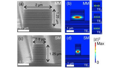
To realize our waveguide integrated SPS we have grown In(Ga)As/GaAs QDs embedded in a low-quality factor cavity (Q 200) based on DBRs. By performing three-dimensional finite-difference-time-domain (FDTD) calculations we investigated different waveguide designs for maximized coupling efficiency. We found that 1.25-1.65 m WG height and 0.6-2.0 m width lay within optimal values and allow to achieve around 10-22% coupling efficiency into each WG arm (total 20-44%). Moreover, our DBR waveguides can be operated in the single-mode regime for WG widths as small as 0.9 m at 900 nm cut-off wavelengths. Based on those considerations, we realized two types of ridge waveguides: (i) MM WGs with 2.0 x 1.25 m2 profile and (ii) SM WGs with 0.8 x 1.25 m2, for which we expect 14% and 19% QD coupling efficiency into one WG arm, respectively. We point out, that in principle the QD-emission coupling efficiency could be further improved by integration of DBR WGs with low-refractive-index layers while maintaining the mentioned relatively large size of WG profile. More details can be found in Supplemental Materials. Scanning electron microscope images of our fabricated MM and SM ridge waveguides are shown in Figures 1(a) and (c), respectively. Figures 1(b) and (d) show simulated optical mode profiles of the light field confined in our devices, calculated for the transverse-electric (TE) modes at 930 nm. In both cases the mode profiles are confined within the defined ridges, allowing for the single photon guiding along the chip. The modes are mainly concentrated in the GaAs cores and partially penetrate the top and bottom DBR mirrors.”
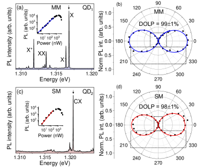
Initially, both devices were characterized optically under non-resonant excitation conditions. Figure 2(a) and (c) show side collected photoluminescence (PL) spectra from a QD1 and QD2, respectively, under above-bandgap CW pump (660 nm diode laser) from the top of the waveguide. In case of QD1 coupled to a MM WG four intense emission lines are visible, where the one of interest centered at 1.3169 eV (marked with an arrow) was identified as a neutral exciton (X). The inset in Fig. 2(a) shows central peak intensity changes vs excitation power indicating a clear linear dependence. The remaining emission lines have been identified based on power- and top-detected-polarization-resolved PL as positively charged exciton (X+), negatively charged exciton (X-) and biexciton (XX) recombination from the same QD. Spectra for QD2 coupled to the SM WG consists of a single emission line centered at 1.3206 eV, identified as a charged exciton (CX). Both studied emission lines show a high degree of linear polarization (DOLP) of around 991% and 981% for QD1 and QD2, respectively, oriented in sample plane as shown in Figures 2(b) and (d). A high DOLP and its direction are related to the QDs dipole moments, which are mainly in-plane oriented and thus emitted photons mostly couple to and propagate in the TE waveguide mode.
Next, the characteristics of the devices were probed under pulsed s-shell resonant excitation. Figures 3(a) and (d) show side detected pulsed resonance fluorescence spectra displayed on a spectrometer at a temperature of 4.5 K. Since in our experimental configuration the excitation and collection spots are spatially separated by hundreds of micrometers, it allows us to rather readily suppress the stray laser photons scattered from the excitation area. This is usually not the case for short length waveguides as the laser light scattered from the excitation area might be collected within the numerical aperture of the detection objective. Additionally, the presence of low Q factor cavity in the plane of the sample allowed us to more effectively excite the emitters and thus reduce powers needed for resonant driving. To further suppress the influence of laser light scattering on the single photon performance, the beam spot size, as well as polarization, was carefully controlled. By utilizing both the intrinsic (spatial separation) and polarization filtering we were able to obtain a signal-to-background (S/B) ratio of over 100 for MM and 30 for SM waveguide devices under -pulse excitation. In fact, we believe that polarization filtering can be omitted for fully on-chip device operation.
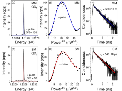
In Figures 3(b) and (e) the resonance fluorescence intensity versus the square root of the incident power are shown. Clear Rabi oscillations with visible damping for both QDs are observed, which is due to coherent control of the particular QD’s two-level systems coupled to phonon bath Förstner et al. (2003). The emission intensities in both cases reach the maximum for -pulse with laser powers of 440 nW and 160 W for QD1 and QD2, respectively. The significantly larger pump power required to reach -pulse for QD2 is most likely related to the smaller size of the waveguide in respect to the laser beam spot size, as well as a slight energy detuning from the planar cavity resonance. The resonance fluorescence intensity of around 10 kcps (3.5 kcps) was observed on the avalanche photodiode detector (setup efficiency 2%) at -pulse for a MM (SM) device, which corresponds to 0.6% (0.2%) total photon extraction efficiency from a QD collected by the first lens, and 12% (2%) coupling efficiency into one WG arm (lower bound estimated based on 95% and 90% losses due to the out-coupling). It needs to be noted that the design of the WGs for the high out-coupling into external collection optics was not optimized since ultimately all single photon processing is supposed to be performed on-chip. Under -pulse excitation the time-resolved resonance fluorescence measurements have been performed. The recorded fluorescence decay time traces shown in Fig. 3(c) and (f) demonstrate clear mono-exponential decays with the time constants of 50010 ps and 54010 ps for QD1 and QD2, respectively.
In order to characterize purity and indistinguishability of our SPSs auto-correlation and two-photon interference experiments have been performed on the resonance fluorescence signal filtered out from a broader laser profile and phonon sidebands. In Fig. 4(a) second-order correlation function histograms recorded in Hanbury Brown and Twiss (HBT) configuration under -pulse excitation for QD1 and QD2 are shown. In both cases, nearly vanishing multi-photon emission probabilities at zero delays have been recorded with and for QD1 and QD2, respectively. The shape of all the peaks exhibits a clear two-sided mono-exponential decay with a time constant corresponding to the decay time recorded directly in the time-resolved resonance fluorescence measurements.
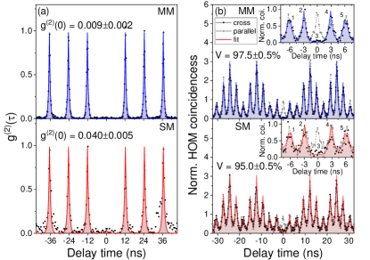
To study the indistinguishability of the emitted photons the QDs were excited twice every repetition cycle (12.2 ns) by a pair of pulses separated by 3 ns. Two subsequently emitted photons are then introduced into a 3 ns unbalanced interferometer where a delay between them is compensated in order to superimpose single photon pulses on the beam splitter Santori et al. (2002). If the two photons are perfectly indistinguishable they will always exit the same but a random output port, which is quantitatively translated into the two-coincidences correlation dip at a zero delay. Hong-Ou-Mandel (HOM) correlation histograms obtained for the two considered photon sources are presented in Figure 4(b) in upper (QD1) and lower (QD2) panels. The histograms consist of a set of five 3 ns delayed peak clusters separated by the repetition time of the laser (first and the last peak of the neighboring clusters are superimposed). The central cluster [insets in Figure 4(b)] describes coincidence events related to the single-photons traveling through different paths of the interferometer. This is described in detail in the Supplemental Materials. In order to evaluate the zero delay peak (no. 3) area with respect to the neighboring peaks (no. 2 and 4) the experimental data have been fitted with the two-side exponential decay functions. Upon this procedure, the two-photon HOM interference visibility of 0.9750.005 for QD1 and 0.9500.005 for QD2 have been obtained after correcting for HOM setup imperfections such as beam-splitting ratio (R/T = 1.15) and contrast of the Mach-Zehnder-interferometer (1- = 0.99)Santori et al. (2002); Fischer et al. (2016).
It was recently demonstrated, that single photon emission purity and indistinguishability in resonantly excited two-level systems is intrinsically limited by the re-excitation processHanschke et al. (2018); Fischer et al. (2016). Specifically, it was shown that the laser excitation pulse-length sets the lower bounds of the HBT and HOM experimental two-photon coincidences probability, and thus and visibility values obtainable for a given SPS with characteristic emission time . Based on reference Fischer et al. (2016) those bounds can be calculated following the linear dependence , which in our case limits (visibility) to 0.0016 (0.9984) and 0.0015 (0.9985) for QD1 and QD2, respectively. Since the experimentally obtained single-photon purity values are significantly above the aforementioned limits, we believe their dominant component might be non-filtered residual scatter of the laser pulse from the sample surface, which we do not take into account in HBT and HOM data analysis.
Imperfect efficiency and indistinguishability of SPSs are related to the problem of optical quantum computation under a degree of experimental error. There have been a number of promising proposals of linear optical quantum computing that are robust against imperfect SPSs and inefficient detectors. In particular, it was shown, that fault-tolerant quantum computation can be performed if the two-photon gate operation error probability is lower than a 1% threshold value Fowler et al. (2009); Knill (2005). In this regard, we can calculate how the indistinguishability of input photons affects the two-photon gate performance assuming perfect beam-overlap, alignment, beam-splitters and no dark counts in single photon counting detection. In case of our MM (SM) waveguide QD source with 97.5% (95.0%) photons visibility a gate fidelity of 99.5% (99.1%) Wei et al. (2014) is theoretically obtainable. Those values already surpass mentioned 1% precision threshold value, and in this context, our work provides SPSs with photons visibility needed for scalable quantum technologies.
Another source of error in quantum optics, which is far more dominant than gate fidelity is photon loss. This problem is associated with the overall source and detectors efficiency, which product has to be greater than 2/3 in order to perform efficient fault-tolerant linear optical quantum computation Varnava et al. (2008). In principle, this efficiency threshold is very difficult to fulfill in any system, since every optical setup exhibit losses. In all on-chip platforms however, where single photons are generated, routed, manipulated and eventually detected within the same low loss photonic circuit, this efficiency threshold is likely to be fulfilled within the near future.
In this context, essential next steps to make QD-based on-chip platform feasible for fully scalable quantum technologies would consist of (i) improving QD-waveguide circuit coupling efficiency while maintaining high degree of photons indistinguishability, (ii) introducing high-visibility and low-loss on-chip interferometers and phase shifters based on single-mode waveguides, and (iii) integrating with high efficiency superconducting detectors Dietrich et al. (2016); Aharonovich et al. (2016); Senellart et al. (2017). Such a system may at some point overcome the intrinsic limitations of the vertical devices, opening the possibility to create a scalable quantum integrated circuits operating at the single photon level.
In this Letter, we have shown that our MM (SM) waveguide integrated SPS can generate photons with near-unity indistinguishability of 0.9750.005 (0.9500.005) along with the value equal to 0.0090.002 (0.0400.005). We demonstrated single photon propagation of over hundreds of micrometers in waveguides and QD-WG coupling efficiency of 12% (2%) into one WG arm. In contrast to any other QD-based waveguide integrated SPS which has been demonstrated thus far Kiršanskė et al. (2017); Liu et al. (2018), our devices fulfill ultimate single photon purity and indistinguishability demands, imposed by boson sampling and linear optical quantum computing applications Pan et al. (2012). Performance of this source already outperforms any other on-chip integrated emitters including state-of-the-art heralded single photon spontaneous parametric down-conversion sources, where a maximum of 91% photons indistinguishability has been achieved at 4-5% source efficiency Wang et al. (2016); Kaneda and Kwiat (2018). We believe that our device could be straightforwardly integrated with advanced on-chip functionalities including reconfigurable and reprogrammable optical circuits Carolan et al. (2015) suitable for handling large scale multi-photon experiments. A potential of manufacturing such advanced quantum circuits combined with high purity indistinguishable SPS open a route towards fully integrated and thus scalable quantum information processing.
Acknowledgements.
The authors thank Silke Kuhn for fabricating the structures, and Dominick Köck for calculating the electric field distribution in waveguides. Ł.D. acknowledges the financial support from the Alexander von Humboldt Foundation. S.-H.K. acknowledges the financial support from the National Research Foundation of Korea through the Korean Government Grant NRF-2016R1C1B2007007. We are furthermore grateful for the support by the State of Bavaria.References
- Kok and Lovett (2010) P. Kok and B. Lovett, Introduction to Optical Quantum Information Processing (Cambridge University Press, 2010).
- Knill et al. (2001) E. Knill, R. Laflamme, and G. J. Milburn, Nature 409, 46 (2001).
- Spring et al. (2013) J. B. Spring, B. J. Metcalf, P. C. Humphreys, W. S. Kolthammer, X.-M. Jin, M. Barbieri, A. Datta, N. Thomas-Peter, N. K. Langford, D. Kundys, J. C. Gates, B. J. Smith, P. G. R. Smith, and I. A. Walmsley, Science 339, 798 (2013).
- Briegel et al. (1998) H.-J. Briegel, W. Dür, J. I. Cirac, and P. Zoller, Physical Review Letters 81, 5932 (1998).
- Santori et al. (2002) C. Santori, D. Fattal, J. Vucković, G. S. Solomon, and Y. Yamamoto, Nature 419, 594 (2002).
- Aharonovich et al. (2016) I. Aharonovich, D. Englund, and M. Toth, Nature Photonics 10, 631 (2016).
- Senellart et al. (2017) P. Senellart, G. Solomon, and A. White, Nature Nanotechnology 12, 1026 (2017).
- Flagg et al. (2009) E. B. Flagg, A. Muller, J. W. Robertson, S. Founta, D. G. Deppe, M. Xiao, W. Ma, G. J. Salamo, and C. K. Shih, Nature Physics 5, 203 (2009).
- Ates et al. (2009) S. Ates, S. M. Ulrich, S. Reitzenstein, A. Löffler, A. Forchel, and P. Michler, Physical Review Letters 103, 167402 (2009).
- Ding et al. (2016) X. Ding, Y. He, Z. C. Duan, N. Gregersen, M. C. Chen, S. Unsleber, S. Maier, C. Schneider, M. Kamp, S. Höfling, C.-Y. Lu, and J.-W. Pan, Physical Review Letters 116, 020401 (2016).
- Somaschi et al. (2016) N. Somaschi, V. Giesz, L. De Santis, J. C. Loredo, M. P. Almeida, G. Hornecker, S. L. Portalupi, T. Grange, C. Antón, J. Demory, C. Gómez, I. Sagnes, N. D. Lanzillotti-Kimura, A. Lemaítre, A. Auffeves, A. G. White, L. Lanco, and P. Senellart, Nature Photonics 10, 340 (2016).
- Unsleber et al. (2016) S. Unsleber, Y.-M. He, S. Maier, S. Gerhardt, C.-Y. Lu, J.-W. Pan, M. Kamp, C. Schneider, and S. Höfling, Optics express 24, 8539 (2016).
- Fischer et al. (2016) K. A. Fischer, K. Müller, K. G. Lagoudakis, and J. Vučković, New Journal of Physics 18, 113053 (2016).
- Zhang et al. (2016) Y. Zhang, Y. Chen, M. Mietschke, L. Zhang, F. Yuan, S. Abel, R. Hühne, K. Nielsch, J. Fompeyrine, F. Ding, and O. G. Schmidt, Nano Letters 16, 5785 (2016).
- Trotta et al. (2016) R. Trotta, J. Martín-Sánchez, J. S. Wildmann, G. Piredda, M. Reindl, C. Schimpf, E. Zallo, S. Stroj, J. Edlinger, and A. Rastelli, Nature Communications 7, 10375 (2016).
- Kiršanskė et al. (2017) G. Kiršanskė, H. Thyrrestrup, R. S. Daveau, C. L. Dreeßen, T. Pregnolato, L. Midolo, P. Tighineanu, A. Javadi, S. Stobbe, R. Schott, A. Ludwig, A. D. Wieck, S. I. Park, J. D. Song, A. V. Kuhlmann, I. Söllner, M. C. Löbl, R. J. Warburton, and P. Lodahl, Physical Review B 96, 165306 (2017).
- Hoang et al. (2012) T. B. Hoang, J. Beetz, M. Lermer, L. Midolo, M. Kamp, S. Höfling, and A. Fiore, Optics Express 20, 21758 (2012).
- Pooley et al. (2012) M. A. Pooley, D. J. P. Ellis, R. B. Patel, A. J. Bennett, K. H. A. Chan, I. Farrer, D. A. Ritchie, and A. J. Shields, Applied Physics Letters 100, 211103 (2012).
- Gazzano et al. (2013) O. Gazzano, M. P. Almeida, A. K. Nowak, S. L. Portalupi, A. Lemaître, I. Sagnes, A. G. White, and P. Senellart, Physical Review Letters 110, 250501 (2013).
- He et al. (2013) Y.-M. He, Y. He, Y.-J. Wei, D. Wu, M. Atatüre, C. Schneider, S. Höfling, M. Kamp, C.-Y. Lu, and J.-W. Pan, Nature Nanotechnology 8, 213 (2013).
- Delteil et al. (2015) A. Delteil, Z. Sun, W.-b. Gao, E. Togan, S. Faelt, and A. Imamoğlu, Nature Physics 12, 218 (2015).
- Wang et al. (2017) H. Wang, Y.-M. He, Y.-H. Li, Z.-E. Su, B. Li, H.-L. Huang, X. Ding, M.-C. Chen, C. Liu, J. Qin, J.-P. Li, Y.-M. He, C. Schneider, M. Kamp, C.-Z. Peng, S. Höfling, C.-Y. Lu, and J.-W. Pan, Nature Photonics 11, 361 (2017).
- Loredo et al. (2017) J. C. Loredo, M. A. Broome, P. Hilaire, O. Gazzano, I. Sagnes, A. Lemaitre, M. P. Almeida, P. Senellart, and A. G. White, Physical Review Letters 118, 130503 (2017).
- Dietrich et al. (2016) C. P. Dietrich, A. Fiore, M. G. Thompson, M. Kamp, and S. Höfling, Laser & Photonics Reviews 10, 870 (2016).
- Jöns et al. (2015) K. D. Jöns, U. Rengstl, M. Oster, F. Hargart, M. Heldmaier, S. Bounouar, S. M. Ulrich, M. Jetter, and P. Michler, Journal of Physics D: Applied Physics 48, 085101 (2015).
- Enderlin et al. (2012) A. Enderlin, Y. Ota, R. Ohta, N. Kumagai, S. Ishida, S. Iwamoto, and Y. Arakawa, Physical Review B 86, 075314 (2012).
- Schwagmann et al. (2011) A. Schwagmann, S. Kalliakos, I. Farrer, J. P. Griffiths, G. A. C. Jones, D. A. Ritchie, and A. J. Shields, Applied Physics Letters 99, 261108 (2011).
- Arcari et al. (2014) M. Arcari, I. Söllner, A. Javadi, S. Lindskov Hansen, S. Mahmoodian, J. Liu, H. Thyrrestrup, E. H. Lee, J. D. Song, S. Stobbe, and P. Lodahl, Physical Review Letters 113, 093603 (2014).
- Reithmaier et al. (2015) G. Reithmaier, M. Kaniber, F. Flassig, S. Lichtmannecker, K. Müller, A. Andrejew, J. Vučković, R. Gross, and J. J. Finley, Nano Letters 15, 5208 (2015).
- Davanco et al. (2017) M. Davanco, J. Liu, L. Sapienza, C.-Z. Zhang, J. V. De Miranda Cardoso, V. Verma, R. Mirin, S. W. Nam, L. Liu, and K. Srinivasan, Nature Communications 8, 889 (2017).
- Elshaari et al. (2017) A. W. Elshaari, I. E. Zadeh, A. Fognini, M. E. Reimer, D. Dalacu, P. J. Poole, V. Zwiller, and K. D. Jöns, Nature Communications 8, 379 (2017).
- Kim et al. (2017) J.-H. Kim, S. Aghaeimeibodi, C. J. K. Richardson, R. P. Leavitt, D. Englund, and E. Waks, Nano Letters 17, 7394 (2017).
- Midolo et al. (2017) L. Midolo, S. L. Hansen, W. Zhang, C. Papon, R. Schott, A. Ludwig, A. D. Wieck, P. Lodahl, and S. Stobbe, Opt. Express 25, 33514 (2017).
- Wang et al. (2014) J. Wang, A. Santamato, P. Jiang, D. Bonneau, E. Engin, J. W. Silverstone, M. Lermer, J. Beetz, M. Kamp, S. Höfling, M. G. Tanner, C. M. Natarajan, R. H. Hadfield, S. N. Dorenbos, V. Zwiller, J. L. O’Brien, and M. G. Thompson, Optics Communications 327, 49 (2014).
- Prtljaga et al. (2014) N. Prtljaga, R. J. Coles, J. O’Hara, B. Royall, E. Clarke, A. M. Fox, and M. S. Skolnick, Applied Physics Letters 104, 231107 (2014).
- Harris et al. (2014) N. C. Harris, D. Grassani, A. Simbula, M. Pant, M. Galli, T. Baehr-Jones, M. Hochberg, D. Englund, D. Bajoni, and C. Galland, Physical Review X 4, 041047 (2014).
- Kaniber et al. (2016) M. Kaniber, F. Flassig, G. Reithmaier, R. Gross, and J. J. Finley, Applied Physics B 122, 115 (2016).
- Lund-Hansen et al. (2008) T. Lund-Hansen, S. Stobbe, B. Julsgaard, H. Thyrrestrup, T. Sünner, M. Kamp, A. Forchel, and P. Lodahl, Physical Review Letters 101, 113903 (2008).
- Stepanov et al. (2015) P. Stepanov, A. Delga, X. Zang, J. Bleuse, E. Dupuy, E. Peinke, P. Lalanne, J.-M. Gérard, and J. Claudon, Applied Physics Letters 106, 041112 (2015).
- Makhonin et al. (2014) M. N. Makhonin, J. E. Dixon, R. J. Coles, B. Royall, I. J. Luxmoore, E. Clarke, M. Hugues, M. S. Skolnick, and A. M. Fox, Nano Letters 14, 6997 (2014).
- Kalliakos et al. (2016) S. Kalliakos, Y. Brody, A. J. Bennett, D. J. P. Ellis, J. Skiba-Szymanska, I. Farrer, J. P. Griffiths, D. A. Ritchie, and A. J. Shields, Applied Physics Letters 109, 151112 (2016).
- Schwartz et al. (2016) M. Schwartz, U. Rengstl, T. Herzog, M. Paul, J. Kettler, S. L. Portalupi, M. Jetter, and P. Michler, Optics Express 24, 3089 (2016).
- Liu et al. (2018) F. Liu, A. J. Brash, J. O’Hara, L. M. P. P. Martins, C. L. Phillips, R. J. Coles, B. Royall, E. Clarke, C. Bentham, N. Prtljaga, I. E. Itskevich, L. R. Wilson, M. S. Skolnick, and A. M. Fox, Nature Nanotechnology 13, 835 (2018).
- Pan et al. (2012) J.-W. Pan, Z.-B. Chen, C.-Y. Lu, H. Weinfurter, A. Zeilinger, and M. Żukowski, Reviews of Modern Physics 84, 777 (2012).
- Press et al. (2010) D. Press, K. De Greve, P. L. McMahon, T. D. Ladd, B. Friess, C. Schneider, M. Kamp, S. Höfling, A. Forchel, and Y. Yamamoto, Nature Photonics 4, 367 (2010).
- Majumdar et al. (2011) A. Majumdar, E. D. Kim, and J. Vučković, Physical Review B 84, 195304 (2011).
- Iles-Smith et al. (2017) J. Iles-Smith, D. P. S. McCutcheon, A. Nazir, and J. Mørk, Nature Photonics 11, 521 (2017), 1612.04173 .
- Förstner et al. (2003) J. Förstner, C. Weber, J. Danckwerts, and A. Knorr, Physical Review Letters 91, 127401 (2003).
- Hanschke et al. (2018) L. Hanschke, K. A. Fischer, S. Appel, D. Lukin, J. Wierzbowski, S. Sun, R. Trivedi, J. Vučković, J. J. Finley, and K. Müller, npj Quantum Information 4, 43 (2018), 1801.01672 .
- Fowler et al. (2009) A. G. Fowler, A. M. Stephens, and P. Groszkowski, Physical Review A 80, 052312 (2009).
- Knill (2005) E. Knill, Nature 434, 39 (2005), 0410199 [quant-ph] .
- Wei et al. (2014) Y.-J. Wei, Y.-M. He, M.-C. Chen, Y.-N. Hu, Y. He, D. Wu, C. Schneider, M. Kamp, S. Höfling, C.-Y. Lu, and J.-W. Pan, Nano Letters 14, 6515 (2014).
- Varnava et al. (2008) M. Varnava, D. E. Browne, and T. Rudolph, Physical Review Letters 100, 060502 (2008).
- Wang et al. (2016) X.-L. Wang, L.-K. Chen, W. Li, H.-L. Huang, C. Liu, C. Chen, Y.-H. Luo, Z.-E. Su, D. Wu, Z.-D. Li, H. Lu, Y. Hu, X. Jiang, C.-Z. Peng, L. Li, N.-L. Liu, Y.-A. Chen, C.-Y. Lu, and J.-W. Pan, Physical Review Letters 117, 210502 (2016).
- Kaneda and Kwiat (2018) F. Kaneda and P. G. Kwiat, arXiv , 1803.04803 (2018), arXiv:1803.04803v1 .
- Carolan et al. (2015) J. Carolan, C. Harrold, C. Sparrow, E. Martín-López, N. J. Russell, J. W. Silverstone, P. J. Shadbolt, N. Matsuda, M. Oguma, M. Itoh, G. D. Marshall, M. G. Thompson, J. C. F. Matthews, T. Hashimoto, J. L. O’Brien, and A. Laing, Science 349, 711 (2015).
I Supplemental Material
II Experimental details
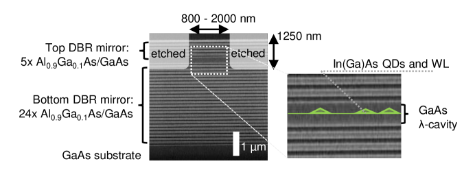
Sample structure. To fabricate our integrated single photon source waveguide device we use a semiconductor sample which contains self-assembled In(Ga)As QDs grown by the Stranski-Krastanow method at the center of a planar GaAs microcavity. The lower and upper cavity mirrors contain 24 and 5 pairs of Al0.9Ga0.1As/GaAs /4-layers, respectively, yielding a quality factor of 200. A -doping layer of Si donors with a surface density of roughly 1010 cm-2 was grown 10 nm below the layer of QDs to probabilistically dope them. The full layer structure is shown in Figure S1. In order to fabricate ridge waveguides, the top mirror layer along with GaAs cavity is etched down, forming the ridge with a width of 2 m or 0.8 m and a height of 1.25 m. Ridges have been defined by e-beam lithography and reactive ion etching followed by sidewalls passivation with 10 nm of SiN. After processing, the sample was cleaved perpendicularly to the WGs in order to get clear side access to the ridge facets.
Optical set-up. For all experiments, the sample is kept in a low-vibrations closed-cycle cryostat (attoDry800) at temperatures of 4.5 K. The cryostat is equipped with two optical windows allowing for access from both side and top of the sample. A spectroscopic setup consisting of two independent perpendicularly aligned optical paths is employed as shown schematically in Figure S2. QDs embedded into WG are excited from the top through a first microscope objective with NA = 0.4, while the emission signal is detected from a side facet of the WG with a second objective with NA = 0.4. Photoluminescence (PL) and resonance fluorescence signals are then passed through spatial filter and polarization optics. For light polarization control, a half-wave plate combined with a linear polarizer is used in both excitation and detection paths. The collected light is analyzed by a high-resolution monochromator equipped with a liquid nitrogen-cooled low-noise charge coupled device detector, featuring a spectral resolution of 20 eV. For non-resonant PL experiments, a 660 nm continuous wave laser is used while for resonance fluorescence investigations a tunable mode-locked Ti:Sapphire laser with repetition rate of 82 MHz and pulse width of around 2 ps is used.
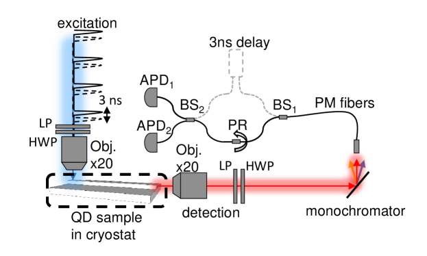
Auto-correlation and two-photon interference experiment details. In order to characterize investigated source purity and indistinguishability the resonance fluorescence signal is first passed through a monochromator to filter out (spectral width 50 pm/70 eV) broader laser profile and phonon sidebands, then it is coupled into a single-mode polarization maintaining fiber. Next, the light is introduced into a fiber-based unbalanced Mach-Zehnder interferometer for the two-photon interference measurements in the Hong-Ou-Mandel (HOM) configuration. To control the polarization of photons introduced into the second beam-splitter of the interferometer, a ceramic sleeve connector between two fiber facets is used allowing to align fast and slow light axis at the desired angle, and thus prepare photons in cross and parallel polarizations. For the auto-correlation measurements, one of the interferometer arms is blocked. Outputs ports are coupled to the two single-photon counting avalanche photo-detectors (APD) with a 350 ps temporal resolution. The photon correlation events are acquired by a multi-channel picosecond event timer. For the time-resolved experiments, a fast APD is used with a response time of 40 ps.
III Simulations details
Methods. We calculated an overall efficiency of a whole device by three-dimensional (3D) finite-difference-time-domain (FDTD) method. We used home-made FDTD software. The overall efficiency is defined as the probability to detect one photon from a QD through a waveguide into the collecting objective lens. Three efficiencies, coupling efficiency, output efficiency, collection efficiency, determine the overall efficiency. The QD emitter is modeled by a linearly polarized dipole source aligned along the transverse-electrically polarized waveguide mode. The dipole is placed at the center of the waveguide core. In the calculation, we assume a wavelength of 930 nm. The refractive indexes of GaAs and AlGaAs are set to 3.5652 and 3.0404, respectively. In order to represent infinite free space in the simulations, the uniaxial perfectly matched layer (UPML) was used as the absorbing boundary condition. On the other hand, to calculate the electric field distribution of the waveguide modes at a wavelength of 930 nm, a periodic boundary condition is used for the waveguide direction instead of the UPML boundary condition.
The coupling efficiency is defined as the ratio between the coupled photons into the waveguide mode and the emitted photons from a QD. The efficiency is estimated over the waveguide length of 40 m by 3D FDTD. On the other hand, the output efficiency, the ratio between the escaped photons from the waveguide output port into free space and the coupled waveguide photons, is directly calculated by integrating outgoing Poynting vectors out of the waveguide. The collection efficiency, the amount of the collecting photons by the objective lens (NA = 0.4) placed in front of the output port among the escaped photons from the waveguide, is obtained by calculating far-field distribution, showing the emission directions of photons.
QD-waveguide coupling efficiency. By performing three-dimensional FDTD calculations we investigated different DBR waveguide designs for maximized QD-waveguide coupling efficiency. Figure S3(a) shows simulations of the QD emitted light coupling efficiency into both WG arms vs width of the WG with fully etched bottom DBRs. Even though coupling efficiency itself is almost independent of the WG dimensions, the ratio of particular loss channels very strongly depends on the WG height. In case of small heights most if the light leaks into sides and bottom of the WG, while in the case of fully etched WGs, losses are almost explicitly related to the bottom substrate.
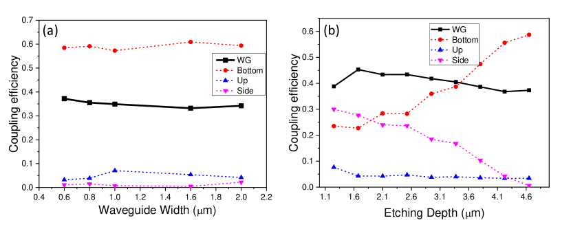
In Fig. S3(b) simulations of the QD emitted light coupling efficiency into both WG arms vs WG height for 0.6 m WG width are shown. A flat maximum of around 40-45% coupling efficiency can be observed for the 1.2-3.0 m WG heights. Maximal values of around 22% coupling efficiency into one WG arm in our case are defined mainly by the critical angle of the DBRs (19 deg), at which the reflectivity rapidly decreases. By integration of our DBR waveguides with low-refractive-index layers coupling efficiencies could be potentially further improved.
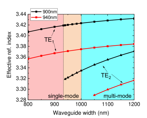
Single mode guiding in DBR waveguides. In Fig. S4 the effective refractive index vs WG width is shown, calculated for the fundamental (TE1) and first excited (TE2) TE mode of the 1.25 m height DBR waveguide at 900 and 940 nm wavelengths. As can be clearly seen, our DBR waveguides should operate in the single-mode regime for widths smaller than 0.930.01 m at 900 nm wavelengths and widths smaller than 1.000.05 m at a 940 nm wavelength. Taking into account simulations and fabrication inaccuracies, it should be possible to obtain single-mode operation for WGs with profile dimensions of 0.9x1.25 m under cut-off wavelengths of 900 nm.
Total output extraction efficiency. In order to check the properties of single photons generated on-chip, the fluorescence signal has to be out-coupled from the waveguide and introduced into the optical setup. We estimated that less than 5% (10%) of light initially coupled to the 2.0 m (0.8 m) wide MM (SM) WG is effectively collected by our microscope objective, which corresponds to the (i) waveguide transmission losses (29% loss for 1 mm travel), (ii) WG facet-air interface loss due to the reflection 81% (35%) and scattering 1% (15%), and finally (iii) mode mismatch between the WG and collection optics 51% (60%) loss. In total, around 0.88% (2.7%) of photons emitted from QD1 (QD2) should be collected into the first lens of the optical setup.
In this work, we focus on generating single photons with high mutual indistinguishability. It means that we cannot use all the photons generated by a QD since part of them are actually scattered by phonons making them distinguishable. This part of the QD emission spectrum (phonon sidebands) has to be removed, which forces us to use a spectral filter. We employ off-chip filtering with 100 eV width, which based on J. Iles-Smith et al. [Nat. Photonics 11, 521 (2017)] allows to achieve 99% indistinguishability and limits maximal obtainable efficiency to 83%.
Fraction of light coupled to each mode for 1.25 x 2.0 m MM waveguide. In the case of the DBR waveguide with 1.25 x 2.0 m profile dimensions, six modes are allowed for the guiding at 930 nm wavelength. Based on the FDTD calculations, if the central position of the QD would be assumed, most of the light coupled into the WG will be distributed between fundamental 1st mode (80.3%), 3rd mode (17.2%) and 5th mode (2.43%), while the 2nd, 4th and 6th will have negligible coupling ratio, due to the low overlap between centrally positioned QD dipole and WG mode distribution (0.0025%, 0.01%, 0.0004% respectively).
Purcell enhancement factor in DBR waveguides. In order to estimate the potential Purcell enhancement factor in case of our DBR waveguides, we performed FDTD simulations by putting a dipole emitter in the centre of our DBR waveguide and calculated the output power into the WG and compared it with the output power of an emitter in bulk. The spontaneous emission rate enhancement of the emitter in the WG in respect to the bulk is 0.94 and 0.96 for 1.25 x 2.0 m and 1.25 x 0.8 m WG profile dimensions, respectively.
IV Detail description of the two-photon interference histogram peaks
Peaks 1 and 5 of Fig.4(b) in the main text describe the process, where the first emitted photon is traveling through a shorter arm of the interferometer and second through longer one, which generates additional 3 ns delay and gives rise to bunching at 6 ns. Peaks labeled as 2 and 4 describes a process of the first and second photon traveling through the same arm in the interferometer, which is twice more probable than an earlier process and gives rise to the bunching at 3 ns. Peak 3 which describes the situation in which first emitted photon is delayed in the longer arm, and the second one travels through the shorter arm so that both photons superimpose into the second beam splitter. According to the above, for perfectly indistinguishable single photons the peak area ratio would be 1:2:0:2:1, in contrary to perfectly distinguishable single photons 1:2:2:2:1 ratio. The non-central peak clusters follow Poissonian statistics with the 1:2:6:2:1 ratio. In order to quantitatively evaluate the peak 3 area in respect to the neighboring peaks experimental data have been fitted with two-side exponential decay functions with a fixed area ratio of 1:3:6:3:1 and 1:2:X:2:1, for side and central peak clusters, respectively (red solid line). The zero delay peak relative area - X, and the Poissonian level were fitting parameter, while the decay time constant was fixed to value obtained in the time-resolved measurements. It needs to be noted here, that due to the 3 ns delay between the pulses, peaks positioned at 6 ns are imposed with 6 ns delayed peaks coming from the neighboring 12.2 ns delayed pulses, so that central cluster 2:2:0:2:2 ratio rather than 1:2:0:2:1 is visible. In this context inclusion of neighboring peaks into histogram analysis is needed.
V Two-photon interference histogram fitting and visibility extraction
In order to extract peaks areas of the two-photon interference histogram, experimental data have been fitted with the two-sided exponential decay function with a central peak intensity ratio of 1:2:X:2:1, where corresponds to the zero delay peak area, and 1:4:6:4:1 ratio for non-central peaks
| (1) |
where is corresponding to number 2 (4) central cluster peak amplitude of intensity, is a resonance fluorescence decay time, is a delay time between the pulse trains (3 ns) and is a repetition time of the laser (12.2 ns). The first line of the equation corresponds to the central cluster of peaks, while the second is the sum over non-central clusters. For the fitting procedure all values beside the and (fitting parameters), were fixed. The visibility has been calculated based on the central peak areas at zero delay and 3 ns delay and , which have been directly obtained from the fitting parameter
| (2) |
To take into account influence HOM interferometer imperfections limiting maximal obtainable experimentally visibilities, we corrected values according to
| (3) |
where is beam-splitter reflectivity/transmission ratio and is contrast of the HOM interferometer. The uncertainty of the value is calculated based on the fitting precision. We note that no corrections for the value nor the background were implemented.
| Waveguide | Emitter | Energy | |||||
|---|---|---|---|---|---|---|---|
| MM | QD1 | 1.3169 eV | 1.12 | 0.9897 | 0.949 | 0.9750.005 | 0.0090.002 |
| SM | QD2 | 1.3206 eV | 1.14 | 0.9915 | 0.923 | 0.9500.005 | 0.040.005 |
VI Laser contribution into resonance fluorescence spectra
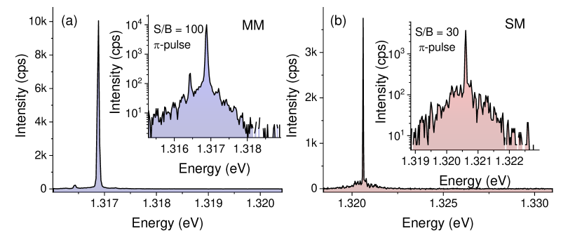
The excitation laser background intensity was tracked by observing a broader laser profile in resonance fluorescence spectra (Fig. S5) which is clearly visible in linear-log-scale (insets of Fig. S5). In case of QD1 much better signal-to-laser-background ratio was achieved for -pulse pumping than for QD2, which might be related to the QD emission energy located closer to the vertical cavity resonance (1.316 eV).
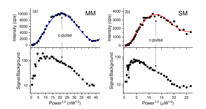
By utilizing both the intrinsic and polarization filtering we were able to obtain a signal-to-background (S/B) ratio in the range of 10-150 and 8-80 for QD1 and QD2, respectively, depending on the excitation power. In Figure S6(a) and (b) the resonance fluorescence peak intensity versus the square root of the incident power are shown. Based on the resonance fluorescence spectra, the signal-to-background ratio was estimated for a given set of powers and plotted in Fig. S6(c) and (d). The best S/B ratios were obtained for powers corresponding to the /2-pulse. Under -pulse excitation S/B ratio of around 100 and 30 for QD1 and QD2 have been obtained, respectively. We note here, that S/N ratio might to large extend limit single photon purity and indistinguishability values observable in HBT and HOM experiments.
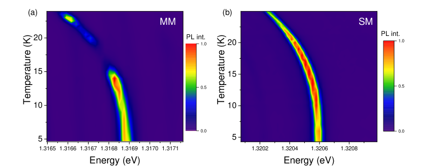
VII Temperature tuning of the QD emission
PL spectra for QD1 and QD2 exhibit intensity modulations, with a constant period of 200 eV and 370 eV corresponding to Fabry-Perot (FP) type oscillations between GaAs-air interfaces localized on the two ends of the waveguides. By tuning the QD emission energy with temperature along the FP resonances significant changes of the PL intensity can be observed as visible in Figures S7(a) and (b).
