High-temperature-grown buffer layer boosts electron mobility in epitaxial La-doped BaSnO3/SrZrO3 heterostructures
Abstract
By inserting a SrZrO3 buffer layer between the film and the substrate, we demonstrate a significant reduction of the threading dislocation density with an associated improvement of the electron mobility in La:BaSnO3 films. A room temperature mobility of 140 cm2 V is achieved for 25-nm-thick films without any post-growth treatment. The density of threading dislocations is only cm-2 for buffered films prepared on (110) TbScO3 substrates by pulsed laser deposition.
Transparent conducting oxides (TCOs) have attracted attention due to their unique properties and applications in electronic devices such as transparent displays and transistors.HOhta2003 ; WJLee2017 Recently, the transparent perovskite La:BaSnO3 has gained interest as a novel TCO due to its high mobility at room temperature (RT).HJKim2012-1 ; HJKim2012-2 Single crystals of La:BaSnO3 have been reported to have RT mobilities as high as 320 cm2 V (mobile carrier concentration cm-3).HJKim2012-2 At doping concentrations above cm-3, La:BaSnO3 has the second highest RT electron mobility among TCOs and other oxide single crystals HJKim2012-2 ; XLuo2012 ; HMIJaim2017 , exceeded only by CdO. ESachet2015 The high RT mobility in La:BaSnO3 has been attributed to the small electron-phonon interaction and small electron effective mass () arising from the large dispersion of the conduction band comprised of Sn 5s orbitals.APrakash2017 ; KKrishnaswamy2017 ; CANiedermeier2017 However, to fully explore the potential of La:BaSnO3, thin films with high mobilities are also required.
Recently, several efforts to achieve high carrier mobility in La:BaSnO3 films have been reported. JYue2018 ; KFujiwara2016 ; CPark2014 ; UKim2015 ; JShin2016 ; SArezoomandan2018 ; HPaik2017 ; ZWang2019 Nevertheless, as compared to bulk single crystals, even the best La:BaSnO3 epitaxial films show a reduced mobility ( cm2 V),HPaik2017 which specifically has been attributed to scattering from charge defects, such as threading dislocations (TDs)APrakash2017 ; HPaik2017 ; SRaghavana2016 ; HMun2013 and, more generally, to small carrier relaxation times.APrakash2017 ; KKrishnaswamy2017 TDs form for a large lattice mismatch between film and substrate, and extend perpendicularly through the films. The obvious solution to reduce TDs in La:BaSnO3 films is to use lattice-matched substrates, but unfortunately none exists. The substrate with the closest lattice match that is commercially available is PrScO3, mismatched by %.TMGesing2009 With such a high mismatch only thin commensurate layers of BaSnO3 can be grown; at a thickness of 32 nm the reported BaSnO3 films are almost fully relaxed and contain high densities of TDs.SRaghavana2016
To reduce the dislocation density in the La:BaSnO3 film, we explored the insertion of an undoped BaSnO3 buffer layer at the interface between the substrate (TbScO3) and the La:BaSnO3 film. As the thickness of the BaSnO3 layer increases, the TD density decreases as the threading component of dislocations annihilate each other, leaving behind a network of misfit dislocations. This method is known and has already led to the highest mobilities in BaSnO3 films to date; but even for thick buffer layers (330 nm), the remaining TD density is still cm-2. HPaik2017 Conceptually, growing this undoped BaSnO3 buffer layer at higher substrate temperatures should lower TD densities further, but due to the significant volatility of tin oxide at substrate temperatures above about 850°C, this is not a viable option.
In this work, we report on an alternative approach to significantly reduce the dislocation density and increase the mobility of La:BaSnO3 films. By inserting between the film and the substrate an insulating buffer layer of SrZrO3 grown at very high temperature, we greatly reduce the density of TDs. To avoid possible contamination, we first optimized the growth conditions of the films on (110) TbScO3 substrates thermally prepared in situ by directly heating the substrate with a CO2 laser. Without resorting to post-growth treatments, we achieve a significant reduction of the density of TDs from cm-2 to cm-2 and a maximum RT mobility of 140 cm2 V for La:BaSnO3 films prepared on a SrZrO3 buffer (grown at C). Extending prior reports, this RT mobility is obtained for films of small thickness (25 nm). It is the highest mobility for La:BaSnO3 films grown by PLD.
Epitaxial La:BaSnO3 films with a La-doping content of and a thickness of nm were grown on several (110) oriented TbScO3 single crystalline substrates ( mm3). All samples were grown by PLD ( nm) at a target-substrate distance of mm, using a CO2 laser substrate heating system. The La:BaSnO3 films were grown at C and J cm-2 at Hz in mbar of O2. Films were grown on either SrZrO3 or BaSnO3 buffer layers. The buffer layers were deposited at Hz to a thickness of nm. We chose SrZrO3 as a candidate because its lattice parameter value ( Å)EMete2003 ; AJSmith1960 is between that of La:BaSnO3 ( Å) and TbScO3 ( Å).WMa2018 Also, like TbScO3, SrZrO3 has a low vapor pressure and can therefore be grown at high temperatures. SrZrO3 layers were deposited at temperatures ranging from C to C with a laser fluence of J cm-2 at mbar of O2. The BaSnO3 buffer layers were grown at C with a fluence of J cm-2 at mbar of O2. Following Ref. HPaik2017 , BaSnO3 was chosen as it has roughly the same lattice parameter as La:BaSnO3.
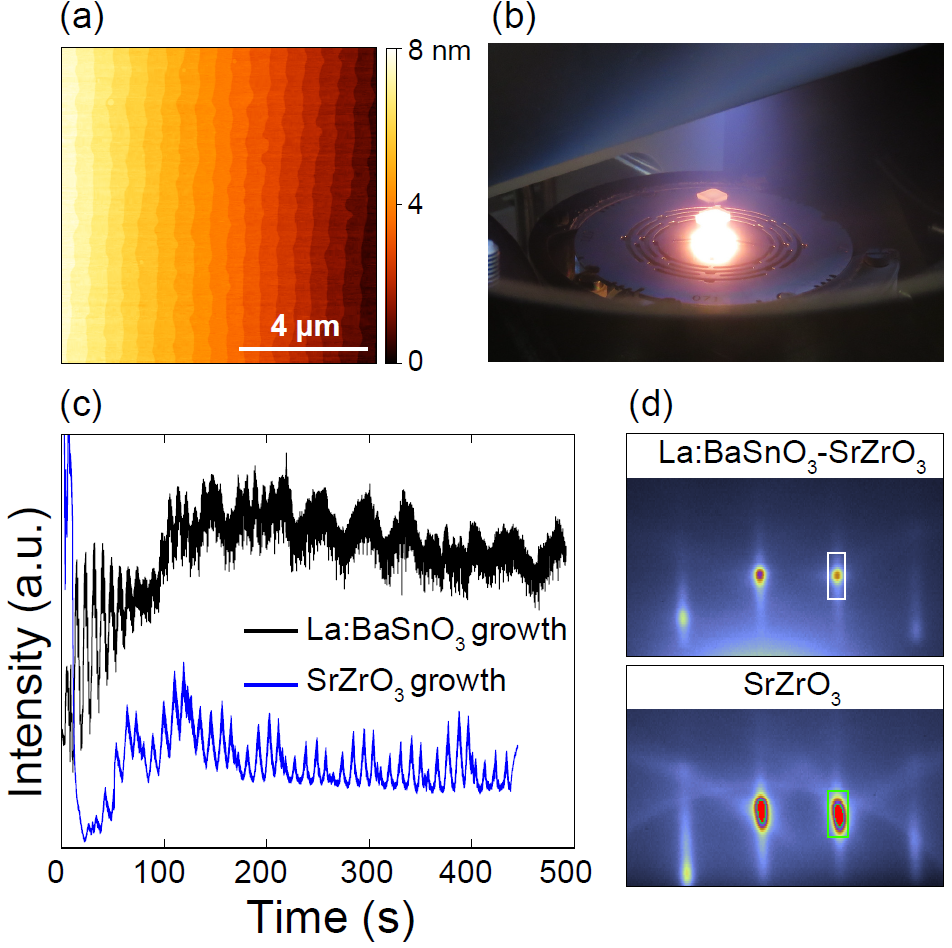
Prior to deposition, the TbScO3 substrates were in situ terminated at high temperature with the CO2 laser. Figure 1\textcolorblue(a) shows a typical atomic force microscopy (AFM) image of thermally prepared substrates heated at C for s. The substrate surface is smooth and well-ordered, with clear and uniform terraces. More details on the in situ thermal preparation of the substrates and related oxide surfaces are provided in Ref. MJager2019, . Figure 1\textcolorblue(b) shows a photograph of the growth chamber during the deposition of the SrZrO3 buffer layer at C.
The deposition of both the active layer (La:BaSnO3) and buffer layer (SrZrO3) were in situ monitored by reflection high-energy electron diffraction (RHEED) [Fig. 1\textcolorblue(c)]. The SrZrO3 layer was deposited at C. Immediately after the deposition, the sample was cooled to C at Ksec for the subsequent growth of the La:BaSnO3 film. We observe that the intensity of the RHEED oscillations remains the same throughout the deposition of the SrZrO3 layer. For the La:BaSnO3 film, the intensity drops after several monolayers and then stabilizes. The intensity drop suggests a relaxation in the film after a critical thickness has been reached (see Fig. S1 of the supplementary material). The RHEED data indicate that the SrZrO3 buffer layer and the La:BaSnO3 films are grown in a layer-by-layer mode with a smooth surface as also demonstrated by streaky RHEED patterns for both layers [see Fig. 1\textcolorblue(d))].
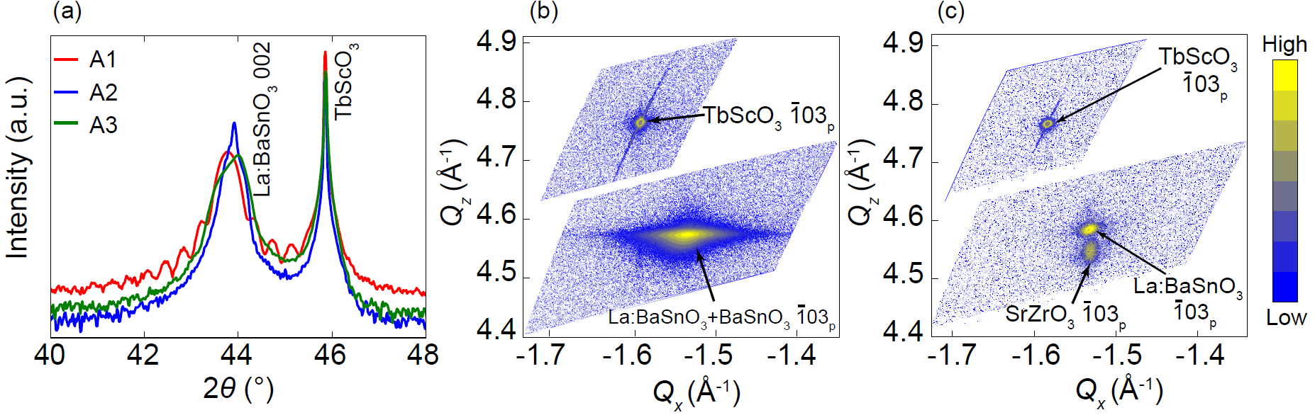
The crystalline quality and phase purity of the films were characterized by X-ray diffraction (XRD) using Cu Kα radiation. Figure 2\textcolorblue(a) shows the scans around the diffraction planes for the La:BaSnOTbScO3 (sample A1), La:BaSnOBaSnOTbScO3 (sample A2) and La:BaSnOSrZrOTbScO3 (sample A3) films. Laue thickness fringes and phase-pure La:BaSnO3 peaks are observed, indicating smooth growth and high crystallinity [Fig. 2\textcolorblue(a), see also Fig. S2 of the supplementary material]. The film thicknesses were extracted from the Laue thickness fringes and the Kiessig fringes observed by XRD. The extracted out-of-plane lattice parameters are Å, Å and Å for samples A1, A2 and A3. These values are consistent with the out-of-plane lattice constants reported previously for La:BaSnO3 filmsWJLee2016 ; HMun2013 and are close to the bulk lattice parameter ( Å) of polycrystalline La:BaSnO3.THuang1995 ; CANiedermeier2016 Figures 2\textcolorblue(b) and 2\textcolorblue(c) show reciprocal space maps (RSM) around the asymmetric () reflection peaks of the films (samples A2 and A3) and the substrate. The in-plane and out-of-plane lattice constants of the film in sample A2 are Å and Å, respectively, indicating that the film is almost completely relaxed. The relatively small deviation of the lattice constants is attributed to the large lattice mismatch () between BaSnO3 and the TbScO3 [Fig. 2\textcolorblue(b)]. The broadening of the film peak indicates the presence of a large density of dislocations. For sample A3, the extracted in-plane and out-of-plane lattice constants are Å, Å, indicating that the film is fully strained in the a direction () and partially relaxed in the c direction. From the XRD data (see Fig. S3 of the supplementary material) of a control sample of SrZrO3 grown at C (in the same growth conditions as the buffer layer in sample A3), in-plane and out-of-plane lattice constants of Å and Å are obtained, indicating that the buffer layer is almost fully strained to the substrate ( Å), suggesting a small number of dislocations in the film A3 as discussed below.
Resistivity (), electron mobility () and carrier concentration (n) were characterized in a physical property measurement system (PPMS) in a van der Pauw geometry by wire bonding aluminum wires to the samples’ corners. An excitation current of A was used. Using the procedure discussed in Refs. PNgabonziza2016 ; PNgabonziza2018 , the carrier concentration was calculated as , where is the measured Hall coefficient; and the electron mobility was extracted from , where was determined by the Van der Pauw method. Figure 3\textcolorblue(a) presents the temperature dependence of the resistivity at zero magnetic field for the samples A1, A2 and A3. All films exhibit metallic behavior over the entire temperature range, consistent with previous reports on La:BaSnO3.HJKim2012-1 ; HJKim2012-2 The temperature dependence of the carrier density shows the bahavior of a degenerate semiconductor. HJKim2012-1 The concentration of the negatively charged carriers is temperature independent at high temperatures, but starts to decrease below 50 K following the freeze out at the La+3 ions [Fig. 3\textcolorblue(b)]. PVWadekar2014 The temperature dependence of the electron mobility is presented in Fig. 3\textcolorblue(c). For all three samples, increases down to the lowest temperature ( K), contrary to previous studies which reported a saturation below 50 K.SRaghavana2016 ; HPaik2017 This behavior suggests a significant reduction of phonon scattering for these films at low temperatures.
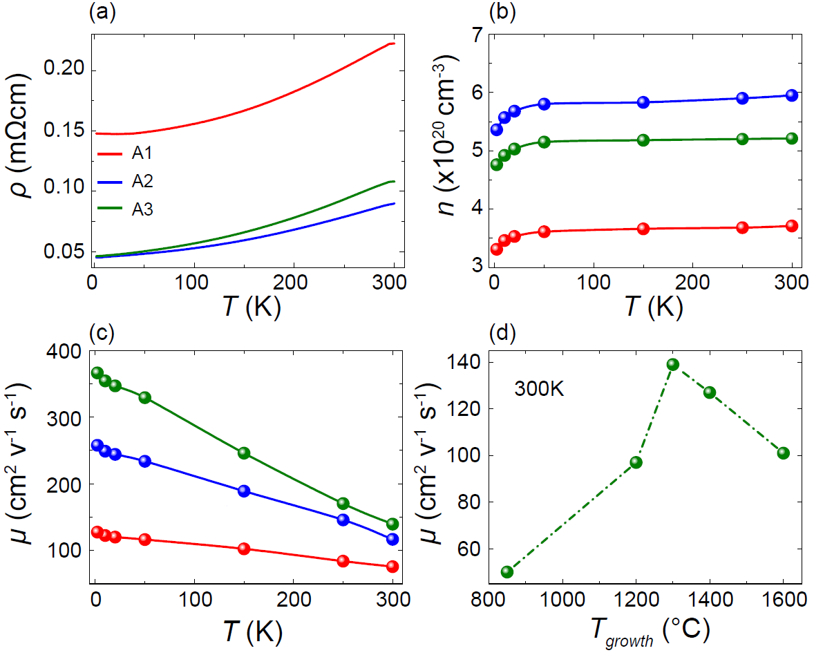
For the sample directly grown on the substrate (A1), a mobility of 76 cm2 V (RT) was measured. In the sample with the BaSnO3 buffer layer (A2), the RT is improved to 117 cm2 V, but apparently still limited by the high density of TDs, as discussed below. To reduce the density of TDs, we switched to SrZrO3 buffer layers. Several La:BaSnOSrZrO3 heterostructures were prepared by varying the growth temperatures of the SrZrO3 layer from C to C, while keeping the other growth parameters constant. We find C as the optimal growth temperature of the SrZrO3 buffer layer to achieve high mobility in the La:BaSnO3 layers [Fig. 3\textcolorblue(d)]. Above C the buffer layers start to become more non-stoichiometric, i.e., the ratio of Sr:Zr deviating from 1 in SrZrO3 due to the volatility of constituents Engel-Herbert2013 (see Fig. S3(d) in supplemental materials). This results in an enhanced defect density (e.g. shear defects and/or point defects arising from nonstoichiometry HPaik2017 ), limiting the mobility of the La:BaSnO3 layers deposited on buffer layers grown at temperatures above C. The sample A3 prepared on a buffer layer grown at C has the highest mobility cm2 V (RT) and cm2 V ( K) [Fig. 3\textcolorblue(c)]. For PLD grown La:BaSnO3 thin films, this RT is higher than the previous record ( cm2 V) achieved without post-growth treatment on BaSnO3 substrates;WJLee2016 and higher than reported enhanced mobility ( cm2 V) after post-annealing processes in H2 forming gas at C on SrTiO3.DYoon2018
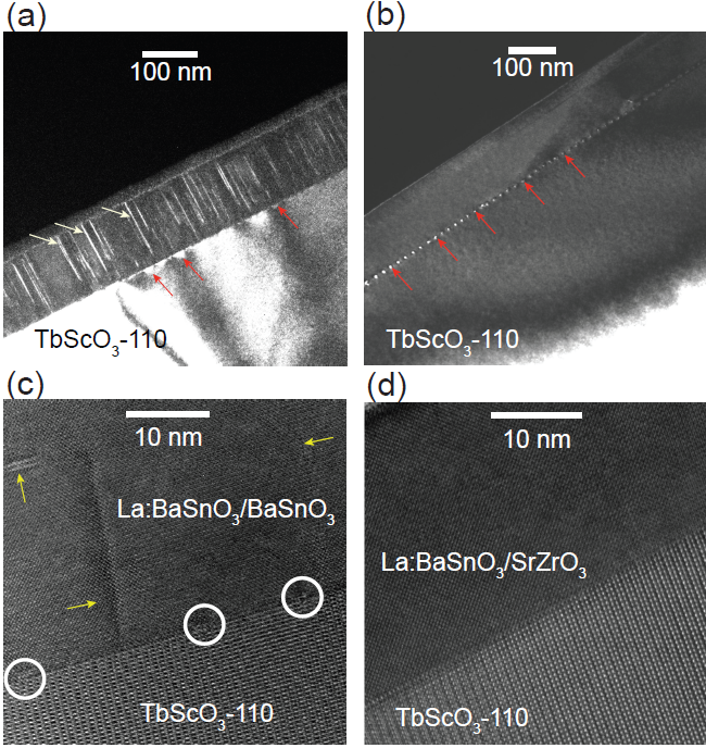
To further investigate the role of TDs that act as scattering centers and trap electrons,APrakash2017 ; HMun2013 ; JShin2016 ; SYu2016 we studied the defect structure of the samples A2 and A3 using cross-sectional transmission electron microscopy (TEM). Figures 4\textcolorblue(a) and 4\textcolorblue(b) present the weak-beam dark-field TEM (WB-DFTEM) images of the entire film thickness for the samples A2 and A3, respectively. For both samples misfit dislocations are visible along the interface as bright dots, indicated in figures 4\textcolorblue(a) and 4\textcolorblue(b) by red arrows. To accommodate the large lattice mismatch between the substrate and the film, these misfit dislocations generate edge-type defects, which extend vertically through the film (bright contrast indicated by white arrows in Fig. 4\textcolorblue(a)). For a TEM specimen of nm thick, the extracted density of TDs in sample A2 was cm-2. This density of TDs is in agreement with previous reports on La:BaSnO3 films prepared on DyScO3HPaik2017 and SrTiO3HMun2013 substrates. Interestingly, TDs were barely observed in the highest mobility sample A3 as shown in the WB-DFTEM image in Fig. 4\textcolorblue(b). Even for a TEM specimen of nm thick, the TDs density was cm-2 which is two orders of magnitude lower than the one in the sample A2 and previously reported TD densities for La:BaSnO3 films.HPaik2017 ; HMun2013 Figures 4\textcolorblue(c) and 4\textcolorblue(d) depict the high resolution TEM images of samples A2 and A3, respectively. A fully relaxed interface between the TbScO3 substrate and the BaSnO3 layer is seen in sample A2 as indicated by white circles. Additional structural defects such as stacking faults are also visible in the film [see yellow arrows in Fig. 4\textcolorblue(c)]. On the other hand, a strained interface is seen in sample A3 with no apparent structural defects [Fig. 4\textcolorblue(d)].
The low density of TDs in sample A3 is attributed to the high temperature used for the SrZrO3 buffer layer growth. One of the effective ways of minimizing the TDs density is to enhance the motion and reaction of TDs by high thermal stress. This method was demonstrated to be efficient in epitaxial semiconductor GaAs films on Si substrates.YTakagi1994 ; DDeppe1988 At high temperatures, the velocity of the dislocations glide motion and the concentration of vacancies that support the climb motion of the dislocations are exponentially enhanced.IYonenaga1987 Thus, the observed significant reduction of the TDs density in sample A3 is attributed to the enhancement of the glide and climb motion at high temperatures. Stress that increases the glide motion originates from the difference in the thermal expansion coefficients of between SrZrO3 and TbScO3RUecker2008 ; DdeLigny1996 and also possible grown-in strain in the SrZrO3 layer. The latter is supported by the fact that SrZrO3 undergoes a phase transition from tetragonal to cubic at high temperature,DdeLigny1996 indicating epitaxial strain at the interface during cool down, yielding a reduction of the lattice mismatch. Our results suggest that the high temperature grown SrZrO3 epilayer deposited not only on TbScO3 but also on other oxide substrates (e.g. SrTiO3, DyScO3, MgO) can be utilized as a template for subsequent growth of high mobility La:BaSnO3 films with fewer TDs.
Although we have demonstrated that by inserting a high-temperature grown SrZrO3 buffer layer between the film and the substrate the density of TDs significantly reduces with an associated improvement of the electron mobility in La:BaSnO3 films, we point to several observations. Normally, scattering by TDs not only diminishes the electron mobility, but also reduces the number of free charge carriers HMun2013 . However, we observe that the carrier density of sample A2 (with the high density of TDs) is higher than sample A3 (with a low TD density) [Fig. 3\textcolorblue(b)]. Given that the active layer in our samples is thin (25 nm), the lower number of free charge carriers in sample A3 suggests that not only TDs are trapping electrons, but that also effects such as surface scattering or interface traps are lowering the density of mobile carriers. For the sample A2, these contributions are expected to be less pronounced as the buffer layer (BaSnO3) and the active layer consist of the same materials.
In summary, we explore the possible use of buffer layers grown at very high temperatures for the reduction of TDs and improvement of electron mobility in epitaxial La-doped BaSnOSrZrO3 heterostructures grown on (110) TbScO3 substrates. For La:BaSnO3 films prepared on a SrZrO3 buffer layer grown at C a RT mobility of 140 cm2 V has been achieved, together with a reduction of the density of TDs to cm-2, all without post-growth sample treatment.
With the insertion of a high temperature grown buffer layer between the La:BaSnO3 film and the TbScO3 substrate, the mobility has been doubled, which opens a new road towards high mobilities in La:BaSnO3 based electronic devices.
We acknowledge valuable discussions with Darrell G. Schlom and Hans Boschker, and thank Helga Hoier and Marion Hagel for technical assistance.
References
- (1) H. Ohta, K. Nomura, H. Hiramatsu, K. Ueda, T. Kamiya, M. Hirano, H. Hosono, Solid State Electron. 47, 2261 (2003).
- (2) W.-J. Lee, H. J. Kim, J. Kang, D. H. Jang, T. H. Kim, J. H. Lee, and K. H. Kim, Annu. Rev. Mater. Res. 47, 391 (2017) and references therein.
- (3) H. J. Kim, U. Kim, T. H. Kim, J. Kim, H. M. Kim, B-G. Jeon, W-J. Lee, H. S. Mun, K. T. Hong, J. Yu, K. Char, and K. H. Kim, Phys. Rev. B 86, 165205 (2012).
- (4) H. J. Kim, U. Kim, H. M. Kim, T. H. Kim, H. S. Mun, B-G. Jeon, K. T. Hong, W-J. Lee, C. Ju, K. H. Kim, and K. Char, Appl. Phys. Express. 5, 061102 (2012).
- (5) X. Luo, Y. S. Oh, A. Sirenko, P. Gao, T. A. Tyson, K. Char, and S. W. Cheong, Appl. Phys. Lett. 100, 172112 (2012).
- (6) H. M. I. Jaim, S. Lee, X. H. Zhang, and I. Takeuchi, Appl. Phys. Lett. 111, 172102 (2017).
- (7) E. Sachet, C. T. Shelton, J. S. Harris, B. E. Gaddy, D. L. Irving, S. Curtarolo, B. F. Donovan, P. E. Hopkins, P. A. Sharma, A. L. Sharma, et al., Nat. Mater. 14, 414 (2015).
- (8) A. Prakash, P. Xu, A. Faghaninia, S. Shukla, J. W. Ager, C. S. Lo and B. Jalan, Nat. Commun. 8, 15167 (2017).
- (9) K. Krishnaswamy, B. Himmetoglu, Y. Kang, A. Janotti, and C. G. Van de Walle, Phys. Rev. B 95, 205202 (2017).
- (10) C. A. Niedermeier, S. Rhode, K. Ide, H. Hiramatsu, H. Hosono, T. Kamiya, and M. A. Moram, Phys. Rev. B 95, 161202(R) (2017).
- (11) J. Yue, A. Prakash, M. C. Robbins, S. J. Koester, and B. Jalan, ACS Appl. Mater. Interfaces 10, 21061 (2018).
- (12) K. Fujiwara, K. Nishihara, J. Shiogai, and A. Tsukazaki, Appl. Phys. Lett. 110, 203503 (2017).
- (13) J. Shin, Y. M. Kim, Y. Kim, C. Park, and K. Char, Appl. Phys. Lett. 109, 262102 (2016).
- (14) C. Park, U. Kim, C. Jong Ju, J. S. Park, Y. M. Kim, and K. Char, Appl. Phys. Lett. 105, 203503 (2014).
- (15) U. Kim, C. Park, T. Ha, Y. M. Kim, N. Kim, C Ju, J. Park, J. Yu, J. H. Kim, and K. Char, APL Mater. 3, 036101 (2015).
- (16) S. Arezoomandan, A. Prakash, A. Chanana, J. Yue, J. Mao, S. Blair, A. Nahata, B. Jalan, and B. Sensale-Rodriguez, Sci. Rep. 8, 3577 (2018).
- (17) Z. Wang, H. Paik, Z. Chen, D. A. Muller, and D. G. Schlom, APL Mater. 7, 022520 (2019).
- (18) H. Paik, Z. Chen, E. Lochocki, A. Seidner H, A. Verma, N. Tanen, J. Park, M. Uchida, S. Shang, B.-C. Zhou, M. Brützam, R. Uecker, Z.-K. Liu, D. Jena, K. M. Shen, D. A. Muller, and D. G. Schlom, APL Mater. 5, 116107 (2017).
- (19) S. Raghavana, T. Schumanna, H. Kim, J. Y. Zhang, T. A. Cain, and S. Stemmer, APL Mater. 4, 016106 (2016).
- (20) H. Mun, U.Kim, H. M.Kim, C. Park, T. H. Kim, H. J. Kim, K. H. Kim, and K. Char, Appl. Phys. Lett. 102, 252105 (2013).
- (21) T. M. Gesing, R. Uecker, and J. C. Buhl, Kristallogr. NCS 224, 365 (2009).
- (22) E. Mete, R. Shaltaf, and Ş. Ellialtıoğlu, Phys. Rev. B 68, 035119 (2003).
- (23) A. J. Smith and A. J. E. Welch, Acta Crystallogr. 13, 653 (1960).
- (24) W. Ma, X. Li, X. Meng, Y. Xue, Y. Bai, W. Chen, and H. Dong, J. Therm. Spray Tech. 27, 1056 (2018).
- (25) M. Jäger, G. Laskin, P. Ngabonziza, W. Voesch, P. Wittlich, J. Mannhart, and W. Braun, In situ thermal preparation of oxide surfaces (in preparation, 2019).
- (26) W. J. Lee, H. J. Kim, E. Sohn, T. H. Kim, J. Y. Park, W. Park, H. Jeong, T. Lee, J. H. Kim, K. Y. Choi, and K. H. Kim, Appl. Phys. Lett. 108, 082105 (2016).
- (27) T. Huang, T. Nakamura, M. Itoh, Y. Inaguma, and O. Ishiyama, J. Mater. Sci. 30, 1556 (1995).
- (28) C. A. Niedermeier, S. Rhode, S. Fearn, K. Ide, M. A. Moram, H. Hiramatsu, H. Hosono, and T. Kamiya, Appl. Phys. Lett. 108, 172101 (2016).
- (29) P. Ngabonziza, M. P. Stehno, H. Myoren, V. A. Neumann, G. Koster, and A. Brinkman, Adv. Electron. Mater. 2, 1600157 (2016).
- (30) P. Ngabonziza, Y. Wang, and A. Brinkman, Phys. Rev. Mater. 2, 044204 (2018).
- (31) P. V. Wadekar, J. Alaria, M. OŚullivan, N. L. O. Flack, T. D. Manning, L. J. Phillips, K. Durose, O. Lozano, S. Lucas, J. B. Claridge, and M. J. Rosseinsky, Appl. Phys. Lett. 105, 052104 (2014).
- (32) Roman Engel-Herbert, Molecular beam epitaxy of complex oxides (Book chapter in Molecular Beam Epitaxy), edited by Mohamed Henini, Elsevier, Amsterdam, Pages: 417-449 (2013).
- (33) D. Yoon, S. Yu, and J. Son, NPG Asia Mater. 10, 363 (2018).
- (34) S. Yu, D. Yoon, and J. Son, Appl. Phys. Lett. 108, 262101 (2016).
- (35) D. Deppe, N. Holonyak Jr, K. Hsieh, D. Nam, W. Plano, R. Matyi, and H. Shichijo, Appl. Phys. Lett. 52, 1812 (1988).
- (36) Y. Takagi, H. Yonezu, Y. Hachiya, and K. Pak, Jpn. J. Appl. Phys. 33, 3368 (1994).
- (37) I. Yonenaga and K. Sumino, J. Appl. Phys. 62, 1212 (1987).
- (38) R. Uecker, B. Velickov, D. Klimm, R. Bertram, M. Bernhagen, M. Rabe, M. Albrecht, R. Fornari, and D. Schlom, J. Cryst. Growth 310, 2649 (2008).
- (39) D. de Ligny and P. Richet, Phys. Rev. B 53, 3013 (1996).
*Supplementary information:
High-temperature-grown buffer layer boosts electron mobility in epitaxial La-doped BaSnO3/SrZrO3 heterostructures
Arnaud P. Nono Tchiomo1,2, Wolfgang Braun1, Bryan P. Doyle2, Wilfried Sigle1, Peter van Aken1, Jochen Mannhart1, and Prosper Ngabonziza1,2
1)Max Planck Institute for Solid State Research, Heisenbergstr. 1, 70569
Stuttgart, Germany
2)Department of Physics, University of Johannesburg, P.O. Box 524 Auckland Park 2006,
Johannesburg, South Africa
Analysis of RHEED intensity oscillations
Reflection high-energy electron diffraction (RHEED) data were acquired using the Safire data acquisition software. The RHEED gun was a differentially pumped Staib system operated at 30 keV. To fit the RHEED raw data from our samples, we followed the procedure for the analysis of the RHEED intensity oscillations presented in Refs. Braun1 ; Braun2 . We show below RHEED data of the La:BaSnO3 active layer and SrZrO3 buffer layer for the highest mobility sample A3 discussed in the main text.
![[Uncaptioned image]](/html/1903.11645/assets/1.png)
Figure S1: RHEED intensity oscillations during the growth of the sample A3 discussed in the main text. (a) Intensity oscillations during the growth of SrZrO3 buffer layer (red curve) together with a best fit to the raw data (cyan curve). The bottom green curve was obtained by using an algorithm for RHEED data analysis from Ref. [\textcolorblue1] and the transformed data were then fitted by a sine function (black curve). (b) The same analysis was performed on the 25-nm-thick La:BaSnO3 grown on top of the SrZrO3 buffer layer.
X-ray diffraction measurements
We present here additional x-ray diffraction (XRD) measurements over a wider region for the samples A1 (La:BaSnO3/TbScO3), A2 (La:BaSnO3/BaSnO3/TbScO3) with the buffer layer grown at 850C and A3 (La:BaSnO3/SrZrO3/TbScO3) with the buffer layer grown at 1300C. Data from these samples are discussed in the main text. Only phase-pure 00l peaks from the film are observed, underlining the crystalline quality of the samples.
![[Uncaptioned image]](/html/1903.11645/assets/2.png)
Figure S2: XRD measurements. scans over a wider region for the samples (a) A1, (b) A2 and (c) A3 showing only phase-pure 00l peaks from the samples.
Characterization of SrZrO3 buffer layer
XRD and atomic force microscopy (AFM) data for a control sample of SrZrO3 grown at 1300C are presented. The sample was prepared in the same growth conditions as the buffer layer in the sample A3 discussed in the main text. The lattice mismatch between SrZrO3 and TbScO3 from this control sample grown at C was reduced from to . As suggested by the SrO partial pressure vs. temperature diagram (see Fig. \textcolorblueS3 (d)), the stoichiometry of the SrZrO3 buffer layer deteriorates at very high growth temperatures (above C) due to the volatility of SrO.
![[Uncaptioned image]](/html/1903.11645/assets/3.png)
Figure S3: Characterization of the SrZrO3 buffer layer. (a) scan over a wider region for a 100 nm thick SrZrO3 buffer layer grown at 1300C on a TbScO3 substrate. Only the phase-pure 00l peaks from the SrZrO3 film are observed. (b) Reciprocal space map and (c) AFM image of the same SrZrO3 film. (d) SrO phase diagram (adapted from Ref. Engel-Herbert2013 ).
| SrZrO3 growth | ||||
| temperature | In-plane lattice constant | Out-of-plane lattice constant | Carrier density at 300 K | Mobility at 300 K |
| La:BaSnO3 | La:BaSnO3 | |||
| (∘C) | a (Å) | c (Å) | (cm-3) | (cm2 V-1 s-1) |
| 850 | 4.09 | 4.136 | 50 | |
| 1200 | 4.07 | 4.14 | 97.4 | |
| 1300 | 4.103 | 4.113 | 140 | |
| 1300 | 4.103 | 4.113 | 136.2 | |
| 1400 | 4.10 | 4.115 | 127 | |
| 1600 | 4.06 | 4.142 | 100.8 |
References
- (1) Wolfgang Braun, J. Cryst. Growth 477, 50 (2017).
- (2) Wolfgang Braun, J. Cryst. Growth 477, 34 (2017).
- (3) Roman Engel-Herbert, Molecular beam epitaxy of complex oxides (Book chapter in Molecular Beam Epitaxy), edited by Mohamed Henini, Elsevier, Amsterdam, Pages: 417-449 (2013).