Grooved Dayem nanobridges as building blocks of high-performance YBa2Cu3O7-δ SQUID magnetometers
Abstract
We present noise measurements performed on a YBa2Cu3O7-δ nanoscale weak-link-based magnetometer consisting of a Superconducting QUantum Interference Device (SQUID) galvanically coupled to a mm2 pick-up loop, reaching white flux noise levels and magnetic noise levels as low as and fT/ at K, respectively. The low noise is achieved by introducing Grooved Dayem Bridges (GDBs), a new concept of weak-link. A fabrication technique has been developed for the realization of nanoscale grooved bridges, which substitutes standard Dayem bridge weak links. The introduction of these novel key blocks reduces the parasitic inductance of the weak links and increases the differential resistance of the SQUIDs. This greatly improves the device performance, thus resulting in a reduction of the white noise.
Keywords: High-Tc, SQUID, magnetometer, YBCO, Grooved Dayem Bridge.
Charmers University of Technology]Quantum Device Physics Laboratory, Department of Microtechnology and Nanoscience, Chalmers University of Technology, SE-41296 Göteborg, Sweden Charmers University of Technology]Quantum Device Physics Laboratory, Department of Microtechnology and Nanoscience, Chalmers University of Technology, SE-41296 Göteborg, Sweden Charmers University of Technology]Quantum Device Physics Laboratory, Department of Microtechnology and Nanoscience, Chalmers University of Technology, SE-41296 Göteborg, Sweden Charmers University of Technology]Quantum Device Physics Laboratory, Department of Microtechnology and Nanoscience, Chalmers University of Technology, SE-41296 Göteborg, Sweden \alsoaffiliation[Second University] Dipartimento di Fisica, Politecnico di Milano, Piazza Leonardo da Vinci 32, I-20133 Milano, Italy Charmers University of Technology]Quantum Device Physics Laboratory, Department of Microtechnology and Nanoscience, Chalmers University of Technology, SE-41296 Göteborg, Sweden Charmers University of Technology]Quantum Device Physics Laboratory, Department of Microtechnology and Nanoscience, Chalmers University of Technology, SE-41296 Göteborg, Sweden Charmers University of Technology]Quantum Device Physics Laboratory, Department of Microtechnology and Nanoscience, Chalmers University of Technology, SE-41296 Göteborg, Sweden Charmers University of Technology]Quantum Device Physics Laboratory, Department of Microtechnology and Nanoscience, Chalmers University of Technology, SE-41296 Göteborg, Sweden
Superconducting QUantum Interference Devices (SQUIDs) are among the most sensitive magnetometers available today, making them one of the most prominent devices for various applications of superconducting materials. Since their introduction, SQUIDs have been used in several technological applications, e.g. geophysical surveys 1, medical diagnostic (MCG and MEG) 2, 3, 4 and scanning SQUID microscopy 5.
While the basic operation of SQUIDs is well established 6, great effort is still invested in the improvement of their performance. In this respect, the recent technological advances in nano-fabrication enabled the realization of nanoSQUIDs with white flux noise levels well below 7, 8, 9, 10, 11, 12, 13, 14, opening the way to single spin detection, a milestone of experimental physics 15, 16.
SQUIDs made of High critical Temperature Superconductors (HTS) have a much wider temperature range of operation (from mK to above 77 K) compared to their Low critical Temperature Superconductor (LTS) counterparts, greatly simplifying their practical applications. HTS SQUID magnetometers are promising candidates for future on-scalp magnetoencephalography systems 17, 18, 19, 20. Tremendous efforts have been devoted to achieve high quality HTS Josephson Junctions (JJs), the key ingredient of a SQUID, during the last few decades. This has proven to be challenging for cuprate HTS materials, due to the chemical instability, the small superconducting coherence length ( nm in the ab-planes) and the ceramic and granular nature of these materials. Nevertheless, different JJ fabrication techniques have been successfully developed for HTS SQUIDs so far. For example, high sensitivity HTS SQUIDs have been realized using grain boundary based JJs, by epitaxial growth of HTS films on bicrystal or step edge substrates 21, 22, 20, 23, 10, 24, 25.
HTS nanoSQUIDs, realized with Dayem bridges, have also shown low magnetic flux noise properties, in combination with a simplified fabrication procedure 8, 11, 12. However, the rather large parasitic inductance of Dayem bridges limits their implementation in SQUID magnetometers at K 4. Another approach to fabricate HTS weak links is by high energy ion irradiation (30-200 keV) of predefined wide YBCO bridges through a mask 26 or by direct irradiation using a He focused ion beam (FIB) 27. This resulted in high quality low noise SQUID devices at 4 K and 50 K28, 29. RF-SQUIDs working at 77 K and above have been realized showing a white flux noise level of 30, which is more than one order of magnitude higher than values obtained in state of the art dc-SQUIDs 20, 23, 31, 22, 25. DC-SQUID devices operational at 77 K have been realized by oxygen ion irradiation, however no frequency dependent noise data have been reported 32.
In this work we present a novel fabrication process of a HTS weak link: the nanoscale Grooved Dayem Bridge (GDB), which exhibits Josephson Junction-like behavior. Here, the layout of the bridge and the weak link inside the bridge are realized during one single lithography process on a YBa2Cu3O7-δ (YBCO) film grown on a single crystal substrate. Moreover, such weak links can be defined anywhere on the chip and freely oriented within the film plane. This approach has clear advantages compared to bicrystal HTS junctions, where the junctions are located at the grain boundary line, and to step edge junctions, which involve more than one lithography step 33 and several epitaxial thin film depositions 31.
We have used YBCO GDBs as novel, alternative building nanoscale blocks in HTS SQUID magnetometers, which have been characterized via transport and noise measurements at T K. In particular, these devices exhibit large voltage modulations (V) and low values of white magnetic flux noise, (compared to the lowest reported flux noise at K 25), and corresponding magnetic field noise, fT, at K. Therefore, GDB based SQUIDs combine the nanofabrication advantages and the device reproducibility, which are typical of Dayem bridges, with the performances, e.g. the magnetic sensitivity, of state-of-the-art SQUIDs based on grain boundary JJs.
A nm thick film of YBCO is deposited by Pulsed Laser Deposition (PLD) onto a (001) SrTiO3 substrate with lateral dimensions of mm2. On top of the YBCO film, a mask layer of amorphous hard carbon with thickness nm is deposited by PLD and defined by e-beam lithography (EBL). The device is finally patterned by gentle low energy (300 eV) Ar ion milling, as described in previous works 34, 35. The detailed ion milling parameters are summarized in the supporting information, table S1. This fabrication procedure has been shown to result in YBCO nanowires with pristine bulk-like properties 34, 35, 36, 37. Here, in order to fabricate the Grooved Dayem Bridges, we start from this fabrication and take advantage of a reduced etching rate of the ion milling in specifically designed areas of the sample. To achieve this, the standard mask design for the Dayem bridge is modified, opening a gap along the full width, as shown in Figure 1(a).
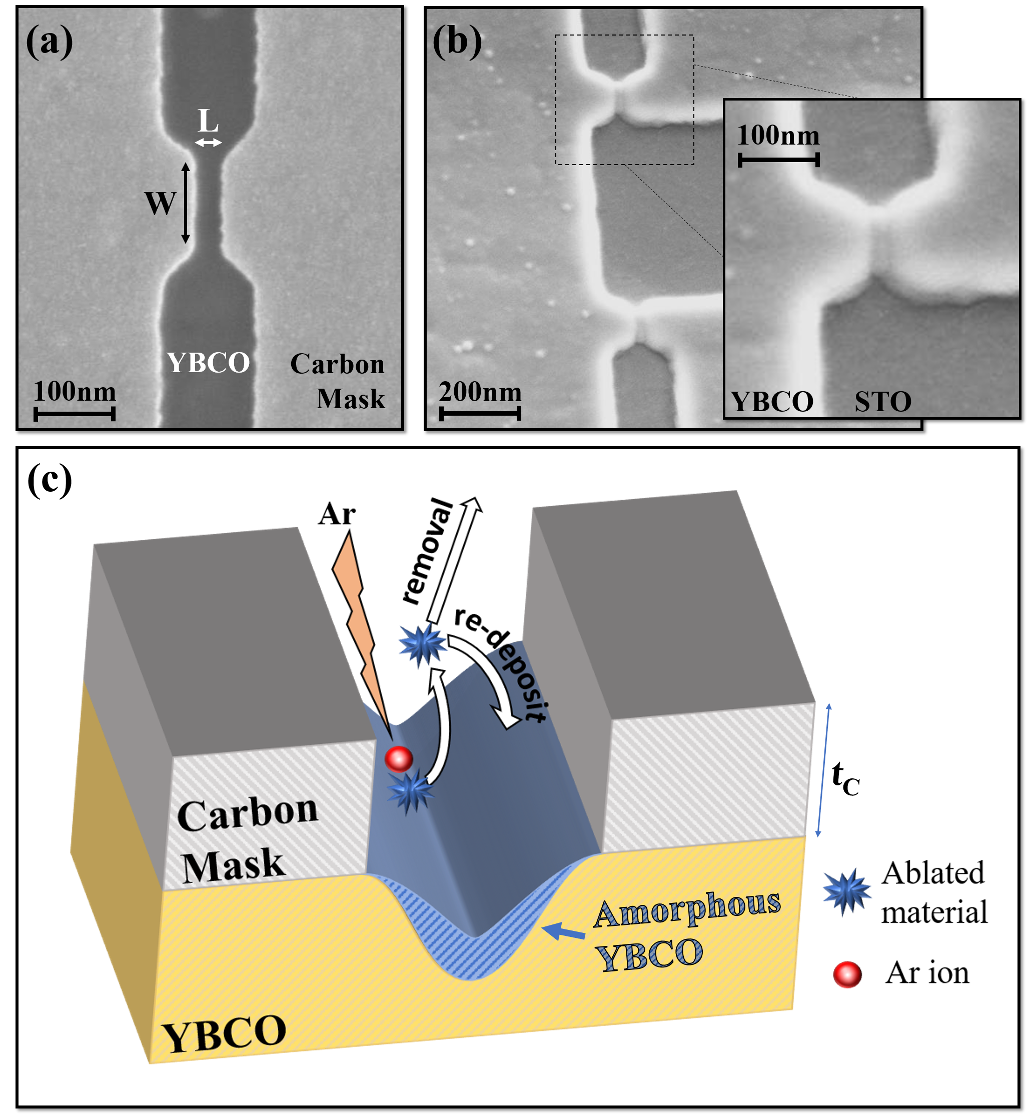
The width and length of the gap define the geometrical dimensions of the final GDB and can be varied to achieve different values of critical current . For aspect ratios of the gap in the carbon mask , the etching rate of YBCO during the Ar ion milling inside the gap is strongly reduced compared to the rest of the sample. This is the result of partial re-deposition of the YBCO ablated by the Ar ions, which cannot be removed from the gap and forms an amorphous layer of YBCO 38 (see Fig.1(c)). Since the etching rate inside the gap is reduced, the ion milling process required to remove nm of YBCO far away from the carbon mask edges results only in a slight thinning of the YBCO inside the gap, leaving a grooved bridge with thickness less than nm. The final result obtained for a SQUID after the final ion milling is shown in Figure 1(b).
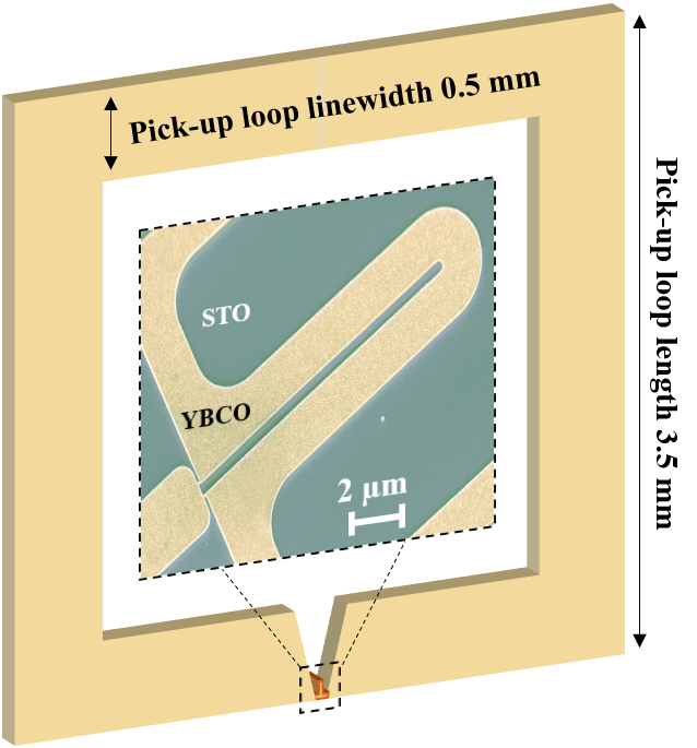
Up to 16 GDB-SQUIDs can be fabricated on the same pick-up loop. The widths of the GDBs are nm and the gap length in the bridge mask nm. All the SQUIDs are galvanically connected to the same in plane square shaped pick-up loop of lateral dimension mm2 in order to increase the effective magnetic area , with the magnetic flux through the SQUID loop and the externally applied magnetic field 11, 4. A schematic of the pick-up loop, with only a single SQUID coupled to it, is shown in Figure 2.
When an external magnetic field is applied, a screening current circulates in the pick-up loop. generates a phase difference between the two weak links, which is proportional to , where is the superconducting flux quantum. Here is the coupling inductance shared between the pick-up loop and the SQUID loop, i.e. the hairpin loop shown in the inset of Fig. 2. For the resulting effective area of the SQUID one can write 11
| (1) |
where is the effective area of the SQUID loop, is the effective area of the pick-up loop and is the inductance of the pick-up loop. A more detailed analysis of the effect of a pick-up loop on the SQUID performance can be found in Refs. 11, 4. has been measured in a separate experiment by direct current injection and it is directly proportional to the length of the hairpin slit . It can be approximated from the measured data as pH/m at K and is mainly dominated by kinetic inductance , with the vacuum permeability, m the line width of the hair pin loop, the thickness of the YBCO film, and nm the in plane London penetration depth at 77 K 11.
| Name | Coupling | |||||||||
| [m] | [nm] | [nm] | [A] | [V] | [pH] | [mm2] | [V] | [V] | ||
| SQ1 | Pick-up loop | 20 | 200 | 50 | 15 | 30 | 160 | 0.122 | 187 | 346 |
| SQ2 | Direct current | 12 | 150 | 50 | 7 | 50 | 96 | - | 168 | 364 |
| injection |
The GDB-SQUIDs have been characterized via electrical transport and noise measurements, performed in a magnetically shielded room (shielding factor in the frequency range HzkHz) at liquid nitrogen temperature, K. A summary of the geometric dimensions and electric transport properties of two SQUIDs patterned on two different chips are reported in Table 1. SQ2 didn’t have a pick-up loop but was measured with direct current injection. Here, a modulation current is applied directly to the SQUID loop, which acts as an effective magnetic flux , therefore inducing modulations of critical current 39.
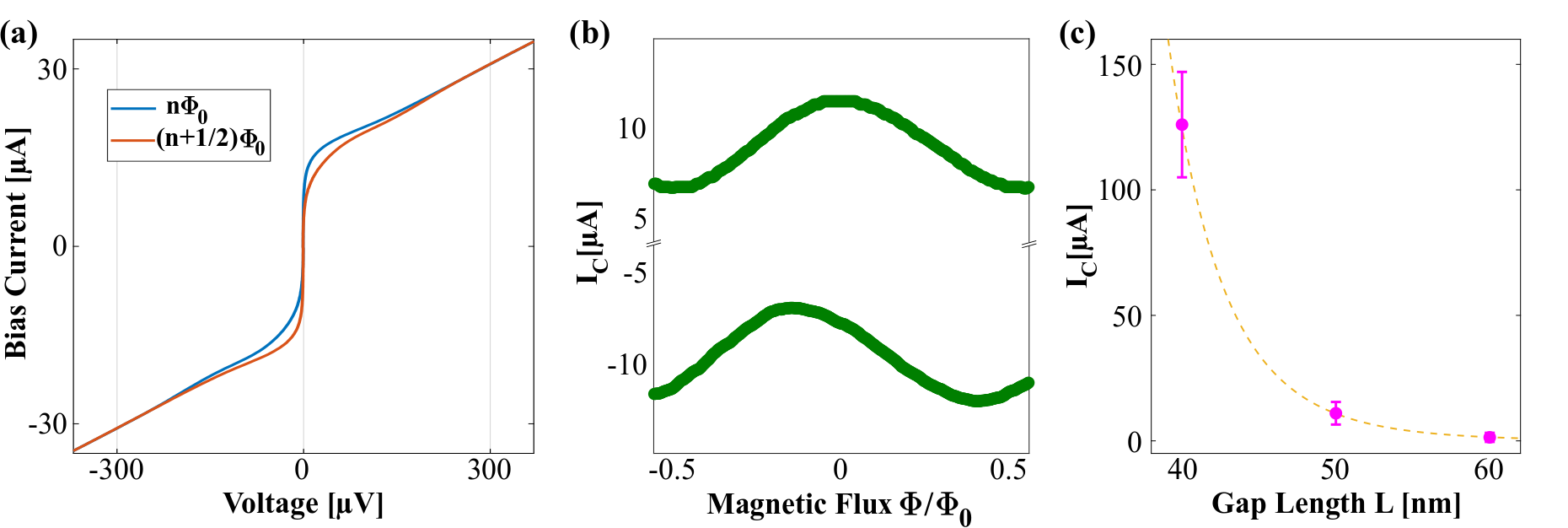
The two current voltage characteristics (IVCs) shown in Figure 3(a) for SQ1 correspond to the maximum, , and the minimum, , measured values of the positive critical current within one modulation period. Figure 3(b) shows the modulation of the critical current, , where is the applied magnetic flux. Similarly to what has been shown in our previous works on Dayem bridge SQUIDs 8, 11, 12, our GDB based SQUIDs exhibit modulations of the critical current as a function of the externally applied magnetic flux. The IVCs and modulation for SQ2 are reported in the supporting information showing similar behavior as SQ1.
The shape of the IVC resembles that of a resistively shunted junction (RSJ) similar to junctions defined with a focused helium ion beam 27, indicative of a superconductor-normal conductor-superconductor (SNS) type of junction at K. The RSJ-like behavior persists down to K (see supporting information), a feature not observed in ,e.g., oxygen irradiated bridges 32. Here it is important to point out that the characteristic voltage of GDBs V, with the differential resistance taken in the voltage range V, is at least a factor of 10 larger than He ion irradiated junctions reported in literature at K 27. The highest products at liquid nitrogen temperature have been achieved with grain boundary junctions 40, 41, with characteristic voltages in the range V. Bicrystal and step-edge JJs are generally believed to be closer to tunnel-like superconductor-insulator-superconductor (SIS) JJs and they are expected to have higher products compared to SNS-type JJs. While the characteristic voltages of GDBs presented here are lower than for grain boundary junctions, GDB-based SQUID magnetometers are in the same performance range as those realized by state-of-the-art junction technologies as will be shown below. A more in depth analysis on the properties of GDBs is beyond the scope of this letter and will be reported elsewhere.
The reproducibility of the fabrication process introduced above is supported by the small spread of the measured values at K of Grooved Dayem Bridges patterned on different chips, see Fig. 3(c). Here the gap length is varied between and nm and the bridge width is kept fixed nm. For nm, the average is A and for nm we measured an average of A. When is increased to nm, is suppressed to a few A or in most cases no supercurrent could be detected. After several cooling cycles and more than months storage at room temperature, the values of do not significant deviate from the original results.
In the following we discuss the advantages of using GDB-based SQUIDs compared to those implementing Dayem bridges: 1) the critical current density of A/cm2 is 40 times smaller than those of Dayem bridges. This allows implementing wider GDB junctions in SQUID magnetometers resulting in a smaller parasitic inductance, which scales with . Hence a larger coupling inductance (hair pin loop) can be used for increasing the effective area 4 while keeping the screening parameter near the optimal value , where is the total SQUID loop inductance; 2) the resistivity of GDBs is approximately m2, which is roughly 50 times larger than those of Dayem bridges. The larger resistivity of GDB results in an increased voltage modulation depth, reducing the contribution of the readout electronics input noise to the total flux noise, which will be discussed in the following.
The SQUID noise has been measured using a commercial Magnicon SEL-1 dc SQUID electronics 42. The system allows to perform measurements in Flux Locked Loop (FLL) mode and use current bias reversal at kHz in order to reduce the low-frequency critical current noise 43.
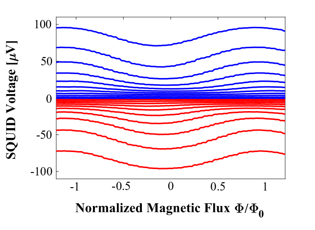
The measured voltage modulations of SQ1 as a function of magnetic flux are shown in Figure 4 for various bias current values. Each curve corresponds to an increment of the bias current equal to A. We obtain a voltage modulation depth V for values of the bias current slightly above . For the transfer function defined as max, corresponding to the maximum voltage response of the SQUID per unit of flux, we obtain V/. Indeed, a large voltage modulation depth , with the critical current modulation depth and the differential resistance of the SQUID at the working point (see supporting information) is required to achieve low noise SQUID devices. By doing so, the contribution of the amplifier input voltage noise to the white flux noise of the SQUID is minimized, hence improving the device performance.
The effective area was determined via responsivity measurements, i.e. measuring the SQUID response in FLL mode to a known magnetic field. The value of the effective area for SQ1, which is galvanically coupled to a pick-up loop with dimensions mm2, is mm2. This value is consistent with previously reported measurements performed on similar devices implementing YBCO Dayem bridges 4. The voltage noise for SQUID SQ1 was measured in FLL mode using current bias reversal. The resulting magnetic flux noise and magnetic field noise are shown in Figure 5.
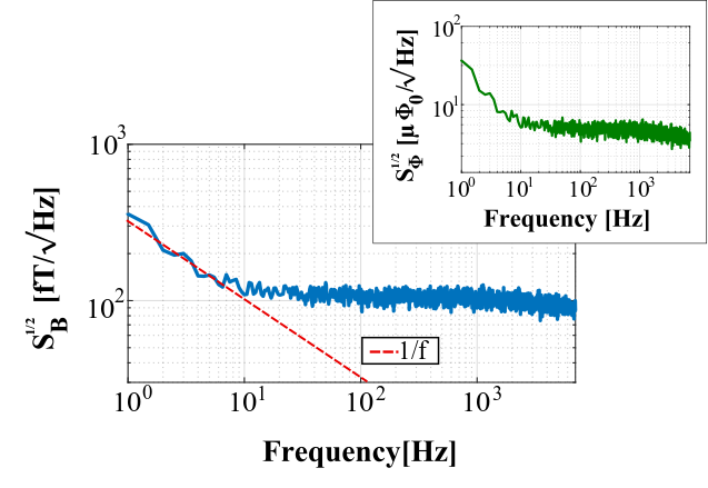
We observe a white flux noise level above the knee frequency of Hz (see inset of Figure 5). This noise value is close to the expected readout electronics input noise, . The corresponding white magnetic noise is fT (see Figure 5). This is a high level of sensitivity for a device with a much smaller pick-up loop (mm2) than standard magnetometers (mm2 and above 4, 40). Comparing these values to Dayem bridge based magnetometers 4 GDB-based devices have 10 times lower flux and magnetic field noise. This is even more remarkable considering the much smaller pick-up loop size used in this work compared to the one used in Ref. 4.
The achieved white magnetic flux noise values are comparable to state of the art single layer grain boundary junction based YBCO SQUIDs, 20, 23, 31, 22, 25. Single layer grain boundary based SQUIDs galvanically coupled to a pick-up loop of mm2 have reached white magnetic field noise values down to fT 20, 23, 31. These values are a factor lower than the one shown in Figure 5. However, considering the small size of the used pick-up loop, mm2, implemented in this work, grooved Dayem bridge based magnetometers should reach similar or even better magnetic field sensitivities for pick-up loops of lateral dimension mm. The effective area of a magnetometer, and hence the magnetic field noise, can be further improved by implementing a superconducting flux transformer in a flip-chip setup 40. Values below fT have been achieved in grain boundary JJ based devices 40. Implementing a flux transformer in our GDB based SQUID devices would indeed further improve the magnetic field sensitivity.
In conclusion, we have developed a reproducible nanopatterning procedure for the realization of YBCO Grooved Dayem Bridges. Here the layout of the bridge and the weak link across it are realized during one single lithography process on a YBCO film grown on a single crystal substrate. Such weak links have been implemented in SQUIDs galvanically coupled to a square shaped in-plane pick-up loop with lateral dimension of mm. The smaller critical current densities and larger differential resistances of the GDBs compared to bare Dayem bridges allows to implement wider bridges in SQUID application and therefore reducing the parasitic inductance. We obtained a voltage modulation depth V for a SQUID with hair pin slit length m and an effective area mm2.
The achieved magnetic field noise of fT on such a small device (mm2) paves the ground for the realization of a single layer YBCO magnetometer with magnetic field noise below fT. This could be achieved on a mm2 substrate and using a slightly longer hair pin SQUID loop. This work proves the feasibility of Grooved Dayem Bridges for the fabrication of high quality weak links and for SQUID applications. The development of low noise HTS SQUIDs is crucial not only for technological applications, such as medical diagnostic (MCG and MEG) 2, 3, 4 and geophysical surveys 1, but also in fundamental research, e.g. for magnetization measurements of nanoscale particles and single spin detection 10. Moreover, GDBs could open the way to a range of future applications, such as HTS rapid single flux quantum (RSFQ) circuits 44 and high-performance high-frequency HTS superconducting quantum interference filters (SQIFs) 45.
The authors acknowledge helpful discussions with T. Claeson and D. Montemurro. This work was been supported in part by the Knut and Alice Wallenberg Foundation (KAW) and in part by the Swedish Research Council (VR). R. A. is supported by the Swedish Research Council (VR) under the project ”Evolution of nanoscale charge order in superconducting YBCO nanostructures”.
The following files are available.
-
•
Supporting Information: Ion milling parameters summary, current voltage characteristic for SQ2, differential resistance and modulation depth as a function of bias current for both SQ1 and SQ2.
References
- Clarke 1983 Clarke, J. Geophysical applications of SQUIDs. IEEE Trans. Magn. 1983, 19, 288–294
- Koch 2001 Koch, H. SQUID magnetocardiography: Status and perspectives. IEEE Trans. Appl. Supercond. 2001, 11, 49–59
- Öisjöen et al. 2010 Öisjöen, F.; Schneiderman, J. F.; Astalan, A. P.; Kalabukhov, A.; Johansson, C.; Winkler, D. A new approach for bioassays based on frequency-and time-domain measurements of magnetic nanoparticles. Biosens. Bioelectron 2010, 25, 1008–1013
- Xie et al. 2017 Xie, M.; Chukharkin, M.; Ruffieux, S.; Schneiderman, J.; Kalabukhov, A.; Arzeo, M.; Bauch, T.; Lombardi, F.; Winkler, D. Improved coupling of nanowire-based high-T c SQUID magnetometers—simulations and experiments. Supercond. Sci. Tech. 2017, 30, 115014
- Vasyukov et al. 2013 Vasyukov, D.; Anahory, Y.; Embon, L.; Halbertal, D.; Cuppens, J.; Neeman, L.; Finkler, A.; Segev, Y.; Myasoedov, Y.; Rappaport, M. L. a. A scanning superconducting quantum interference device with single electron spin sensitivity. Nat. Nanotechnol. 2013, 8, 639
- Clarke and Braginski 2006 Clarke, J.; Braginski, A. I. The SQUID handbook: Applications of SQUIDs and SQUID systems; John Wiley & Sons, 2006
- Granata et al. 2013 Granata, C.; Vettoliere, A.; Russo, R.; Fretto, M.; De Leo, N.; Lacquaniti, V. Three-dimensional spin nanosensor based on reliable tunnel Josephson nano-junctions for nanomagnetism investigations. Appl. Phys. Lett. 2013, 103, 102602
- Arpaia et al. 2014 Arpaia, R.; Arzeo, M.; Nawaz, S.; Charpentier, S.; Lombardi, F.; Bauch, T. Ultra low noise YBa2Cu3O7- nano superconducting quantum interference devices implementing nanowires. Appl. Phys. Lett. 2014, 104, 072603
- Wölbing et al. 2014 Wölbing, R.; Schwarz, T.; Müller, B.; Nagel, J.; Kemmler, M.; Kleiner, R.; Koelle, D. Optimizing the spin sensitivity of grain boundary junction nanoSQUIDs—towards detection of small spin systems with single-spin resolution. Supercond. Sci. Technol. 2014, 27, 125007
- Schwarz et al. 2015 Schwarz, T.; Wölbing, R.; Reiche, C. F.; Müller, B.; Martínez-Pérez, M.-J.; Mühl, T.; Büchner, B.; Kleiner, R.; Koelle, D. Low-noise YBa 2 Cu 3 O 7 nano-SQUIDs for performing magnetization-reversal measurements on magnetic nanoparticles. Phys. Rev. Appl. 2015, 3, 044011
- Arzeo et al. 2016 Arzeo, M.; Arpaia, R.; Baghdadi, R.; Lombardi, F.; Bauch, T. Toward ultra high magnetic field sensitivity YB a 2 C u 3 O 7- nanowire based superconducting quantum interference devices. J. Appl. Phys. 2016, 119, 174501
- Arpaia et al. 2016 Arpaia, R.; Arzeo, M.; Baghdadi, R.; Trabaldo, E.; Lombardi, F.; Bauch, T. Improved noise performance of ultrathin YBCO Dayem bridge nanoSQUIDs. Supercond. Sci. Technol. 2016, 30, 014008
- Chen et al. 2016 Chen, L.; Wang, H.; Liu, X.; Wu, L.; Wang, Z. A High-performance Nb nano-superconducting quantum interference device with a three-dimensional structure. Nano Lett. 2016, 16, 7726–7730
- Russo et al. 2016 Russo, R.; Esposito, E.; Crescitelli, A.; Di Gennaro, E.; Granata, C.; Vettoliere, A.; Cristiano, R.; Lisitskiy, M. NanoSQUIDs based on niobium nitride films. Supercond. Sci. Technol. 2016, 30, 024009
- Martínez-Pérez and Koelle 2016 Martínez-Pérez, M. J.; Koelle, D. NanoSQUIDs: Basics & recent advances. Phys. Sci. Rev. 2016, 2
- Granata and Vettoliere 2016 Granata, C.; Vettoliere, A. Nano superconducting quantum interference device: A powerful tool for nanoscale investigations. Phys. Rep. 2016, 614, 1–69
- Schneiderman 2014 Schneiderman, J. F. Information content with low-vs. high-Tc SQUID arrays in MEG recordings: The case for high-Tc SQUID-based MEG. J. Neurosci. Methods 2014, 222, 42–46
- Xie et al. 2017 Xie, M.; Schneiderman, J. F.; Chukharkin, M. L.; Kalabukhov, A.; Riaz, B.; Lundqvist, D.; Whitmarsh, S.; Hämäläinen, M.; Jousmäki, V.; Oostenveld, R.; Winkler, D. Benchmarking for on-scalp MEG sensors. IEEE Trans. Biomed. Eng. 2017, 64, 1270–1276
- Riaz et al. 2017 Riaz, B.; Pfeiffer, C.; Schneiderman, J. F. Evaluation of realistic layouts for next generation on-scalp MEG: spatial information density maps. Sci. Rep. 2017, 7, 6974
- Öisjöen et al. 2012 Öisjöen, F.; Schneiderman, J. F.; Figueras, G.; Chukharkin, M.; Kalabukhov, A.; Hedström, A.; Elam, M.; Winkler, D. High-T c superconducting quantum interference device recordings of spontaneous brain activity: Towards high-T c magnetoencephalography. Appl. Phys. Lett. 2012, 100, 132601
- Lee et al. 1995 Lee, L.; Teepe, M.; Vinetskiy, V.; Cantor, R.; Colclough, M. Key elements for a sensitive 77 K direct current superconducting quantum interference device magnetometer. Applied physics letters 1995, 66, 3058–3060
- Faley et al. 2013 Faley, M.; Poppe, U.; Dunin-Borkowski, R.; Schiek, M.; Boers, F.; Chocholacs, H.; Dammers, J.; Eich, E.; Shah, N.; Ermakov, A. High-Tc DC SQUIDS for magnetoencephalography. IEEE Trans. Appl. Supercond. 2013, 23, 1600705–1600705
- Chukharkin et al. 2013 Chukharkin, M.; Kalabukhov, A.; Schneiderman, J. F.; Öisjöen, F.; Jönsson, M.; Xie, M.; Snigirev, O. V.; Winkler, D. Improvement of ultra-low field magnetic resonance recordings with a multilayer flux-transformer-based high-Tc SQUID magnetometer. IEEE Trans. Appl. Supercond. 2013, 23
- Chesca et al. 2015 Chesca, B.; John, D.; Mellor, C. J. Flux-coherent series SQUID array magnetometers operating above 77 K with superior white flux noise than single-SQUIDs at 4.2 K. Applied Physics Letters 2015, 107, 162602
- Mitchell and Foley 2010 Mitchell, E.; Foley, C. YBCO step-edge junctions with high IcRn. Supercond. Sci. Technol. 2010, 23, 065007
- Tinchev 2007 Tinchev, S. S. Mechanism of operation of josephson junctions made from htc materials by ion modification. Physica C: Superconductivity 2007, 460, 1477–1478
- Cybart et al. 2015 Cybart, S. A.; Cho, E.; Wong, T.; Wehlin, B. H.; Ma, M. K.; Huynh, C.; Dynes, R. Nano Josephson superconducting tunnel junctions in YBa 2 Cu 3 O 7– directly patterned with a focused helium ion beam. Nat. Nanotech. 2015, 10, 598
- Cho et al. 2015 Cho, E.; Ma, M.; Huynh, C.; Pratt, K.; Paulson, D.; Glyantsev, V.; Dynes, R.; Cybart, S. A. YBa2Cu3O7- superconducting quantum interference devices with metallic to insulating barriers written with a focused helium ion beam. Appl. Phys. Lett. 2015, 106, 252601
- Cho et al. 2018 Cho, E. Y.; Li, H.; LeFebvre, J. C.; Zhou, Y. W.; Dynes, R.; Cybart, S. A. Direct-coupled micro-magnetometer with Y-Ba-Cu-O nano-slit SQUID fabricated with a focused helium ion beam. Applied physics letters 2018, 113, 162602
- Tinchev 1993 Tinchev, S. High-T/sub c/SQUIDS with local oxygen-ion irradiated weak links. IEEE transactions on applied superconductivity 1993, 3, 28–32
- Faley et al. 2014 Faley, M.; Meertens, D.; Poppe, U.; Dunin-Borkowski, R. Graphoepitaxial high-Tc SQUIDs. Journal of Physics: Conference Series. 2014; p 042009
- Bergeal et al. 2006 Bergeal, N.; Lesueur, J.; Faini, G.; Aprili, M.; Contour, J. High T c superconducting quantum interference devices made by ion irradiation. Applied physics letters 2006, 89, 112515
- Foley 1999 Foley, C. Fabrication and characterisation of YBCO single grain boundary step edge junctions. IEEE Trans. Appl. Supercond. 1999, 9, 4281–4284
- Nawaz et al. 2013 Nawaz, S.; Arpaia, R.; Lombardi, F.; Bauch, T. Microwave Response of Superconducting Y Ba 2 Cu 3 O 7- Nanowire Bridges Sustaining the Critical Depairing Current: Evidence of Josephson-like Behavior. Phys. Rev. Lett. 2013, 110, 167004
- Nawaz et al. 2013 Nawaz, S.; Arpaia, R.; Bauch, T.; Lombardi, F. Approaching the theoretical depairing current in YBa2Cu3O7- x nanowires. Physica C Supercond 2013, 495, 33–38
- Trabaldo et al. 2017 Trabaldo, E.; Arzeo, M.; Arpaia, R.; Baghdadi, R.; Andersson, E.; Lombardi, F.; Bauch, T. Noise properties of YBCO Nanostructures. IEEE Trans. Appl. Supercond. 2017, 27
- Arpaia et al. 2018 Arpaia, R.; Andersson, E.; Trabaldo, E.; Bauch, T.; Lombardi, F. Probing the phase diagram of cuprates with YBa 2 Cu 3 O 7- thin films and nanowires. Phys. Rev. Mater. 2018, 2, 024804
- Manos and Flamm 1989 Manos, D. M.; Flamm, D. L. Plasma etching: an introduction; Elsevier, 1989
- Johansson et al. 2009 Johansson, J.; Cedergren, K.; Bauch, T.; Lombardi, F. Properties of inductance and magnetic penetration depth in (103)-oriented YBa 2 Cu 3 O 7- thin films. Phys. Rev. B 2009, 79, 214513
- Faley et al. 2017 Faley, M.; Dammers, J.; Maslennikov, Y.; Schneiderman, J.; Winkler, D.; Koshelets, V.; Shah, N.; Dunin-Borkowski, R. High-Tc SQUID biomagnetometers. Superconductor Science and Technology 2017, 30, 083001
- Poppe et al. 2001 Poppe, U.; Divin, Y.; Faley, M.; Wu, J.; Jia, C.; Shadrin, P.; Urban, K. Properties of YBa/sub 2/Cu/sub 3/O/sub 7/thin films deposited on substrates and bicrystals with vicinal offcut and realization of high I/sub c/R/sub n/junctions. IEEE transactions on applied superconductivity 2001, 11, 3768–3771
- 42 Magnicon, SQUID electronics SEL-1, http://www.magnicon.com
- Drung 2003 Drung, D. High-Tc and low-Tc dc SQUID electronics. Supercond. Sci. Technol. 2003, 16, 1320
- Wolf et al. 2013 Wolf, T.; Bergeal, N.; Lesueur, J.; Fourie, C. J.; Faini, G.; Ulysse, C.; Febvre, P. YBCO Josephson junctions and striplines for RSFQ circuits made by ion irradiation. IEEE Transactions on applied superconductivity 2013, 23, 1101205–1101205
- Mitchell et al. 2016 Mitchell, E.; Hannam, K.; Lazar, J.; Leslie, K.; Lewis, C.; Grancea, A.; Keenan, S.; Lam, S.; Foley, C. 2D SQIF arrays using 20 000 YBCO high R n Josephson junctions. Supercond. Sci. Technol. 2016, 29, 06LT01