Dark-field second harmonic generation imaging of grain boundaries in 2D semiconducting transition metal dichalcogenides
Bruno R. Carvalho1,∗, Yuanxi Wang2,3,4, Kazunori Fujisawa2,3, Tianyi Zhang3,5, Ethan Kahn3,5, Ismail Bilgin6, Pulickel M. Ajayan7, Ana M. de Paula8, Marcos A. Pimenta8, Swastik Kar6, Vincent H. Crespi2,3,4, Mauricio Terrones2,3,5 & Leandro M. Malard8,∗
1 Departamento de Física, Universidade Federal do Rio Grande do Norte, Natal, Rio Grande do Norte 59078-970, Brazil
2 Department of Physics, The Pennsylvania State University, University Park, PA 16802, USA
3 Center for 2-Dimensional and Layered Materials, The Pennsylvania State University, University Park, PA 16802, USA
4 2-Dimensional Crystal Consortium, The Pennsylvania State University, University Park, PA 16802, USA
5 Department of Materials Science and Engineering, The Pennsylvania State University, University Park, PA 16802, USA
6 Department of Physics, Northeastern University, Boston, Massachusetts 02115, USA
7 Department of Material Science and NanoEngineering, Rice University, Houston, TX, 77005, United States
8 Departamento de Física, Universidade Federal de Minas Gerais, Belo Horizonte, Minas Gerais 30123-970, Brazil
∗E-mail: brunorc@fisica.ufrn.br (B.R.C.) and lmalard@fisica.ufmg.br (L.M.M.).
A material’s quality often determines its identity at both a fundamental and applied level. For example, the fractional quantum Hall effect simply does not exist in heterostructures of insufficient crystalline quality [1, 2, 3], while silicon wafers [4, 5, 6] or non-linear crystals [7, 8] of low crystalline purity are electronically or optically useless. Even when surface states are topologically protected their visibility depends critically on obtaining extremely high crystalline quality in the bulk regions [9]. Extended defects with one dimensionality smaller than that of the host, such as 2D grain boundaries in 3D materials or 1D grain boundaries in 2D materials, can be particularly damaging since they directly impede the transport of charge, spin or heat, and can introduce a metallic character into otherwise semiconducting systems. Unfortunately, a technique to rapidly and non-destructively image 1D defects in 2D materials is lacking. Scanning transmission electron microscopy (STEM) [10, 11, 12, 13], Raman [14, 15], photoluminescence [16, 17, 10, 12] and nonlinear optical spectroscopies [18, 19], are all extremely valuable, but current implementations suffer from low throughput and a destructive nature (STEM) or limitations in their unambiguous sensitivity at the nanoscale. Here we demonstrate that dark-field second harmonic generation (SHG) microscopy can rapidly, efficiently, and non-destructively probe grain boundaries and edges in monolayer dichalcogenides (i.e. MoSe2, MoS2 and WS2). Dark-field SHG efficiently separates the spatial components of the emitted light and exploits interference effects from crystal domains of different orientations to localize grain boundaries and edges as very bright 1D patterns through a Čerenkov-type SHG emission. The frequency dependence of this emission in MoSe2 monolayers is explained in terms of plasmon-enhanced SHG related to the defect’s metallic character. This new technique for nanometer-scale imaging of the grain structure, domain orientation and localized 1D plasmons in 2D different semiconductors, thus enables more rapid progress towards both applications and fundamental materials discoveries.
Atomically thin 2D semiconductor transition metal dichalcogenides (TMDs) host a diversity of excitons with robust light-valley coupling and exciton-defect coupling that allows spectroscopic characterization [20, 21, 22]. Different techniques have been employed to characterize 1D defects in these 2D systems to evaluate sample crystalline quality for potential device applications [22]. Transmission electron microscopy directly resolves atomistic details of defects [23, 24, 10, 11, 12, 13], but requires intensive and disruptive sample preparation. Photoluminescence and Raman spectroscopy provide rapid and non-destructive probes of the electronic and vibrational properties of defective regions [10, 12, 16, 19], which often manifest as red- or blue-shifted emission with enhanced or suppressed intensities when compared to the response from a pristine crystal, depending on multiple factors that affect local electronic properties such as material composition, doping level, defect passivation [25], grain boundary (GB) geometry [10] or edge terminations [26]. This complicates their use as means of reproducible defect characterization. Therefore, a more reliable and facile method to effectively image grain boundaries and edges independent of composition, doping, and defect reconstruction, is needed. Recent reports show that nonlinear optical spectroscopy is highly sensitive for imaging 1D imperfections [18, 19]; nonetheless, their visualization exhibited a weak background contrast [18] or required the use of chemical solvents to enhance image contrast [19].
Dark-field (DF) microscopy boost image contrast by suppressing light scattered from the homogeneous regions. The technique does not depend on the detailed local atomic and electronic structure, i.e. sharp discontinuities always appear brighter. When comparing a bright-field (BF) linear optical image of a monolayer MoS2 on quartz (Supplementary Figure S1a), and a DF linear optical image (i.e. incident and collected light of the same frequency, Supplementary Figure S1b), we observe in DF light scattered from the edges that are transparent to BF microscopy. However, atomically thin grain boundaries cannot be resolved by either imaging technique, because the in-plane linear dielectric response of MoS2 monolayers is isotropic so radiation dipoles generated by two grains separated by a GB are always in phase, making the scattered light intensity near a GB indistinguishable from that in the pristine region, even in dark field imaging. (The bright dots in the DF image are due to contaminants from the transfer process, see Methods section). In stark contrast, second harmonic radiation dipoles (emitting frequency-doubled photons) in two grains separated by a mirror boundary are always out of phase, thus creating interference that can be detected as a localized feature. Here we develop a dark-field nonlinear characterization technique combining SHG microscopy and a spatial filter, to further enhance the second harmonic contrast of 1D imperfections in 2D systems, thus allowing detailed large-area spatial mapping of grain boundaries and edges regardless of their local atomic and electronic structures.
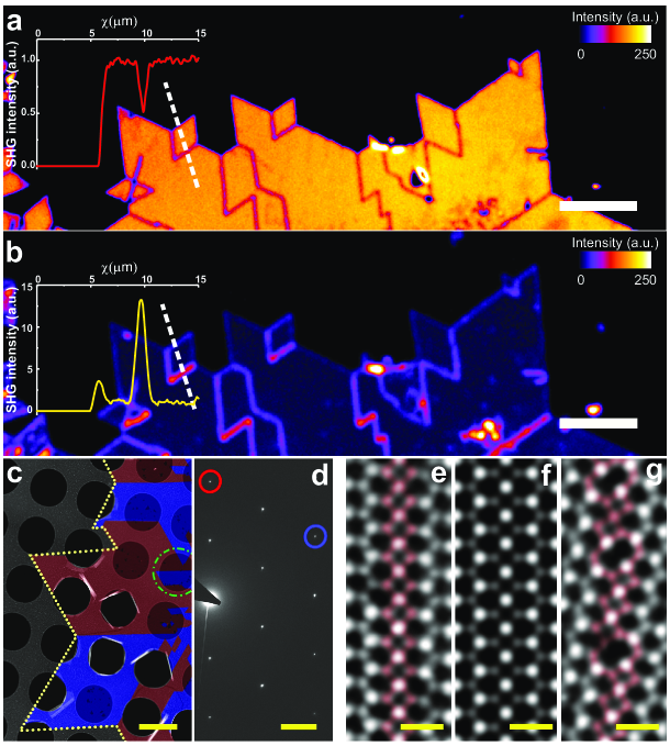
Monolayer TMDs grown by chemical vapour deposition (see Methods) were characterized using a picosecond laser system tunable from 1.30 to 1.65 eV. SHG microscopy was performed using a high numerical aperture objective in a back-reflected geometry (details in Methods). We employed a DF filter (patch stop) in front of the detector to collect only light with large wave-vectors (see Supplementary Note S2). Figures 1a,b show BF- and DF-SHG images of monolayer MoSe2 for a pump beam of 1.38 eV (900 nm), where the uniform SHG intensities in interior of each grain confirms their single-layer nature [18, 19]. A dark GB in Fig. 1a is ascribed to destructive interference of the SHG signals generated from neighboring grains with opposite orientations [18, 19]. The DF-SHG response (Fig. 1b) of the central region is considerably suppressed as a result of the DF filter blocking SHG emission from the bulk, leaving GBs and edges now as bright emission features.
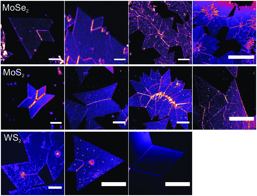
To estimate the contrast difference between BF- and DF-SHG, line-scans (dashed white line) are performed along the grain boundaries, edges and bulk regions (insets Figs. 1a,b); normalized by the bulk signal. We define a 1D-defect contrast factor as , where and are the SHG responses of the GB/edge and the bulk; this contrast can be calculated for both dark () and bright () fields. The line profiles of Figs. 1a,b yield a three-fold contrast enhancement from the grain boundary under dark-field conditions, , and a dramatic 20-fold enhancement from the edge, . To establish the potential of this technique, Figure 2 shows DF-SHG imaging for several additional monolayers of MoSe2, MoS2 and WS2. All show strong contrast enhancements, with some variations arising from variations in sample size and optimization of the patch stop position. These results show the great potential of DF-SHG as a novel highly sensitive, non-invasive probe to effectively reveal structural discontinuities in 2D semiconductors without the use of chemical solvents, with fast image rates and high spatial resolutions compared to other optical spectroscopy techniques when imaging the same type of defects [10, 12, 18, 16, 19] (Supplementary Movies S1 and S2 show a fast and large area DF-SHG scan).
To explain the DF-SHG process near a MoSe2 GB, we first determine its atomic structure using aberration-corrected high-resolution scanning transmission electron microscopy (AC-HRSTEM). Figure 1c shows a low-magnification STEM image of monolayer MoSe2. A high-angle annular dark field (HAADF) detector was used for STEM imaging and the edge of the MoSe2 flake is highlighted by a yellow dotted line. Electron diffraction (Fig. 1d) acquired from the area circled in green in Fig. 1c shows a pair of first-order hexagonal diffraction spots. Placing an objective aperture at selected diffraction spots yields DF-TEM images (Supplementary Figure S3) that are overlaid with the original STEM-HAADF image (Fig. 1c) to reveal two mirror twin grains with opposite orientations, colored in red or blue in Fig. 1d. Detailed atomic images of GBs include the 44 motifs aligned along the zigzag direction (Figure 1e,f), and 48 reconstructions that introduce tilts and kinks (Figure 1g and Supplementary Figure S4) [23, 24].
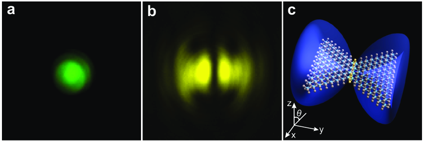
With the atomic grain structure determined, we now discuss the mechanism behind the increased contrast of 1D defects in the DF-SHG images. Figures 3a,b shows a second harmonic far-field spatial mode that results when the pump beam (at 950 nm) is focused on the center of the MoSe2 monolayer (2D bulk) and GB, respectively. The far-field second harmonic pattern of the 2D bulk (green circle) preserves the circular symmetry of the Gaussian distribution of the incident light. In contrast, the second harmonic emission from the GB has a dark central stripe with additional arc features at large angles as shown in Fig. 3b. Since mirror grains have opposite polarities () and switch the sign of the second-order nonlinear susceptibility , the out-of-phase second harmonic electric field radiated from mirror grains will interfere destructively along small angles (with respect to the normal of the sample plane, inset in Figure 3), as can be described within a dipole model (see Supplementary Note S4). This explains the dark stripe in Fig. 3b [18]. On the other hand, larger can compensate for the phase offset from the two mirror grains, as constructive interference following , where is the distance between the two grains within a laser spot size (radius of the Gaussian profile), and the SHG wavelength ( nm). Figure 3c depicts this situation, where two anti-parallel domains give rise to a second harmonic emission that is directed at larger angles , as shown by the calculated 3D surface radiation (Fig. 3c). Therefore, the SHG response from GB regions is emitted at larger angles, yielding the arc features shown in Fig. 3b and calculated in Fig. 3c. The effective spot size corresponds to nm, as obtained from the SHG image analysis considering a Gaussian profile. We can thus estimate the direction of constructive interference to be at , close to the 32∘ measured from the far-field pattern (Fig. 3b and Supplementary Note S5 for angle determination).
A similar anisotropy in second harmonic radiation has been observed for inversion domain boundaries in bulk nonlinear crystals, where due to the large thickness of the crystals phase matching can also occur, leading to so-called Čerenkov phase-matched second harmonic emission [27, 28]. In fact, any sharp discontinuity in leads to this type of anisotropic second harmonic radiation. In the present case, the symmetry of the GB requires that and the sample’s edges require due to the termination of nonlinear material [29, 30, 31, 32]. In our DF-SHG experiment, the patch stop removes the SHG radiation emitted at small angles, thereby favoring emission from 1D GBs and edges in semiconducting TMDs (Figs. 1, 2).
We next explore the GB DF-SHG signal for different fundamental photon energies. Figure 4a shows the DF-SHG amplitude dependence on the photon energy for bulk (red squares) and GB (green spheres) from monolayer MoSe2 from 1.32 to 1.65 eV (Supplementary Note S6 shows similar data from an edge). The DF-SHG bulk emission shows an onset of optical transitions at 1.55 eV, which has been attributed to a resonance close to the exciton energy [33], where the energy of one of the two photons equals the optical gap (so-called resonance). For excitations between 1.32 and 1.51 eV, the weak resonance near 1.3 eV for the bulk emission can be associated to a two-photon resonance ( resonance), where twice the photon energy matches the C exciton energy or other low-energy states due to structural defects present within the bulk crystal lattice [34]. By contrast, the DF-SHG GB emission shows a strong resonance at 1.32 eV compared to the bulk case, yielding an enhanced contrast between the two signals.
Constructive interference alone would yield a near-constant intensity ratio between the GB and the bulk emission as a function of frequency, which is not the case here. Thus, the strong frequency dependence shown in Fig. 4a indicates the presence of additional SHG-modulating processes. Similar frequency-dependent BF-SHG intensities from 1D defects in MoS2 have been reported [26, 18] where the measured edge SHG enhancement reaches 1.4 at half the optical gap of MoS2. If a nm wide edge region (effective edge thickness taken in Ref. 18) within a 1 m laser spot amplifies the SHG by 1.4 times, the amplification factor intrinsic to the edge would be about 400 (Supplementary Note S7 gives more details).
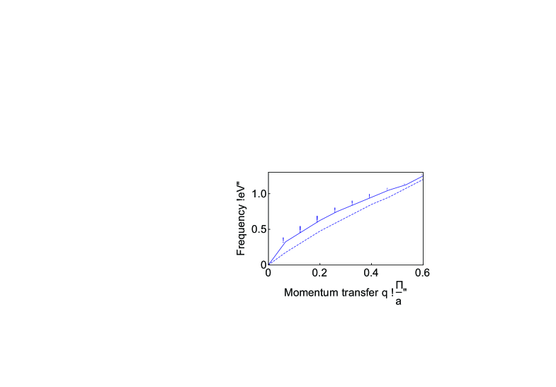
The selectivity of the SHG contrast enhancement to the spectral range below the MoSe2 optical gap of 1.5 eV, and the order-of-magnitude amplification inferred above from previous work [26, 18], are characteristic of plasmon resonances: strongly localized electric fields confined within 1D nanowires can amplify the optical response of the host material [35]. Momentum conservation in such plasmon-mediated SHG processes can be achieved by the annihilation of two counter-propagating plasmons in 2D [36, 37] or coupled 1D+2D systems [38]. Plasmons in MoSe2 samples originate from metallic states localized at mirror grain boundaries (Supplementary Note S7). To show that plasmon enhancement in SHG are limited to 1.5 eV, we calculate the energy range in which the plasmon localized on the GB carries a significant spectral weight, as can be characterized by the calculated mode-specific electron energy loss spectra (EELS). Although photons cannot provide the large wave-vectors needed to excite plasmons localized along a pristine GB and although the longitudinal dielectric response is calculated here (accessible to EELS but not to optical spectroscopy), the breaking of translational symmetry by kinks along the GB (Fig. 1g) could supply the required momentum and allow photon-plasmon coupling, similar to that seen in bent nanowires [39] and finite-length 1D metallic quantum wires [40, 41]. This assumption is consistent with kink patterns observed in STEM (Fig. 1g and Supplementary Figure S4). Thus, we only consider the calculated EELS to reveal available plasmonic states in an ideal 1D GB, and assume the presence of sufficient translational symmetry breaking to activate plasmon-photon coupling.
The calculated mode-specific EELS, , is shown in Figure 4b, where we select the mode index for the plasmon localized on the 44 GB (Supplementary Note S7). As the momentum transfer increases from 0 to 0.6 , where is the MoSe2 lattice constant 3.29 Å, the spectral weight of the plasmon localized on the 44 GB decreases towards zero as the plasmon peak energy approaches 1.5 eV. This plasmon dispersion is shown in Figure 4c (solid curve), where the circle sizes are proportional to plasmon spectral weights. The dispersion for intra-band transition resonances, , are plotted in a dashed line. Since each plasmon peak is determined by , the decrease in the EELS peak spectral weight, , means that the imaginary part of the dielectric function is increasing due to the increasing contributions from inter-band transitions as the excitation energy approaches the band gap, i.e. plasmons become damped by inter-band transitions approaching the 1.5 eV gap [42]. The calculated existence of a 1D plasmon mode and its complete damping beyond 1.5 eV are consistent with the measured SHG amplification only below 1.5 eV, as shown in Fig. 4a.
In conclusion, dark-field SHG microscopy provides rapid, high-contrast, non-destructive mapping of 1D defects in atomically thin 2D TMDs due to an interference-enhanced directional confinement of the nonlinear response across the 1D defect in a manner analogous to the Čerenkov phase-matched second harmonic emission. The observed frequency-dependent DF-SHG enhancement near the grain boundary suggests a prominent plasmon-modulated nonlinear optical response at 1D defects in atomically thin TMDs. Our results provide a direct pathway to electronically map the SHG response of 1D defects acting as nanoantennae within a 2D layered TMD, potentially applicable to other classes of 2D systems.
Methods
Methods, including statements of data availability and any associated accession codes and references, are available at Supplementary Information.
Data availability.
All relevant data are available from the authors upon request.
Acknowledgments
B.R.C., A.M.dP., M.A.P., and L.M.M. acknowledge the financial support from the Brazilian agencies CNPq, CAPES, FAPEMIG and Brazilian Institute of Science and Technology of Nanocarbon (INCT-Nanocarbono) and Molecular Medicine (INCT-Medicina Molecular). Y.W. and V.H.C acknowledge support from the National Science Foundation 2-Dimensional Crystal Consortium - Materials Innovation Platform (2DCC-MIP) under DMR-1539916. K.F., P.M.A. and M.T. acknowledge The Air Force Office of Scientific Research (AFOSR) grant 17RT0244 for financial support. T.Z. and M. T. also thank the financial support from the National Science Foundation (2DARE-EFRI-1433311). S.K. acknowledges financial support from NSF ECCS 1351424.
Author contributions
B.R.C. and L.M.M. conceived the idea and designed the experiments. B.R.C. and L.M.M. performed the nonlinear optical experiments. A.M.dP. contributed to the nonlinear experiment in its early phase. B.R.C. and M.A.P. performed the Raman experiments. B.R.C. analyzed and interpreted the nonlinear and Raman experimental data. Y.W. and V.H.C. performed the theoretical work. K.F., T.Z., E.K. and M.T. performed the scanning transmission electron measurements and synthesized the MoS2 and WS2 monolayers. I.B., S.K. and P.M.A. synthesized the MoSe2 flakes. B.R.C., Y.W. and L.M.M. wrote the manuscript. All the authors discussed the results and commented on the manuscript.
Competing interests
The authors declare no competing financial interests.
Additional information
Supplementary Information
accompanies this paper at
Correspondence and requests for materials
should be addressed to B.R.C. or L.M.M.
References
- [1] X. Du, I. Skachko, F. Duerr, A. Luican, and E. Y. Andrei, “Fractional quantum hall effect and insulating phase of dirac electrons in graphene,” Nature, vol. 462, no. 7270, p. 192, 2009.
- [2] K. I. Bolotin, F. Ghahari, M. D. Shulman, H. L. Stormer, and P. Kim, “Observation of the fractional quantum hall effect in graphene,” Nature, vol. 462, no. 7270, p. 196, 2009.
- [3] C. R. Dean et al., “Multicomponent fractional quantum hall effect in graphene,” Nat. Phys., vol. 7, no. 9, p. 693, 2011.
- [4] A. H. Atabaki et al., “Integrating photonics with silicon nanoelectronics for the next generation of systems on a chip,” Nature, vol. 556, no. 7701, p. 349, 2018.
- [5] S. W. Boettcher et al., “Energy-conversion properties of vapor-liquid-solid–grown silicon wire-array photocathodes,” Science, vol. 327, no. 5962, pp. 185–187, 2010.
- [6] E. Garnett and P. Yang, “Light trapping in silicon nanowire solar cells,” Nano Lett., vol. 10, no. 3, pp. 1082–1087, 2010.
- [7] D. N. Nikogosyan, Nonlinear optical crystals: a complete survey. Springer Science & Business Media, 2005.
- [8] P. A. Morris, “Impurities in nonlinear optical oxide crystals,” J. Cryst. Growth, vol. 106, no. 1, pp. 76–88, 1990.
- [9] E. Wang et al., “Fully gapped topological surface states in bi2se3 films induced by a d-wave high-temperature superconductor,” Nat. Phys., vol. 9, no. 10, p. 621, 2013.
- [10] A. M. Van Der Zande et al., “Grains and grain boundaries in highly crystalline monolayer molybdenum disulphide,” Nat. Mater., vol. 12, no. 6, p. 554, 2013.
- [11] S. Najmaei et al., “Vapour phase growth and grain boundary structure of molybdenum disulphide atomic layers,” Nat. Mater., vol. 12, no. 8, p. 754, 2013.
- [12] Z. Liu et al., “Strain and structure heterogeneity in MoS2 atomic layers grown by chemical vapour deposition,” Nat. Commun., vol. 5, p. 5246, 2014.
- [13] A. Azizi et al., “Dislocation motion and grain boundary migration in two-dimensional tungsten disulphide,” Nat. Commun., vol. 5, p. 4867, 2014.
- [14] L. G. Cançado et al., “Quantifying defects in graphene via raman spectroscopy at different excitation energies,” Nano Lett., vol. 11, no. 8, pp. 3190–3196, 2011.
- [15] S. Mignuzzi et al., “Effect of disorder on Raman scattering of single-layer ,” Phys. Rev. B, vol. 91, no. 19, p. 195411, 2015.
- [16] V. Carozo et al., “Optical identification of sulfur vacancies: Bound excitons at the edges of monolayer tungsten disulfide,” Sci. Adv., vol. 3, no. 4, p. e1602813, 2017.
- [17] T. V. Alencar, L. M. Malard, and A. M. de Paula, “Supercollision cooling effects on the hot photoluminescence emission of graphene,” Nanotechnology, vol. 27, no. 44, p. 445710, 2016.
- [18] X. Yin et al., “Edge Nonlinear Optics on a MoS2 Atomic Monolayer,” Science, vol. 344, no. 6183, pp. 488–490, 2014.
- [19] L. Karvonen et al., “Rapid visualization of grain boundaries in monolayer MoS2 by multiphoton microscopy,” Nat. Commun., vol. 8, p. 15714, 2017.
- [20] X. Xu, W. Yao, D. Xiao, and T. F. Heinz, “Spin and pseudospins in layered transition metal dichalcogenides,” Nat. Phys., vol. 10, pp. 343–350, 2014.
- [21] K. F. Mak and J. Shan, “Photonics and optoelectronics of 2D semiconductor transition metal dichalcogenides,” Nat. Photonics, vol. 10, no. 4, p. 216, 2016.
- [22] Z. Lin et al., “Defect engineering of two-dimensional transition metal dichalcogenides,” 2D Materials, vol. 3, no. 2, p. 022002, 2016.
- [23] W. Zhou et al., “Intrinsic structural defects in monolayer molybdenum disulfide,” Nano Lett., vol. 13, no. 6, pp. 2615–2622, 2013.
- [24] O. Lehtinen et al., “Atomic Scale Microstructure and Properties of Se-Deficient Two-Dimensional MoSe2,” ACS Nano, vol. 9, no. 3, pp. 3274–3283, 2015.
- [25] H. Nan et al., “Strong Photoluminescence Enhancement of MoS2 through Defect Engineering and Oxygen Bonding,” ACS Nano, vol. 8, pp. 5738–5745, jun 2014.
- [26] K.-I. Lin et al., “Atom-Dependent Edge-Enhanced Second-Harmonic Generation on MoS2 Monolayers,” Nano Lett., vol. 18, no. 2, pp. 793–797, 2018.
- [27] A. R. Tunyagi, M. Ulex, and K. Betzler, “Noncollinear optical frequency doubling in strontium barium niobate,” Phys. Rev. Lett., vol. 90, p. 243901, 2003.
- [28] Y. Sheng, A. Best, H.-J. Butt, W. Krolikowski, A. Arie, and K. Koynov, “Three-dimensional ferroelectric domain visualization by Čerenkov-type second harmonic generation,” Opt. Express, vol. 18, no. 16, pp. 16539–16545, 2010.
- [29] Y. Sheng, V. Roppo, K. Kalinowski, and W. Krolikowski, “Role of a localized modulation of in Čerenkov second-harmonic generation in nonlinear bulk medium,” Opt. Lett., vol. 37, no. 18, pp. 3864–3866, 2012.
- [30] H. Ren, X. Deng, Y. Zheng, N. An, and X. Chen, “Enhanced nonlinear Čherenkov radiation on the crystal boundary,” Opt. Lett., vol. 38, no. 11, pp. 1993–1995, 2013.
- [31] V. Roppo, K. Kalinowski, Y. Sheng, W. Krolikowski, C. Cojocaru, and J. Trull, “Unified approach to Čerenkov second harmonic generation,” Opt. Express, vol. 21, no. 22, pp. 25715–25726, 2013.
- [32] X. Zhao, Y. Zheng, H. Ren, N. An, X. Deng, and X. Chen, “Nonlinear Čherenkov radiation at the interface of two different nonlinear media,” Opt. Express, vol. 24, no. 12, pp. 12825–12830, 2016.
- [33] D. H. Kim and D. Lim, “Optical second-harmonic generation in few-layer MoSe2,” J. Korean Phys. Soc., vol. 66, no. 5, pp. 816–820, 2015.
- [34] S. Refaely-Abramson, D. Y. Qiu, S. G. Louie, and J. B. Neaton, “Defect-induced modification of low-lying excitons and valley selectivity in monolayer transition metal dichalcogenides,” Phys. Rev. Lett., vol. 121, p. 167402, 2018.
- [35] K. M. Goodfellow, R. Beams, C. Chakraborty, L. Novotny, and A. N. Vamivakas, “Integrated nanophotonics based on nanowire plasmons and atomically thin material,” Optica, vol. 1, no. 3, p. 149, 2014.
- [36] C. K. Chen, A. R. B. de Castro, and Y. R. Shen, “Coherent second-harmonic generation by counterpropagating surface plasmons,” Opt. Lett., vol. 4, no. 12, p. 393, 1979.
- [37] H. J. Simon, D. E. Mitchell, and J. G. Watson, “Optical Second-Harmonic Generation with Surface Plasmons in Silver Films,” Phys. Rev. Lett., vol. 33, no. 26, pp. 1531–1534, 1974.
- [38] Y. Li, M. Kang, J. Shi, K. Wu, S. Zhang, and H. Xu, “Transversely divergent second harmonic generation by surface plasmon polaritons on single metallic nanowires,” Nano Lett., vol. 17, no. 12, pp. 7803–7808, 2017.
- [39] A. W. Sanders, D. A. Routenberg, B. J. Wiley, Y. Xia, E. R. Dufresne, and M. A. Reed, “Observation of Plasmon Propagation, Redirection, and Fan-Out in Silver Nanowires,” Nano Lett., vol. 6, pp. 1822–1826, aug 2006.
- [40] T. Nagao et al., “Plasmons in nanoscale and atomic-scale systems,” Sci. Technol. Adv. Mater., vol. 11, p. 054506, oct 2010.
- [41] H. V. Chung et al., “Optical detection of plasmonic and interband excitations in 1-nm-wide indium atomic wires,” Appl. Phys. Lett., vol. 96, p. 243101, jun 2010.
- [42] K. Andersen, K. W. Jacobsen, and K. S. Thygesen, “Plasmons on the edge of MoS2 nanostructures,” Phys. Rev. B, vol. 90, no. 16, p. 161410, 2014.