Observation of chiral photocurrent transport in the quantum Hall regime in graphene
Abstract
Optical excitation provides a powerful tool to investigate non-equilibrium physics in quantum Hall systems. Moreover, the length scale associated with photo-excited charge carries lies between that of local probes and global transport measurements. Here, we investigate non-equilibrium physics of optically-excited charge carriers in graphene through photocurrent measurements in the integer quantum Hall regime. We observe that the photocurrent oscillates as a function of Fermi level, revealing the Landau-level quantization, and that the photocurrent oscillations are different for Fermi levels near and distant from the Dirac point. Our observation qualitatively agrees with a model that assumes the photocurrent is dominated by chiral edge transport of non-equilibrium carriers. Our experimental results are consistent with electron and hole chiralities being the same when the Fermi level is distant from the Dirac point, and opposite when near the Dirac point.
pacs:
42.50.-p, 73.43.-f, 73.50.Pz, 78.67.WjThe integer quantum Hall effect observed in graphene reflects its gapless relativistic band structure at low energy Zhang et al. (2005); Novoselov et al. (2005); Geim and Novoselov (2007); for instance, the observation of a Landau level at the Dirac point and an anharmonic Landau level spacing. This permits optical transitions only between specific Landau levels Orlita et al. (2011); Jiang et al. (2007); Chen et al. (2014); Sadowski et al. (2006). Recently, optical probing has been used to study defects Nazin et al. (2010), photovoltaic effect Masubuchi et al. (2013), thermal properties Cao et al. (2016); Wu et al. (2016), and carrier multiplication and relaxation Sonntag et al. (2017); Wendler et al. (2014); Plochocka et al. . The photocurrents generated through optical excitation are due to non-equilibrium (hot) carriers transport of both carrier types (electrons and holes) Nazin et al. (2010). Such optical measurements allows one to perform a relatively local measurement of quantum Hall states, on the scale of the wavelength of light. This is complementary to high-resolution measurements, such as scanning-tunneling spectroscopy which probes the local density of states Rutter et al. (2007); Brar et al. (2007); Hashimoto et al. (2008); Ghahari et al. (2017), and global transport measurements.
As in other quantum Hall systems, the confining potential on the boundaries of the graphene sample leads to chiral transport of carriers through edge states Halperin (1982); Das Sarma et al. (2011). For electrons and holes occupying states on the same side of the Dirac point, the edge-state confinement predicts that they share the same chirality Abanin et al. (2007); Queisser and Schützhold (2013). This prediction has been used to describe supercurrent transport measurements in a graphene-superconductor interface Hoppe et al. (2000); Amet et al. (2016); Lee et al. (2017). However, electrons above the Dirac point and holes below the Dirac point have opposite edge-states chiralities. It is intriguing to investigate the manifestation of this chirality switching using optical excitation of electrons and holes in the non-equilibrium regime by adjusting the Fermi level.
In this paper, we demonstrate such chirality by measuring the photocurrent in the integer quantum Hall regime. We use near-infrared light to excite electrons from below the Dirac point to states above the Dirac point, Fig. 1(a),(b). We measure the resulting photocurrent and distinguish between bulk and edge contributions of both electrons and holes. We correlate oscillations in edge-state photocurrent with changes of the density of states at the Fermi level. With the Fermi level at the Dirac point, electrons and holes in edge states propagate in opposite directions resulting in maximum edge-state photocurrent. With the Fermi level well above or well below the Dirac point, we show that electrons and holes in edge states propagate in the same direction giving rise to two photocurrent polarity changes when sweeping the Fermi level across one Landau level.
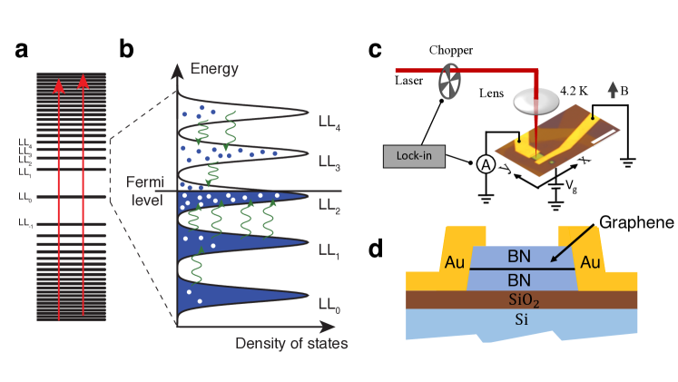
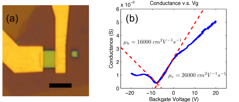
A schematic of our experimental setup and device structure are shown in Fig. 1(c),(d). An optical microscope image of the graphene sample (2.49 m by 3.87 m) is shown with metallic gold contacts on two sides. These two contacts are unbiased in photocurrent measurements. The exfoliated graphene layer is sandwiched between exfoliated boron nitride, and the structure is back-gated using the Si substrate (See Appendix for details). The carrier density (i.e. Fermi energy) in the sample can be tuned by changing the back gate voltage Novoselov et al. (2004); Wang et al. (2008). The photocurrent data are taken at 4.2 K predominantly with an out-of-plane magnetic field of 4 T. Additional data at a magnetic field of 9 T magnetic field is shown in the Appendix. Except where noted, the light source is a laser tuned to 930 nm with a power fixed at 10 W. The laser spot size on the sample is 1.8 m.
Fig. 1(a),(b) schematically show the Landau level quantization of the graphene density of states and the laser excitation. In the integer quantum Hall regime, the optically allowed interband transitions are between Landau levels such that, where are the respective principle quantum numbers, and are negative below and positive above the Dirac point Sadowski et al. (2006); Jiang et al. (2007). However, in the near infrared energy range, the transition energies between Landau levels are not expected to be discrete because of Landau level broadening at these high energies, in particular due to the sample impurity and disorder effects Funk et al. (2015). We measure the photocurrent between unbiased ohmic contacts (Fig. 2(a)) Nazin et al. (2010); Masubuchi et al. (2013); Cao et al. (2016); Sonntag et al. (2017). By sweeping the laser wavelength in the ranges 0.9 to 1 m () and 1.9 to 2.0 m () at 9 T we find that the photocurrent is unchanged for all the wavelengths in each range, confirming the absence of well-defined Landau levels in this energy range. For a laser power of 10 W and at a magnetic field above 2 T, the maximum of photocurrent we measured is 30 nA. This value corresponds to approximately 10 % of the carriers generated by the laser (see Appendix). Only small photocurrents ( nA) are measured at zero magnetic field (see Appendix).
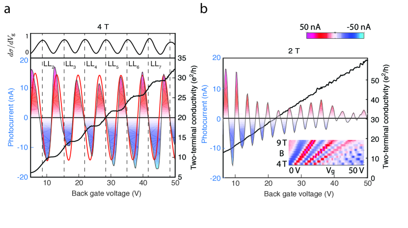
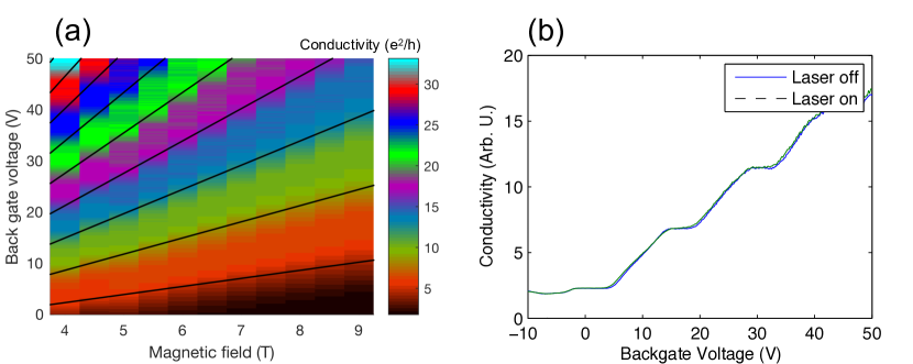
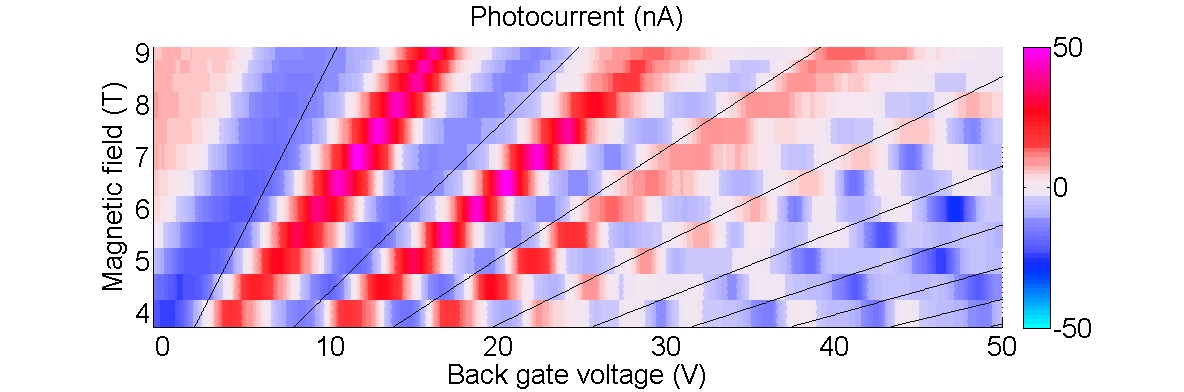
To demonstrate that the photocurrent reveals the integer quantum Hall physics, we measure the photocurrent generated by the laser while sweeping the back gate voltage. Fig. 2(a) shows that the photocurrent oscillates as a function of the back gate voltage under a magnetic field of 4 T when the laser is 1.5 m away from the sample center. To show that the photocurrent oscillations are correlated with the Landau levels, we perform a two-terminal conductance measurement, as shown in Fig. 2a (black line). The conductance measurement exhibits integer quantum Hall plateaus Novoselov et al. (2005); Zhang et al. (2005) correlated with photocurrent oscillations. In particular, away from the Dirac point (for Landau levels ), the zeros of the photocurrent correspond to both the middle of each plateau and the middle of the transition between two plateaus. These points corresponds to full filling and half filling of Landau levels, respectively. An alternative way to connect filling factors and changes in photocurrent polarity is to plot the derivative of conductance measurement with respect to the back gate voltage , as shown in the upper panel of Fig. 2(a). In inserts in Fig. 2(b) and the Appendix Fig. 7, we also change the magnetic field and observe the same correlation between photocurrent and conductance measurements.
The photocurrent measurements are more sensitive in the low magnetic field regime than the two-terminal transport measurements. Fig. 2(b) shows the two-terminal conductivity and the photocurrent as a function of the back gate voltage, at a low magnetic field of 2 T. While the quantum Hall plateaus are not visible in the two-terminal measurement, the oscillations of the photocurrent are pronounced. One explanation is that the two-terminal transport measurement evaluates the sum of edge state conductance, while the photocurrent is the difference of two components currents (electrons and holes) making it more sensitive.
The photocurrent oscillations track the back gate voltage, indicating that the physics is influenced by the density of states near the Fermi level. However, the polarity of the current indicates that the contributing carriers are not at the Fermi level, but are non-equilibrium (hot) carriers. To further clarify this, we set the Fermi level slightly above half-filling of a Landau level, as illustrated in Fig. 1(b). In this regime, the number of available hole states in the Landau level is larger than that of the electron states. If we assume relaxation to available Fermi-level states is fast Plochocka et al. , then the number of holes that relaxed to the Fermi level is larger than that of the electrons. The transport of the carriers near the Fermi level would be hole dominated, while hot carrier transport would be electron dominated. In this case, the measured polarity of the photocurrent indicates that the transport to the contact is dominated by electrons. Thus, we conclude that the photocurrent is due to hot carriers, and not the carriers in the vicinity of the Fermi level, as would be the case for local heating.
We develop a model to explain the observed dependence of the photocurrent on the back gate voltage. In the model, photocurrents are due to hot carriers, as described above. We further assume that the photocurrent is dominated by the edge physics, and carriers reach the edges with a probability set by the laser spot location relative to the sample edges. The validity of this is discussed later.
To determine the direction of the edge current due to electrons and holes, we now discuss their behavior in the presence of the confining edge potential. By solving the Schrödinger equation in the Landau gauge , the system is translationally invariant along the -axis, and the energy spectrum as a function of the confinement potential is where is the band index, for conduction band and for valence band. is the Fermi velocity, is the magnetic length, is the Landau level index, is the carrier charge. Therefore, the group velocity in the y-direction is given by:
| (1) |
where is the edge state momentum in the y-direction. This equation determines the direction of electron and hole edge transport. For example, above the Dirac point, since the confining potential and the charge have opposite signs for electrons and holes, their group velocities are in the same direction, and their currents are in opposite direction, as shown in Fig. 3(b),(c).
Using this picture, we explain the oscillation of the photocurrent with the back gate voltage. At both half- and integer-filling of Landau levels, the number of available electron and hole states are equal in the vicinity of the Fermi level. This makes the number of hot electrons and holes equal, leading to a net zero edge current. By moving away from half- and integer-filling factors, the number of available electron and holes are no longer equal; thus, the photocurrent becomes nonzero, and makes a full oscillation per Landau Level.
In our numerical model, we sum over thermally occupied edge channels, for both electrons and holes, and we evaluate the resulting photocurrent. The details of the model are described in the Appendix. The result of this model is presented as a red curve in Fig. 2(a), which qualitatively agrees with our observation. Specifically, the signal oscillates with the back gate voltage, changing polarity twice per Landau level, at half- and integer-fillings. Note that the discrepancy between photocurrent amplitudes of the two polarities on the same edge can be explained by the bulk mobility difference of electrons and holes, which is included in our numerical model.
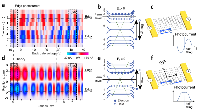
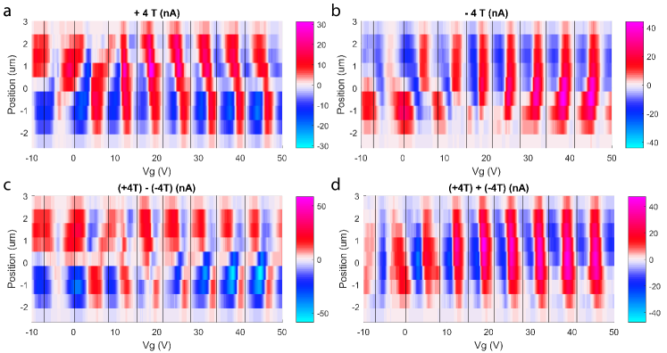
To study the spatial dependence of the photocurrent, we scan the laser spot position parallel to the contacts, i.e. along x-direction (see Fig. 1(c)). The photocurrent consists of two current components: one is diffusive, directly to the ohmic contacts while the other reaches the contacts through the edge states Song and Levitov (2014). The purely diffusive component is symmetric with the B-field. The second component is chiral, and thus antisymmetric with the B-field. Thus, the two components can be separated by taking the sum and difference of photocurrents, for +B and -B fields Cao et al. (2016). Fig. 3(a) shows the isolated magnetic-field dependent photocurrent as a function of and laser spot position (the original B data is in Fig. 9 in the Appendix). We observe that the photocurrent difference is weak in the middle of the sample (position 0 m), compared to the edges. Moreover, the photocurrent polarities have opposite sign on the two edges of the sample. These two observations confirm that the difference of photocurrents, for + B and - B fields is due to the diffusion of carriers to the nearest edge state, after which they are transported to the contacts via the edge states. We note, in contrast to transport measurements where the edge current balance is broken by the application of an electric field, here, the current imbalance is due to fact that the laser spot is off-centered on the sample.
We observe that regardless of the excitation position of the laser in x-direction, when the Fermi level is above the Dirac point (), the photocurrent changes polarity twice per Landau Level, as explained above. However, when the Fermi level is in the vicinity of the Dirac point , the photocurrent does not change polarity, as we sweep through the zeroth Landau level. This observation is also described by our model. Specifically, when the Fermi level is in the vicinity of the zeroth Landau level, electrons are above the Dirac point while holes are below the Dirac point leading to the same confining potential sign for electrons and holes. According to Eqn. 1, the group velocity is opposite for electrons and holes in this case, and their respective currents are therefore in the same direction, Fig. 3(e),(f). Thus, by sweeping through the zeroth Landau level, the photocurrent shows a maximum and does not change sign. A simulation based on our model is shown in Fig. 3(d) which qualitatively agrees with the experimental result. The simulation shows a small double peak at the zeroth Landau level due to fast electron-hole recombination, however this double peak is not resolved in the experiment.
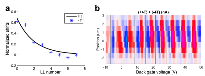
We note our observation can not be explained by local heating (the photo-Nernst effect) which was previously discussed in Ref. Cao et al. (2016) and our theoretical model differs from it. Broadly summarizing, the Nernst effect yields a current that is related to two adjacent regions at different equilibrium temperatures. If the graphene sample is heated, the transport is modulated as the Fermi-level occupation is locally altered Zhang et al. (2005); Zuev et al. (2009). In contrast, in our model, the electron and hole populations are in nonequilibrium distributions. The transport is due to hot carriers created by the laser, with a spot size on the order of the sample size, and we see no evidence of laser heating when comparing two-terminal transport measurements with and without the laser. Furthermore, details of our photocurrent measurement are consistent with our hot carrier transport model. In particular, as is shown in Fig. 2(a) and Fig. 3(a), the zeros of the photocurrent for Landau levels gradually shift away from the half-fillings for decreasing . As seen in Fig. 4(a), this shift can be fit with an exponential suggesting the hot carrier distribution is present through several Landau levels. We also evaluate the sum of the photocurrent measured for +B and -B fields, and we observe oscillations with a relative high amplitude ( 40 nA). This is shown in Fig. 4(b), and we note this observation cannot be explained in the photo-Nernst model where no oscillations are expected Cao et al. (2016). Finally, measurement at 4 T shows that oscillation amplitudes remain constant through several Landau levels–beyond a back gate voltage of 50 V (Fig. 2(a)), while data and theory for the Nernst effect suggest the photocurrent decays quickly away from the charge neutrality point.
In summary, we present optical probing of a monolayer graphene in the quantum Hall regime through the generation of non-equilibrium carriers. Our photocurrent measurement provides deeper insights into the carrier transport behavior in the quantum Hall regime, in particular, their chirality above and below the Dirac point. Such optical probing permits the study of the quantum Hall states in an intermediate length-scale regime, which could be applied to other 2D material systems Ju et al. (2017); Ma et al. (2017); Kastl et al. (2015); Arikawa et al. (2017). In addition, this work will contribute to developing novel applications of semiconductor materials, such as engineering the Peltier coefficient Skinner and Fu (2018).
We acknowledge support by the NSF Physics Frontier center at the JQI, PFC@JQI. We also acknowledge fruitful discussions with Xiao Li, Wade DeGottardi and Fereshte Ghahari.
*
Appendix A Sample preparation and transport measurements
A.1 Sample fabrication
Highly oriented pyrolytic graphite (HOPG) graphene and hexagonal boron nitride (hBN) are exfoliated using Scotch tape at ambient environment onto SiO2/Si substrate that is cleaned in Pirana solution followed by O2 plasma cleaning Wang et al. (2013). The top hBN is picked up by a stacking of glass (0.25 mm thick, on top), PDMS (1 mm thick) and PPC (spin coated at 3000 RPM onto PDMS). PDMS was O2 plasma treated before spin coating to promote adhesion of PPC. The pick up is done at 40 C using a home made transfer stage. Same procedure is used to pick up subsequent graphene and bottom hBN. The stacking is then pressed against the target substrate (SiO2/Si) which is heated to 90 C. The glass/PDMS/PPC is then detached from the target substrate. The sample is then immersed in acetone overnight to remove residual PPC. EBL (30 keV) is used to define sample shape, using PMMA A4 as mask. The etching is done in in the plasma of O2 (10 sccm) and SF6 (40 sccm) at a chamber pressure of 200 mtorr for about 1 min (etching rate is 20 nm/min). A second EBL is used to place contacts (Cr (5 nm)/Pd (10 nm)/Au (70 nm)) at the edges of the device. The device is then wire bonded using Au wires (25 um thick). The doped Si substrate is used as a back gate to control the carrier density in graphene.
An optical microscope image of the fabricated sample is shown in Fig. 5(a). The sample size is 2.49 m by 3.87 m. Measurements on other samples confirm the presented results. We estimate the contact resistance by calculating the sample resistance with the measured mobility. The difference between the measured resistance and the calculation is the contact resistance.
A.2 Transport measurement under magnetic field
Two-terminal transport measurements are conducted under various magnetic fields. Plateaus of conductance due to Landau level quantization can be readily seen, as shown in Fig. 6 (a). In the transport measurement, an AC current of 1 A at 13 Hz is injected through the drain and source contacts. A lock-in amplifier is locked at 13 Hz to measure the voltage drop between the drain and source. The conductance is obtained by taking the division between the 1 A current and the voltage drop measured. During the measurement, a perpendicular static magnetic field is applied while the gate voltage is tuned to change the carrier density in the sample.
We compare the two-terminal transport measurements with laser on and off. We use an OPO laser with wavelength about 2 m to excite the sample and a transport measurement is conducted. We turn off the laser and conduct another transport measurement. The comparison of the two transport measurements is shown in Fig. 6(b). The two measurements overlap with each other very well showing no sign of heating.
Appendix B The photocurrent measurement
We use near-infrared laser to excite electrons from below the Dirac point to above the Dirac point and measure the resulting photocurrent. We have repeated the photocurrent measurements on several samples.
B.1 The photocurrent measurement setup
The sample, at 4.2 K, is mounted on x, y, z translation stages with relative position-readout. A free-space confocal microscope system is used to image the pump laser on the sample. The laser is a CW Ti:Sapphire laser of 10 W with a fixed wavelength of 930 nm. This laser is chopped with a optical chopper at a frequency of 308 Hz.
The photocurrent is measured without any external bias. A lock-in amplifier, locked to the laser, is used to measure the laser generated photocurrent between the source and drain contacts. During the measurement, both the perpendicular magnetic field and the backgate voltage are tuned. The resulting photocurrent as a function of magnetic field and backgate voltage shows a similar fan diagram as the transport measurement, as shown in Fig. 7.
B.2 Photocurrent generation efficiency
The 930 nm CW Ti:Sapphire laser corresponds to =1.33 . The laser power applied on the surface of the sample is =10 . The number of photons per second in the pump laser is . If we assume the absorption rate of a monolayer graphene is about 2% Wang et al. (2008) and to first order due only to particle-hole generation, the particle-hole generation rate, is then about .
The photocurrent amplitude we measure is in the regime of several tens of , which is equivalent to a rate of charged particles transport of . Comparing and , we find that about 10% of the excited particles and holes are measured in photocurrent.
B.3 Power dependence measurement
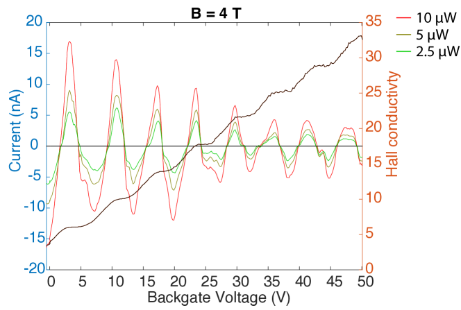
The power dependence measurement shows that the laser power of 10 W is in the linear response regime of the graphene photocurrent. Here, as an example, we show photocurrent oscillation as a function of back gate voltage for three laser powers: 2.5 W, 5 W, 10 W, where it can be seen that doubling of the laser power results in doubling of the oscillation amplitude.
The linear response regime is also predicted by a simple, order of magnitude argument. The excited carrier lifetime has been measured Plochocka et al. , leading to a recombination rate between . This exceeds by at least an order of magnitude the carrier generation rate (), and supports that the carrier generation at the laser power is in the linear response regime.
B.4 Laser spot size characterization
The laser spot size is characterized by reflection from the gold contacts. The reflected light from the sample is collected through an optical fiber and measured. When the laser spot is on the gold contacts, the reflected power increases due to a higher reflection of gold as compared to the heterostructure. By moving the laser from graphene to a gold contact, the profile of the laser spot is mapped out. Our measurement shows the laser spot has a full-width half maximum of 1.8 m.
B.5 Photocurrent maps at magnetic fields of 4 T, 9 T
We map out the photocurrent as a function of the position parallel to the contacts by moving the laser spot from edge to edge (along x-direction in Fig. 1(c) in the main text), as shown in Fig. 9(a) for 4 T and Fig. 9(b) for -4 T. The laser is fixed at 10 W and 930 nm. During the position scan, the laser spot is fixed in the center of the sample along y direction, perpendular to the two contacts. We observe photocurrent oscillations as a function of back gate voltage with polarity changes according to the Landau quantization. As explained in the main text, the photocurrent consists of diffusive current directly to the ohmic contacts and the edge state transport current. The polarity also switches in the center of the sample because now transport from the opposite edge begins to dominate.
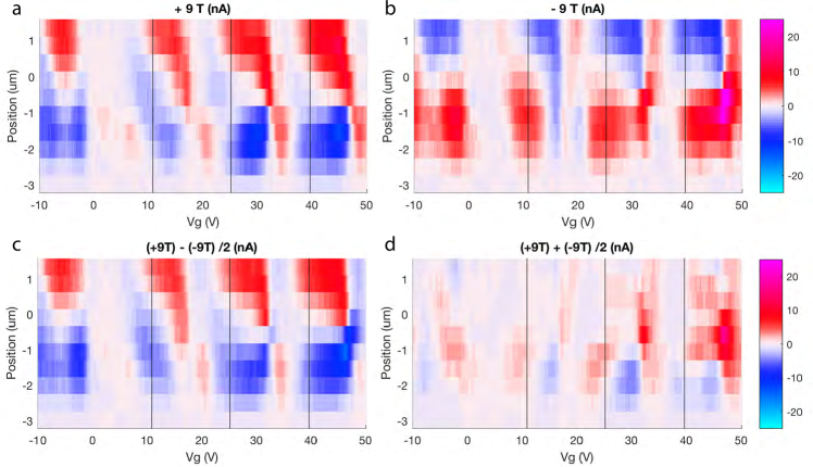
To obtain the edge state and bulk contribution, we sum over or subtract the T results Cao et al. (2016), as shown in Fig. 9(c),(d). We observe that the edge transport component of the photocurrent is weak when the laser is focused in the center compared to the edge, and the two edges have opposite polarities, Fig. 9(c). In contrast, the bulk transport part of the photocurrent is symmetric along the x-direction, Fig. 9(d). Similar measurements are done for T, as shown in Fig. 10.
Appendix C Photocurrent mechanism
The explanation of the photocurrent generation can be separated into two parts: A. Imbalanced relaxation of hot carriers. B. Chirality of edge states. These two mechanisms in combination results in the photocurrent that we observe in the experiments.
C.1 Imbalanced relaxation of hot carriers
The relaxations of electrons and holes are imbalanced when the Fermi level is not in the half-filling of a Landau level. The relaxation rate of hot carriers is determined by the number of available states. When the Fermi level is above the half-filling, the number of available states for electrons is smaller than the one for holes resulting in that the holes relax faster than electrons. In this regime, the number of hot electrons is greater than the number of hot holes. These hot electrons/holes distribute in multiple Landau levels above/below the Fermi level. The hot carriers dissipate to the nearest edge and give a hot-electron-dominate photocurrent. A similar mechanism is described in Nazin et al. (2010).
By sweeping the Fermi level through multiple Landau levels, the hot carrier type switches between electrons and holes multiple times, which manifests as the change of polarities of the measured photocurrent. However, the absolute type of the photocurrent’s polarity is determined by the transport direction of the hot carriers.
C.2 Chirality of edge states
Aside from deriving the chirality of edge states from the Schrödinger equation as introduced in the main text, we can also describe it with the Dirac equation Queisser and Schützhold (2013).
| (2) |
where is the two-atom basis wavefunction and we can assume is real and is imaginary. and are the Pauli matrices. is the Fermi velocity. We use the Landau gauge here . Because of the translation symmetry, we can separate variables as Then we can have equations,
| (3) |
The other set of solution can be obtained by substituting . The way to interpret the two solutions and is that is the electron or hole with energy (which can be positive or negative). Correspondingly is the hole or electron with energy Greiner et al. (2012).
The definition of the current Queisser and Schützhold (2013) is,
| (4) |
Here, is the carrier charge. Using eqn. (3), it is found that electron/hole can only flow in the y-direction,
| (5) |
For electron and hole on the same side of the Dirac point i.e. , the flow directions are the same for electron and hole, leading to opposite currents because of the opposite charge of electron and hole. For electron and hole separated by the Dirac point, i.e. , the flow directions are opposite, giving additive currents. The edge state chirality is independent of the type of edge, zigzag or armchair Abanin et al. (2007).
The edge states transport plays a key role in the photocurrent generation. Hot electrons and holes diffuse to edge states and contribute to the photocurrent. The chirality of edge states, thus, determine the polarity of the photocurrent. In the high Landau level regime where all the hot electrons and hot holes are on the same side of the Dirac point, we see polarity change of photocurrent when the backgate voltage is at the half fillings of one Landau levels, as shown in the dashed box in Fig. 3(a) in the main text.
In the zeroth Landau level, the case is different. When electron and hole are separated by the Dirac point, the edge states transport to opposite directions which leads to the photocurrent of the same polarity, as is shown in the derivation above. Thus, at the zeroth Landau level, we see peaks of photocurrent which centers at the Dirac point, as shown in the dashed box in Fig. 3(a) in the main text. When the Fermi level moves away from the Dirac point to the high Landau level regime, the half-filling gradually shifts to coincide with the zeros of the photocurrent. This is due to the distribution of hot carriers through multiple Landau levels as explained above.
The mobility difference of electrons and holes results in the different photocurrent amplitudes of two polarities. We include this fact in our simulation.
Appendix D Model
In our model, photocurrents are due to hot carriers which have not relaxed back to the Fermi energy. Relaxation rates () for electrons (holes) are determined by the density of states within a small strip above (below) the Fermi level, given through the gate voltage . The Landau levels are centered around integer multiples of , the voltage difference between a filled and an empty Landau level. Note that the relation between Fermi energy and gate voltage is , leading to an equidistant spacing of Landau levels with respect to gate voltage. The number of states is assumed to be distributed according to a Lorentzian of width , so for the density of states we may write . For our sample, we estimate , and we consider a carrier as relaxed if the corresponding gate voltage is within . Thus, for the relaxation rates, we write:
| (6) | ||||
| (7) |
In these expressions we have introduced a parameter for the time scale of the relaxation process. The probability that an electron (e) or hole (h) contributes to the photocurrent, , will depend on its relaxation rate , and another time scale, , the time which is needed for the carrier to reach the edge. We have:
| (8) |
From this expression, we determine the net photocurrent signal by considering the direction of edge transport. It is given by the chirality of the Landau level and the geometric edge which carries the charge. As argued in Eq. (1) of the main text, the chirality of a Landau level changes with the sign of its energy, and also opposite geometric edges have opposite direction of transport.
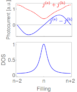
For concreteness, let us now assume a positive Fermi energy. For the moment, let us also assume that only one geometric edge is involved in transport. With these assumptions, the transport direction for the electrons is fixed, but holes appear either with positive or negative energy, leading to transport either along with the electrons or in opposite direction. Thus, knowledge of the energy distribution of hot holes is needed in order to determine the photocurrent signal. Without that knowledge, we may still consider the two limiting cases: One limiting case occurs when the Fermi level approaches the Dirac point, such that the vast majority of holes must be at negative energy. Then, electrons and holes are counter-propagating, and due to their opposite charges their photocurrent contributions add up: . This results in a strong signal which does not display a polarity change along , see red curve in upper panel of Fig. 11.
Conversely, in the other limiting case, the Fermi level is far from the Dirac point. Then, almost all holes have relaxed to positive energies, since the relaxation through highly excited empty levels is much faster than relaxation processes near the Fermi level. In this case, electrons and holes move along the same direction, and their contributions to the photocurrents point in opposite directions, . At the extrema of , the density of states is symmetric, and electron and hole contribution cancel each other. Thus, the polarity of the photocurrent changes between two Landau levels and at half-filled levels, see blue curve in upper panel of Fig. 11.
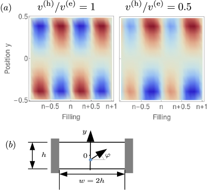
In the following, we will take into account the existence of two geometric edges. This becomes important when carriers are not excited in close vicinity to one edge. The photo-excited carriers are expected to drift in an arbitrary direction, and may reach any edge of the sample, or even one of the leads without going through an edge channel. Position of a carrier, and its drift direction (cf. Fig. 12(b)) define the distance to the edge. The drift time is given by , where is the drift velocity. Here, we assume different velocities for electrons and holes due to different mobilities. Substituting in Eq.(8) by these expressions, we obtain a photocurrent probability which depends not only on the Fermi level , but also on the position and the drift direction . To keep track of the polarity of the corresponding current, we also introduce a binary variable , where the sign is defined by the geometric edge which is reached by a drift from along .
In the two limiting cases with all carriers of one species having the same chirality, the photocurrent contribution of each carrier type is then given by
| (9) |
For example, sufficiently far away from the Dirac point, the total photocurrent signal will then be given by , as plotted in Fig. 12(a) for equal and unequal mobilities of electrons and holes ( and ). Drift velocities have been related to the relaxation time scale introduced in Eq. (6) by .
Finally, in order to model the full experimental data, we must take into account that holes (electrons) of any chirality co-exist when the Fermi energy is above (below) the Dirac point. Therefore, we introduce a Boltzmann weight, and set the gate voltage at the Dirac point to zero, . Then, the portion of electrons (holes) below (above) the Dirac point is assumed to be given by for (), with being a temperature-like parameter. For the total photocurrent signal we then write:
| (10) |
Our modeling in the main text, shown in Fig. 3(d), was obtained from Eq. (D) using the parameters . The laser beam size of full-width-half-maxium 1.8 is taken into the consideration by convolution. The little dip in the photocurrent intensity at the zeroth Landau level is due to the fast electron-hole recombination rate.
References
- Zhang et al. (2005) Y. B. Zhang, Y. W. Tan, Horst L Stormer, and Philip Kim, “Experimental observation of the quantum Hall effect and Berry’s phase in graphene,” Nature 438, 201–204 (2005).
- Novoselov et al. (2005) K S Novoselov, A K Geim, S V Morozov, D Jiang, M I Katsnelson, I V Grigorieva, S V Dubonos, and A A Firsov, “Two-dimensional gas of massless Dirac fermions in graphene,” Nature 438, 197–200 (2005).
- Geim and Novoselov (2007) A. K. Geim and K. S. Novoselov, “The rise of graphene,” Nature Mater. 6, 183–191 (2007).
- Orlita et al. (2011) M. Orlita, C. Faugeras, R. Grill, A. Wysmolek, W. Strupinski, C. Berger, W. A. De Heer, G. Martinez, and M. Potemski, “Carrier scattering from dynamical magnetoconductivity in quasineutral epitaxial graphene,” Phys. Rev. Lett. 107, 216603 (2011).
- Jiang et al. (2007) Z. Jiang, E. A. Henriksen, L. C. Tung, Y. J. Wang, M. E. Schwartz, M. Y. Han, P. Kim, and H. L. Stormer, “Infrared spectroscopy of landau levels of graphene,” Phys. Rev. Lett. 98, 197403 (2007).
- Chen et al. (2014) Zhi Guo Chen, Zhiwen Shi, Wei Yang, Xiaobo Lu, You Lai, Hugen Yan, Feng Wang, Guangyu Zhang, and Zhiqiang Li, “Observation of an intrinsic bandgap and landau level renormalization in graphene/boron-nitride heterostructures,” Nature Commun. 5, 4461 (2014).
- Sadowski et al. (2006) M. L. Sadowski, G. Martinez, M. Potemski, C. Berger, and W. A. De Heer, “Landau level spectroscopy of ultrathin graphite layers,” Phys. Rev. Lett. 97, 266405 (2006).
- Nazin et al. (2010) G Nazin, Y. Zhang, L Zhang, E. Sutter, and P Sutter, “Visualization of charge transport through Landau levels in graphene,” Nature Phys. 6, 870–874 (2010).
- Masubuchi et al. (2013) Satoru Masubuchi, Masahiro Onuki, Miho Arai, Takehiro Yamaguchi, Kenji Watanabe, Takashi Taniguchi, and Tomoki Machida, “Photovoltaic infrared photoresponse of the high-mobility graphene quantum Hall system due to cyclotron resonance,” Phys. Rev. B 88, 121402(R) (2013).
- Cao et al. (2016) Helin Cao, Grant Aivazian, Zaiyao Fei, Jason Ross, David H. Cobden, and Xiaodong Xu, “Photo-Nernst current in graphene,” Nature Phys. 12, 236–239 (2016).
- Wu et al. (2016) S. Wu, L. Wang, Y. Lai, W.-Y. Shan, G. Aivazian, X. Zhang, T. Taniguchi, K. Watanabe, D. Xiao, C. Dean, J. Hone, Z. Li, and X. Xu, “Multiple hot-carrier collection in photo-excited graphene Moire superlattices,” Science Advances 2, e1600002–e1600002 (2016).
- Sonntag et al. (2017) Jens Sonntag, Annika Kurzmann, Martin Geller, Friedemann Queisser, Axel Lorke, and Ralf Schützhold, “Giant magneto-photoelectric effect in suspended graphene,” New J. Phys. 19, 063028 (2017).
- Wendler et al. (2014) Florian Wendler, Andreas Knorr, and Ermin Malic, “Carrier multiplication in graphene under Landau quantization,” Nature Commun. 5, 3703 (2014).
- (14) P Plochocka, P Kossacki, A Golnik, T Kazimierczuk, C Berger, W A De Heer, and M Potemski, “Slowing hot-carrier relaxation in graphene using a magnetic field,” 10.1103/PhysRevB.80.245415.
- Rutter et al. (2007) G M Rutter, J N Crain, N P Guisinger, T Li, P N First, and J A Stroscio, “Scattering and Interference in Epitaxial Graphene,” Science 317, 219–222 (2007).
- Brar et al. (2007) Victor W. Brar, Yuanbo Zhang, Yossi Yayon, Taisuke Ohta, Jessica L. McChesney, Aaron Bostwick, Eli Rotenberg, Karsten Horn, and Michael F. Crommie, “Scanning tunneling spectroscopy of inhomogeneous electronic structure in monolayer and bilayer graphene on SiC,” Appl. Phys. Lett. 91, 122102 (2007).
- Hashimoto et al. (2008) K. Hashimoto, C. Sohrmann, J. Wiebe, T. Inaoka, F. Meier, Y. Hirayama, R. A. Römer, R. Wiesendanger, and M. Morgenstern, “Quantum hall transition in real space: From localized to extended states,” Phys. Rev. Lett. 101, 18–21 (2008).
- Ghahari et al. (2017) Fereshte Ghahari, Daniel Walkup, Christopher Gutiérrez, Joaquin F. Rodriguez-Nieva, Yue Zhao, Jonathan Wyrick, Fabian D Natterer, William G Cullen, Kenji Watanabe, Takashi Taniguchi, Leonid S Levitov, Nikolai B Zhitenev, and Joseph A Stroscio, “An on/off Berry phase switch in circular graphene resonators,” Science 356, 845–849 (2017).
- Halperin (1982) B. I. Halperin, “Quantized Hall conductance, current-carrying edge states, and the existence of extended states in a two-dimensional disordered potential,” Phys. Rev. B 25, 2185–2190 (1982).
- Das Sarma et al. (2011) S. Das Sarma, Shaffique Adam, E. H. Hwang, and Enrico Rossi, “Electronic transport in two-dimensional graphene,” Rev. Mod. Phys. 83, 407–470 (2011).
- Abanin et al. (2007) Dmitry A Abanin, Patrick A Lee, Leonid S Levitov, and A H Macdonald, “Charge and spin transport at the quantum Hall edge of graphene,” Solid State Commun. 143, 77–85 (2007).
- Queisser and Schützhold (2013) Friedemann Queisser and Ralf Schützhold, “Strong Magnetophotoelectric Effect in Folded Graphene,” Phys. Rev. Lett. 111, 046601 (2013).
- Hoppe et al. (2000) H. Hoppe, U. Zülicke, and Gerd Schön, “Andreev Reflection in Strong Magnetic Fields,” Phys. Rev. Lett. 84, 1804–1807 (2000).
- Amet et al. (2016) Francois Amet, Chung Ting Ke, Ivan V. Borzenets, Ying-Mei Wang, Keji Watanabe, Takashi Taniguchi, Russell S. Deacon, Michihisa Yamamoto, Yuriy Bomze, Seigo Tarucha, and Gleb Finkelstein, “Supercurrent in the quantum Hall regime,” Science 352, 966–969 (2016).
- Lee et al. (2017) Gil-Ho Lee, Ko-Fan Huang, Dmitri K. Efetov, Di S. Wei, Sean Hart, Takashi Taniguchi, Kenji Watanabe, Amir Yacoby, and Philip Kim, “Inducing superconducting correlation in quantum Hall edge states,” Nature Phys. 13, 693 (2017).
- Novoselov et al. (2004) K. S. Novoselov, A. K. Geim, S. V. Morozov, D. Jiang, Y. Zhang, S. V. Dubonos, I. V. Grigorieva, and A. A. Firsov, “Electric field in atomically thin carbon films,” Science 306, 666–669 (2004).
- Wang et al. (2008) Feng Wang, Yuanbo Zhang, Chuanshan Tian, Caglar Girit, Alex Zettl, Michael Crommie, and Y. Ron Shen, “Gate-variable optical transitions in graphene,” Science 320, 206–209 (2008).
- Funk et al. (2015) Hannah Funk, Andreas Knorr, Florian Wendler, and Ermin Malic, “Microscopic view on Landau level broadening mechanisms in graphene,” Phys. Rev. B 92, 205428 (2015).
- Song and Levitov (2014) Justin C.W. Song and Leonid S Levitov, “Shockley-Ramo theorem and long-range photocurrent response in gapless materials,” Phys. Rev. B 90, 075415 (2014).
- Zuev et al. (2009) Yuri M Zuev, Willy Chang, and Philip Kim, “Thermoelectric and magnetothermoelectric transport measurements of graphene,” Phys. Rev. Lett. 102, 096807 (2009).
- Ju et al. (2017) Long Ju, Lei Wang, Ting Cao, Takashi Taniguchi, Kenji Watanabe, Steven G. Louie, Farhan Rana, Jiwoong Park, James Hone, Feng Wang, and Paul L. McEuen, “Tunable excitons in bilayer graphene,” Science 358, 907–910 (2017).
- Ma et al. (2017) Qiong Ma, Su Yang Xu, Ching Kit Chan, Cheng Long Zhang, Guoqing Chang, Yuxuan Lin, Weiwei Xie, Tomás Palacios, Hsin Lin, Shuang Jia, Patrick A. Lee, Pablo Jarillo-Herrero, and Nuh Gedik, “Direct optical detection of Weyl fermion chirality in a topological semimetal,” Nature Phys. 13, 842–847 (2017).
- Kastl et al. (2015) C. Kastl, M. Stallhofer, D. Schuh, W. Wegscheider, and A. W. Holleitner, “Optoelectronic transport through quantum Hall edge states,” New J. Phys. 17, 023007 (2015).
- Arikawa et al. (2017) T. Arikawa, K. Hyodo, Y. Kadoya, and K. Tanaka, “Light-induced electron localization in a quantum Hall system,” Nature Phys. 13, 688–692 (2017).
- Skinner and Fu (2018) Brian Skinner and Liang Fu, “Large, nonsaturating thermopower in a quantizing magnetic field,” Science Advances 4, 1–7 (2018).
- Wang et al. (2013) L. Wang, I. Meric, P. Y. Huang, Q. Gao, Y. Gao, H. Tran, T. Taniguchi, K. Watanabe, L. M. Campos, D. A. Muller, J. Guo, P. Kim, J. Hone, K. L. Shepard, and C. R. Dean, “One-dimensional electrical contact to a two-dimensional material,” Science 342, 614–617 (2013).
- Greiner et al. (2012) W. Greiner, B. Müller, and J. Rafelski, Quantum Electrodynamics of Strong Fields: With an Introduction into Modern Relativistic Quantum Mechanics, Theoretical and Mathematical Physics (Springer Berlin Heidelberg, 2012).