Valley-Engineering Mobilities in 2D Materials
Abstract
Two-dimensional materials are emerging as a promising platform for ultrathin channels in field-effect transistors. To this aim, novel high-mobility semiconductors need to be found or engineered. While extrinsic mechanisms can in general be minimized by improving fabrication processes, the suppression of intrinsic scattering (driven e.g. by electron-phonon interactions) requires to modify the electronic or vibrational properties of the material. Since intervalley scattering critically affects mobilities, a powerful approach to enhance transport performance relies on engineering the valley structure. We show here the power of this strategy using uniaxial strain to lift degeneracies and suppress scattering into entire valleys, dramatically improving performance. This is shown in detail for arsenene, where a strain stops scattering into 4 of the 6 valleys, and leads to a increase in mobility. The mechanism is general and can be applied to many other materials, including in particular the isostructural antimonene and blue phosphorene.
In the last decade, two-dimensional (2D) materials have shown a wealth of novel physical phenomena, and manifold possible technological applications. Their ultimate thinness is particularly suitable for applications in conventional and flexible electronics Wang2012 ; Fiori2014 ; Chhowalla2016 ; Wang2014 ; Das2014 ; Akinwande2014 , where 2D semiconductors could be exploited as channels in field-effect transistors. An essential ingredient to boost performance of both logical and radio-frequency devices is a large carrier mobility. Up to now, the largest room-temperature mobility in 2D materials has been reported in grapheneChen2008 ; Dean2010 ; Efetov2010 ; Mayorov2011 ; Wang2013Nov , with optimal results in finite-frequency applicationsSchwierz2010 ; Grigorenko2012 ; Tassin2013 . Nonetheless, the absence of an energy gap prevents its use in logical devices. Other well-known 2D materials, such as transition metal dichalcogenides (TMD), show large on-off ratiosYoon2011 ; Radisavljevic2011 but display relatively poor carrier mobilitiesRadisavljevic2011 ; Allein2014 ; Jo2014 .
There is thus a pressing need to find 2D semiconductors with a finite band gap and, at the same time, high conductivity. To design or discover such materials one must minimize the scattering processes degrading electrical transport. Considering that the quality of samples can typically be improved systematically to suppress external scattering sources, such as impurities, design strategies should focus on maximizing intrinsic performance. In this respect, particular attention can be devoted to electron-phonon interactions, as phonons play a dominant role in limiting the intrinsic mobility of a material, especially at room temperature. In particular, the presence of multiple valleys within an energy range compatible with phonon frequencies leads to plentiful phonon-assisted intervalley scattering, that has detrimental effects on mobility. Indeed, even if this is not the only scattering mechanism present, we have recently shown Sohier2018 that intervalley electron-phonon coupling is large in well-known 2D semiconductors, to the point that there is a strong correlation between the number of valleys and the intrinsic mobility. This suggests a potential strategy to enhance electronic performance by engineering the valley structure to suppress intervalley electron-phonon scattering.
To achieve this goal, the extreme sensitivity of 2D materials to external manipulations can be beneficial, as it allows to easily tune electronic properties. As an example, 2D materials can be easily stretched, and it has been shown that strain plays an important role in determining the electronic and optical properties of 2D materialsRoldan2015 ; Mohiuddin2009 . For instance, strain fields open a gap in graphene on BN San-Jose2014 ; Jung2015 , change the gap from direct to indirect in antimonene Kripalani2018 or TMDsSteinhoff2015 , allow the manipulation of spin and valley transport Lee2017a ; Ma2016 , and reduce the band gap of TMDsShen2016 .
Here we explore the strong dependence of mobility on valley structure, and showcase that using strain is a very viable way to engineer the valley structure of 2D materials, leading to remarkable improvements in conductivity. We examine first arseneneZhang2015 ; Shah2018 ; BeladiMousavi2019 as a prototypical example, owing to its six-fold multivalley conduction bands, and show that a relatively small uniaxial strain is sufficient to break the six-fold symmetry and push four of these arsenene valleys high enough in energy to effectively suppress all the corresponding intervalley scattering processes, in turn greatly enhancing electron mobility. This effect is more general than in MoS2 Ge2014 (where it is very specific to the different character of inequivalent valleys and their behaviour under biaxial strain) and much larger than in conventional 3D multivalley semiconductorsSun2007 ; Takagi2008 ; Yu2008 ; Chu2009 ; Xu2012 ; Vogelsang1992 ; Vogelsang1993 ; Takagi1996 ; Rahman2005 ; Uchida2005 , such as silicon and germanium, with an enhancement factor that will be shown to be, for arsenene, of the order of 600%.
We stress that what is suggested here is at variance with recent theoretical studies that have proposed strain as a way to enhance mobility in various 2D materialsYu2016 ; Aierken2016 ; Shao2017 ; Xu2017 ; Phuc2018 ; Fang2019 ; Liu2015 ; Priydarshi2018 ; Xie2019 . These studies neglect intervalley scattering and consider the effect of strain on effective masses and, partially, on the intravalley scattering. Moreover, most rely on an acoustic-deformation-potential approximationTakagi1994 to compute mobilities, which seldom provides quantitative realistic predictions. Here, instead, we adopt an accurate and systematic approach to compute phonon-limited mobilities Giustino2017 that combines Boltzmann transport Ziman ; Grimvall with band and momentum-resolved scattering amplitudes obtained within density-functional perturbation theory Baroni (DFPT) in a framework that accounts for reduced dimensionality and field-effect dopingSohier2017 ; Sohier2018 . The strength of the approach is to provide a full and detailed picture of electron-phonon scattering by explicitly computing all possible phonon-mediated transitions, with a predictive power that can provide quantitative agreement with experimentsPark2014 ; Sohier2014a .
While we perform here an in depth study of arsenene (a monolayer of arsenic atoms forming a buckled hexagonal honeycomb structure) as a reference system, similar results can be expected for other group-V buckled monolayers, or other multivalley 2D materials. In the Supporting Information it is shown that the same features are also present in antimonene Ji2016 and blue phosphorene Zhang2018 . In addition, a search on our database of 2D materials Mounet2018 revealed that up to one third of semiconductors have degenerate multivalley electronic structures at the conduction or valence band edges, and could thus be valley-engineered. Also, although strain is very effective in modifying the valley structure of 2D materials, other mechanisms could be put forward to achieve the same scope (e.g. via stacking, substrate choice, functionalization). We thus stress that what we propose is more general than the specific compound (arsenene) and mechanism (strain) that we consider to exemplify the strategy of valley-engineering the mobility of 2D materials.
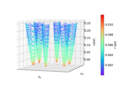
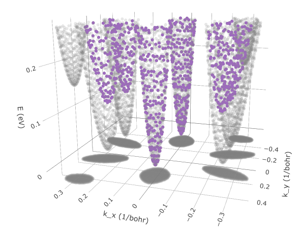
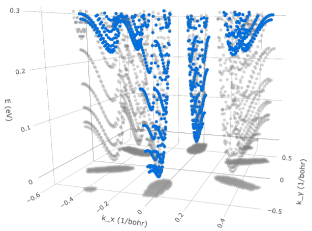
In the following, the zig-zag (armchair) direction is aligned with the () axis. For transport purposes, the conduction band of arsenene can be considered as consisting of six equivalent anisotropic valleys along the M lines, as shown in Fig. 2. Indeed, the next low-energy conduction band minima occur at least eV above the bottom of those valleys. We consider all electronic states up to eV above the bottom of the conduction band, and we have verified that this is enough to include all relevant states for transport for the doping levels and temperatures (up to 350 K) considered in this work.
Despite the anisotropy of each individual valley manifest in Fig. 2, the total mobility of arsenene is isotropic because of the hexagonal symmetry of the system. This has been shown both analyticallyPizzi2016a and numericallySohier2018 , and is expected from general symmetry considerationsNye . For completeness and clarity, we summarize here a general derivation that will be useful to elucidate transport properties under the application of strain. The total conductivity is a sum of contributions from each valley:
| (1) |
where is the index running over the six valleys (we choose the reference valley as the one in the direction, so that its principal directions simply coincide with the Cartesian axes), is the electron charge, are the band velocities, are the dependent scattering times, is the equilibrium Fermi–Dirac distribution, is a unit vector in the direction of the applied electric field, and the integral is over the area around each valley where is significantly different from zero. The contributions from each valley are related to each other by symmetry. Indeed, all valleys can be obtained by rotating the reference valley by angles . Eigenenergies and scattering times are invariant under these operations, and only the projection of the velocity on the electric field direction changes. We can thus obtain the conductivity equivalently by carrying out the integral in the reference valley () and rotating the electric field to add up the contribution of all valleys:
| (2) |
where , with giving the direction of the applied electric field.
By expanding the squared scalar product and noting that the corresponding cross product vanishes because of the mirror symmetry with respect to the M lines, we get:
| (3) | ||||
| (4) |
where the conductivity in the () direction for the reference valley will be denoted with the (or ) subscript because it corresponds to the high (or low) velocity and thus indicates the direction with the high (or low) conductivity. Summing up for yields:
| (5) |
independently of the direction of the field, proving that, even though the conductivity of a single valley is anisotropic (), the overall conductivity of the material is indeed isotropic Nye .
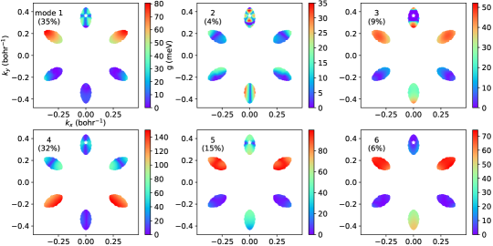
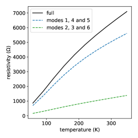
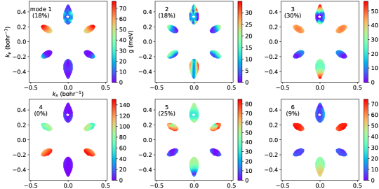
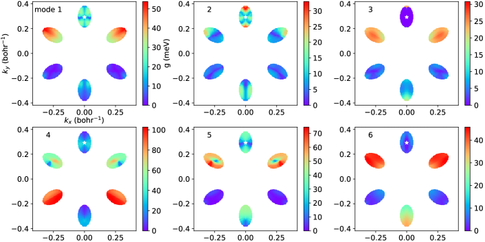
A detailed analysis of electron-phonon scattering in arsenene can help us reveal the strength of intervalley scattering and which intra- and intervalley couplings play the largest role in inhibiting transport performance. In particular, we show in Fig. 2 the electron-phonon couplings (EPCs) for each phonon mode and their contribution to transport. We can see that 80% of the resistivity comes from scattering with modes associated with strong intervalley EPCs, corresponding to phonon momenta and . Considering an initial state in the reference valley, these modes correspond to transitions to valleys rotated by .
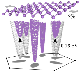
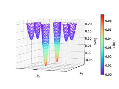
It would thus be beneficial to suppress scattering to these valleys to enhance the electronic transport performance. Valleys in different directions have the same energy because of the 3-fold and inversion symmetries of the crystal. Breaking these symmetries removes the degeneracy and allows for the emergence of an energy difference between valleys. If this energy difference is large enough, valleys that are shifted up in energy become out of reach, i.e., electrons cannot be scattered into them via a phonon-mediated event. In this respect, it is important to keep in mind that, under the assumption of constant charge (see below), the remaining valleys contain more carriers, so that the Fermi energy is also shifted up in energy with respect to the bottom of the conduction band, which is fully accounted for in our calculations and discussed in details later. As a consequence, in order to fully suppress intervalley scattering, the shift in energy of the valleys should be large enough so that the bottom of the valleys is higher than the (new) Fermi level by at least the largest phonon energy (relatively low in arsenene, eV for the relevant phonons involved in intervalley scattering events) plus the thermal energy (also eV at 300 K).
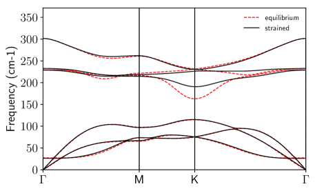
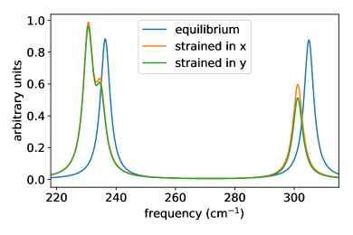
We consider a strain along the (zig-zag) direction that pushes all the valleys that are not on the axis (4 out of 6, see also Fig. 4) high in energy with respect to the band edge, as opposed to a strain along the (armchair) direction that would instead shift only two valleys to higher energy111According to Ref. Pizzi2016a, the deformation potential of the conduction valleys is positive in the longitudinal direction and negative in the transverse direction, so that with a strain along the direction two valleys (the ones with longitudinal direction along ) are pushed down and the other four are pushed up, while the opposite is true (two up and four down) for strain along the direction.. In particular, we find that a uniaxial strain222in practice, depending on the experimental setup, such an uniaxial stretch might be accompanied by a compression in the perpendicular direction. This is not included in our simulations, but we checked that the effects of a full relaxation in the perpendicular direction are minimal. induces a largely sufficient energy shift of eV. Such a strain is readily within the possibilities of experimental realization Mohiuddin2009 ; Huang2009 and can be indirectly monitored through its effects on arsenene’s Raman spectrum, in particular through the splitting of the Eg mode (see predicted Raman spectra under strain and their polarisation dependence in Supporting Information F). In antimonene and blue phosphorene, the same strain shifts the same valleys by and eV, respectively (also see Supporting Information D and E). Note that according to Ref. Pizzi2016a, (supplementary figure 5), one can roughly assume a linear variation of the shifts with strain.
We simulate equilibrium and strained arsenene in the appropriate two-dimensional frameworkSohier2017 by truncating the long-range Coulomb potential in the non-periodic direction. This ensures that no spurious interactions exist between the periodic images, yielding in particular the correct 2D screening of the electron-phonon coupling. We also use a symmetric double-gate geometrySohier2017 to induce a charge density of cm-2. The Brillouin zone is sampled with a Monkhorst-Pack grid and we use the SSSP Accuracy (version 0.7) pseudopotential libraryPrandini2018 with the associated cutoffs. We note that the density of states (DOS) at the bottom of the conduction band is approximately three times smaller for strained arsenene, since two thirds of the valleys have been shifted up. Thus, the two remaining low-lying valleys fill up three times faster as a function of the doping charge. The same density of free carriers is considered in both the strained and unstrained cases, under the assumption that the gate capacitance is mainly controlled by geometric effects and that the reference potential of the material is almost unaffected, so that the density is completely controlled by the gate potential and thus stays constant under strain. The reference value of density ( cm-2) is then chosen so that the shifted valleys in the strained case are not occupied, while the valleys in the pristine case are still significantly filled.
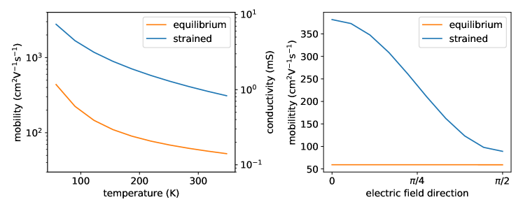
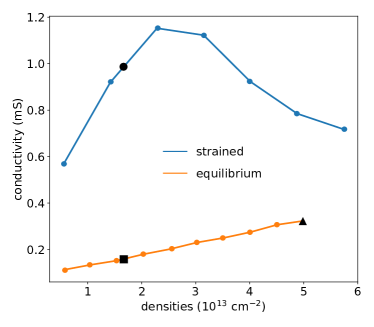
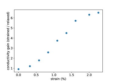
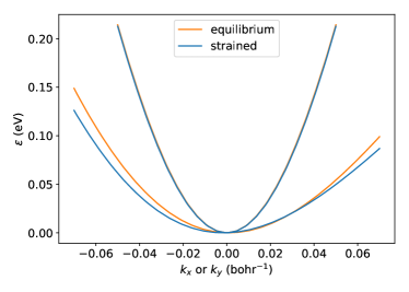
Mobilities are computed with the method described in Ref. Sohier2018, , which is based on direct calculation of phonons and EPCs within DFPT in the aforementioned framework including the proper boundary conditions and explicit gate-induced doping. The Boltzmann transport equation is solved numerically with an exact integration method and different levels of momentum sampling, from a relatively coarse -point grid used for DFPT calculations to a much finer -point grid for eigenenergies and velocities. The transport properties that we computed for equilibrium and strained arsenene are compared in Fig. 3. For a strain, we observe a significant improvement of the transport properties for an in-plane electric field (source-drain bias) in the direction, i.e., the high-velocity direction of the two low-energy conduction valleys. Namely, the conductivity and the mobility increase by a factor . This factor is the same for both quantities as we are working at constant density. However, the factor depends on the direction of the electric field as the valleys are anisotropic and the strained system does not have hexagonal symmetry. Nevertheless, even in the orthogonal low-velocity direction , along which the mobility of strained arsenene reaches its minimum, we observe an increase of the mobility with respect to the unstrained case by a factor .
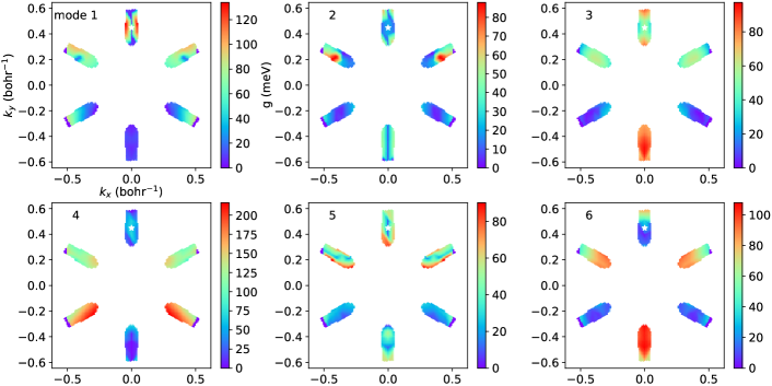
To investigate and explain the origin of this enhancement factor, we first observe that the EPCs are essentially the same for the strained and equilibrium case, as it can be observed by comparing Fig. 2 with an equivalent plot for the strained case (Fig. S1 of the Supporting Information). Therefore, strain does not change the nature or strength of the EPCs, but it affects the relative energy of the states in the valleys, effectively turning off some intervalley scattering channels by moving the corresponding final states out of reach. From our computed scattering times taken at the Fermi level, we determine that scattering decreases by a factor , as shown in Fig. 4, which is consistent with the approximate mode-by-mode contributions indicated in Fig. 2. The suppression of intervalley scattering is thus the major contribution to the improvement of the conductivity.
There are other contributions originating from the change of symmetry and electronic structure that must be taken into account. First, strain can affect the effective masses, although we find this effect to be negligible here (see Supporting Information C). Two other effects, however, do play a significant role, even if they happen to nearly compensate each other here. The first of those effects is the following: the conductivity becomes a sum of contributions from only two valleys instead of six, corresponding to a loss in density of states, and it is direction-dependent. In fact, performing the sum of Eq. (3) over the two remaining valleys at we get for the conductivity in the strained case:
| (6) |
The conductivity for an electric field in the high-velocity direction now is only twice the conductivity of the reference valley (), in contrast to of Eq. (5) for the equilibrium case. Therefore, if we were to ignore the six-fold enhancement of mobility from the suppression of the intervalley scattering discussed above and assume that the contributions from a single valley did not change (i.e., , ), we would actually obtain that the removal of four valleys would degrade conductivity significantly. Single-valley conductivities in high- and low-velocity directions are numerically ; so, the conductivity in the strained case would become a factor smaller in the high-velocity direction, down to a factor along the low-velocity direction.
However, this loss happens to be compensated by a second effect: an increase of the Fermi level within the two remaining valleys. Assuming as mentioned above that the charge density does not change under strain, the fact that only two valleys are now occupied instead of six implies that those valleys must contain three times as many carriers, which corresponds to an increase of the Fermi level with respect to the band edge. As the overall implications on the conductivity Eq. (4) are not straightforward, we study the effect of a rigid Fermi level shift on conductivity in the equilibrium and strained case. The results are reported as a function of carrier density in Fig. 5. Carrier density is the appropriate variable when comparing strained and equilibrium arsenene. Indeed, in an experimental measurement of transport properties as a function of strain, the carrier density would stay mostly constant, fixed by the gate. Note that even at the maximum doping of cm-2, no additional conduction-band minima need to be taken into account (band minima appear around K and for eigenenergies beyond the range considered in this work). We highlight some points of interest. The square and circle indicate conductivities for the systems at the carrier density studied in this work. To compare the conductivities at similar Fermi energy relative to the band edge, the density of equilibrium arsenene should be three times that of strained arsenene, corresponding to the triangle. The resulting conductivity is roughly twice larger. This also holds for strained arsenene at small enough densities, with a conductivity twice larger at cm-2 than at cm-2, although at densities above cm-2 the Fermi level would reach the four shifted valleys and the conductivity decreases. Nevertheless, staying in the doping regime of interest, the increase in Fermi level occurring in the strained case with respect to equilibrium due to the need to fill fewer valleys with the same charge can be associated with an improvement in conductivity by a factor approximately equal to two. Therefore, we conclude that the increase in Fermi level and associated doubling in conductivity compensates the loss of a factor associated to the reduced number of valleys (at fixed scattering), leaving the major role in the six-fold improvement of the conductivity to the suppression of intervalley scattering. Interestingly, we can also infer from Fig. 5 that there is an optimal density, around cm-2, that maximizes the enhancement of the transport properties for a strain. Finally, we also provide an estimation of the dependency of the conductivity enhancement as a function of strain in the Supporting Information B, assuming a linear relationship between the strain and the shift of the valleys. As can be expected, the strain-dependent enhancement is not monotonic: it increases slowly at small strain and saturates at high strain. Based on the shifts induced by strain and the computation of electron-phonon couplings in the equilibrium case, similar results are expected in antimonene and blue phosphorene (see Supporting Information).
In conclusion, we have put forward a general approach to enhance the mobility of 2D materials by engineering their valley structure. We have illustrated this approach in detail in the case of electron-doped arsenene, using a uniaxial strain field to modify the valley configuration and intervalley scattering. Indeed, a moderate and physically attainable strain induces a relative change in the energy of the six equivalent conduction valleys, shifting four of them out of reach for phonon-mediated scattering. The overall effect on the transport properties of arsenene results from a complex interplay of different mechanisms. Using accurate first-principles simulations of the electron-phonon interactions that take into account the reduced dimensionality and the field-effect doping of the system, we show that the main effect arises from the suppression of intervalley scattering, with a substantial six-fold enhancement of the electron mobility. Similar results can be expected also for other isoelectronic group-V buckled monolayers, such as antimonene and blue phosphorene, as well as for other multivalley 2D materials, suggesting valley-engineering as a general and viable way to design the mobility of 2D materials, with potential applications in next-generation electronics.
Acknowledgements.
We acknowledge useful discussions with Alberto Morpurgo. This work was supported by the NCCR MARVEL of the Swiss National Science Foundation. G.P. acknowledges also support from the EU Centre of Excellence MaX “Materials design at the Exascale” (grant no. 824143). D.C. from the ‘EPFL Fellows’ fellowship programme co-funded by Marie Sklodowska-Curie, Horizon 2020 grant agreement no. 665667, M.G. from the Swiss National Science Foundation (SNSF) through the Ambizione career program (grant no. 174056). Simulation time was awarded by CSCS on Piz Daint (production project s825) and by PRACE on Marconi at Cineca, Italy (project id. 2016163963).I Supporting Information
.1 Electron-phonon scattering in strained arsenene
Fig. S1 shows that the electron-phonon couplings for strained arsenene are very similar to the ones of equilibrium arsenene reported in the main text.
We also provide the phonon dispersion in equilibrium and strained arsenene in Fig S2.
.2 Strain-dependent conductivity enhancement
In Fig. S3, we show an estimation of the conductivity enhancement as a function of strain. We assume a linear relationship between strain and the energy shift of the valleys. We use the electron-phonon coupling matrix elements of arsenene strained by . This implies that we neglect the changes of electron-phonon due to strain. This approximation has marginal effects, as the conductivity at zero strain is well reproduced. We keep the doping carrier density constant and the Fermi level is recomputed for each strain. We see that the conductivity enhancement is not linear. It increases slowly at small strain, while the valleys are still below the Fermi level. Then we observe a steady increase of the enhancement as the valleys become less and less accessible for scattering. Finally, above , the enhancement saturates, as the shifted valleys are already out of reach.
.3 Variation with strain of the effective masses
Fig. S4 shows the modification of the effective masses induced by strain. The curvature decreases by in the high velocity direction and by in the low velocity direction. The effect would be squared in the conductivity, and thus induce a slight degradation of the transport properties. We are mainly interested in transport along the high velocity direction, for which we estimate a decrease of conductivity due to the change of effective masses. The decrease would be larger in the low velocity direction, but still negligible with respect to the other contributions discussed in the main text, which induce variations of or more.
.4 Antimonene
Fig. S5 shows the effect of strain on the bands of antimonene. The shift in energy due to strain is smaller but still significant and enough to make the shifted valleys out of reach for phonon-mediated processes. Fig. S6 shows the electron-phonon couplings in antimonene at equilibrium. The transport properties computed from these results are very similar to those of arsenene, with a room-temperature mobility of 62 cm2V-1s-1 for the same doping of cm-2. Thus, we can expect a slightly smaller but similar enhancement of mobility in strained antimonene.
.5 Blue Phosphorene
Fig. S7 shows the effect of strain on the bands of blue phosphorene. The shift in energy due to strain is significant ( eV). Fig. S8 shows the electron-phonon couplings in blue phosphorene at equilibrium. We observe a large intravalley coupling for the first mode, which would decrease the relative importance of the intervalley modes and thus the enhancement. The transport properties computed from those results are better than those of arsenene, with a room-temperature mobility of 150 cm2V-1s-1 for the same doping of cm-2. This is probably due to the more elongated nature of the valley mentioned in Fig. S7. Overall, with less enhancement but better performance at equilibrium, one can expect similar performances for strained blue phosphorene.
.6 Raman spectrum of Arsenene
In Table SI and Fig. S9, we give the frequencies of the Raman active modes and the Raman spectra for arsenene at equilibrium and strained in both and directions. The calculations are based on ab-initio, finite differences evaluations of the dielectric tensor derivatives. To compute the spectrum, we considered a back-scattering geometry in non-resonant conditionsSosso2011 ; Wang2016 , for which the differential cross section can be expressed as:
| (S1) |
where and are the frequencies of the scattered photons and of the -th phonon respectively, and the polarization vectors of the scattered and incident light, and the Raman tensor. In the case of unpolarized light averaged over the in-plane directions the Raman cross section can be obtained from the equivalence:
| (S2) |
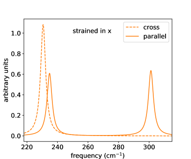
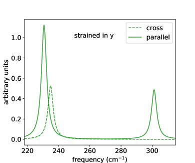
The spectra obtained under these conditions for the strained and unstrained cases are reported in Fig. S9. The magnitude of the shifts in frequency of the peaks should allow to follow the strain in the material. The order of the Ag and Bg modes in the strained case could be used to determine whether arsenene is strained in the (zig-zag) or (armchair) direction Mohiuddin2009 ; Huang2009 . Ag and Bg modes can be distinguished using polarized incident light along the strain direction and measuring the scattered light polarized in the parallel or perpendicular (cross) direction. The Raman cross section in the two cases is given by:
| (S3) |
and
| (S4) |
where indicates the strain direction. The spectra for the two strain directions and polarization combinations are reported in Fig. S10.
| Material | Frequency (cm-1) | Character |
| As equilibirum | 236.4 | Eg |
| As equilibrium | 304.9 | A1g |
| As 2% strain | 230.6 | Bg |
| As 2% strain | 234.8 | Ag |
| As 2% strain | 301.2 | Ag |
| As 2% strain | 230.5 | Ag |
| As 2% strain | 234.9 | Bg |
| As 2% strain | 301.2 | Ag |
References
- (1) Q. H. Wang, K. Kalantar-Zadeh, A. Kis, J. N. Coleman, and M. S. Strano, Electronics and optoelectronics of two-dimensional transition metal dichalcogenides, Nat. Nanotech. 7, 699 (2012).
- (2) G. Fiori, F. Bonaccorso, G. Iannaccone, T. Palacios, D. Neumaier, A. Seabaugh, S. K. Banerjee, and L. Colombo, Electronics based on two-dimensional materials, Nature Nanotechnology 9, 768 (2014).
- (3) M. Chhowalla, D. Jena, and H. Zhang, Two-dimensional semiconductors for transistors, Nature Reviews Materials 1, 16052 EP (2016).
- (4) H. Wang, X. Wang, F. Xia, L. Wang, H. Jiang, Q. Xia, M. L. Chin, M. Dubey, and S.-j. Han, Black Phosphorus Radio-Frequency Transistors, Nano Letters 14, 6424 (2014).
- (5) S. Das, R. Gulotty, A. V. Sumant, and A. Roelofs, All Two-Dimensional, Flexible, Transparent, and Thinnest Thin Film Transistor, Nano Letters 14, 2861 (2014).
- (6) D. Akinwande, N. Petrone, and J. Hone, Two-dimensional flexible nanoelectronics, Nature Communications 5, 5678 EP (2014).
- (7) J. J.-H. Chen, C. Jang, S. Xiao, M. Ishigami, and M. S. Fuhrer, Intrinsic and extrinsic performance limits of graphene devices on SiO2, Nature Nanotechnology 3, 206 (2008).
- (8) C. R. Dean, A. F. Young, I. Meric, C. Lee, L. Wang, S. Sorgenfrei, K. Watanabe, T. Taniguchi, P. Kim, K. L. Shepard, and J. Hone, Boron nitride substrates for high-quality graphene electronics., Nature nanotechnology 5, 722 (2010).
- (9) D. K. Efetov and P. Kim, Controlling Electron-Phonon Interactions in Graphene at Ultrahigh Carrier Densities, Physical Review Letters 105, 256805 (2010).
- (10) A. S. Mayorov, R. V. Gorbachev, S. V. Morozov, L. Britnell, R. Jalil, L. A. Ponomarenko, P. Blake, K. S. Novoselov, K. Watanabe, T. Taniguchi, and A. K. Geim, Micrometer-Scale Ballistic Transport in Encapsulated Graphene at Room Temperature, Nano Letters 11, 2396 (2011).
- (11) L. Wang, I. Meric, P. Y. Huang, Q. Gao, Y. Gao, H. Tran, T. Taniguchi, K. Watanabe, L. M. Campos, D. A. Muller, J. Guo, P. Kim, J. Hone, K. L. Shepard, and C. R. Dean, One-Dimensional Electrical Contact to a Two-Dimensional Material, Science 342, 614 (2013).
- (12) F. Schwierz, Graphene transistors, Nature Nanotechnology 5, 487 (2010).
- (13) A. N. Grigorenko, M. Polini, and K. S. Novoselov, Graphene plasmonics, Nature Photonics 6, 749 (2012).
- (14) P. Tassin, T. Koschny, and C. M. Soukoulis, Graphene for Terahertz Applications, Science 341, 620 (2013).
- (15) Y. Yoon, K. Ganapathi, and S. Salahuddin, How Good Can Monolayer MoS2 Transistors Be?, Nano Letters 11, 3768 (2011).
- (16) B. Radisavljevic, A. Radenovic, J. Brivio, V. Giacometti, and A. Kis, Single-layer MoS2 transistors, Nature Nanotechnology 6, 147 (2011).
- (17) A. Allain and A. Kis, Electron and Hole Mobilities in Single-Layer WSe2, ACS Nano 8, 7180 (2014).
- (18) S. Jo, N. Ubrig, H. Berger, A. B. Kuzmenko, and A. F. Morpurgo, Mono- and Bilayer WS2 Light-Emitting Transistors, Nano Letters 14, 2019 (2014).
- (19) T. Sohier, D. Campi, N. Marzari, and M. Gibertini, Mobility of 2D materials from first principles in an accurate and automated framework, Physical Review Materials 2, 114010 (2018).
- (20) R. Roldán, A. Castellanos-Gomez, E. Cappelluti, and F. Guinea, Strain engineering in semiconducting two-dimensional crystals, Journal of Physics: Condensed Matter 27, 313201 (2015).
- (21) T. M. Mohiuddin, A. Lombardo, R. R. Nair, A. Bonetti, G. Savini, R. Jalil, N. Bonini, D. M. Basko, C. Galiotis, N. Marzari, K. S. Novoselov, A. K. Geim, and A. C. Ferrari, Uniaxial strain in graphene by Raman spectroscopy: G peak splitting, Grüneisen parameters, and sample orientation, Physical Review B - Condensed Matter and Materials Physics 79, 205433 (2009).
- (22) P. San-Jose, A. Gutiérrez-Rubio, M. Sturla, and F. Guinea, Spontaneous strains and gap in graphene on boron nitride, Physical Review B - Condensed Matter and Materials Physics 90, 075428 (2014).
- (23) J. Jung, A. M. Dasilva, A. H. Macdonald, and S. Adam, Origin of band gaps in graphene on hexagonal boron nitride, Nature Communications 6, 6308 (2015).
- (24) D. R. Kripalani, A. A. Kistanov, Y. Cai, M. Xue, and K. Zhou, Strain engineering of antimonene by a first-principles study: Mechanical and electronic properties, Physical Review B 98, 085410 (2018).
- (25) A. Steinhoff, J.-H. Kim, F. Jahnke, M. Rösner, D. S. Kim, C. Lee, G. H. Han, M. S. Jeong, T. O. Wehling, and C. Gies, Efficient Excitonic Photoluminescence in Direct and Indirect Band Gap Monolayer MoS2, Nano Letters 15, 6841 (2015).
- (26) J. Lee, Z. Wang, H. Xie, K. F. Mak, and J. Shan, Valley magnetoelectricity in single-layer MoS2, Nature Materials 16, 887 (2017).
- (27) N. Ma, S. Zhang, and D. Liu, Mechanical control over valley magnetotransport in strained graphene, Physics Letters, Section A: General, Atomic and Solid State Physics 380, 1884 (2016).
- (28) T. Shen, A. V. Penumatcha, and J. Appenzeller, Strain Engineering for Transition Metal Dichalcogenides Based Field Effect Transistors, ACS Nano 10, 4712 (2016).
- (29) S. Zhang, Z. Yan, Y. Li, Z. Chen, and H. Zeng, Atomically Thin Arsenene and Antimonene: Semimetal–Semiconductor and Indirect–Direct Band-Gap Transitions, Angew. Chem. Int. Ed. 54, 3112 (2015).
- (30) J. Shah, W. Wang, H. M. Sohail, and R. I. G. Uhrberg, Experimental evidence of monolayer arsenene: An exotic two-dimensional semiconducting material, arXiv:1812.05978 (2018).
- (31) S. M. Beladi‐Mousavi, A. M. Pourrahimi, Z. Sofer, and M. Pumera, Atomically Thin 2D‐Arsenene by Liquid‐Phased Exfoliation: Toward Selective Vapor Sensing, Advanced Functional Materials 29, 1807004 (2019).
- (32) Y. Ge, W. Wan, W. Feng, D. Xiao, and Y. Yao, Effect of doping and strain modulations on electron transport in monolayer , Physical Review B 90, 035414 (2014).
- (33) Y. Sun, S. E. Thompson, and T. Nishida, Physics of strain effects in semiconductors and metal-oxide-semiconductor field-effect transistors, Journal of Applied Physics 101, 104503 (2007).
- (34) S. Takagi, T. Iisawa, T. Tezuka, T. Numata, S. Nakaharai, N. Hirashita, Y. Moriyama, K. Usuda, E. Toyoda, S. Dissanayake, M. Shichijo, R. Nakane, S. Sugahara, M. Takenaka, and N. Sugiyama, Carrier-Transport-Enhanced Channel CMOS for Improved Power Consumption and Performance, IEEE Transactions on Electron Devices 55, 21 (2008).
- (35) D. Yu, Y. Zhang, and F. Liu, First-principles study of electronic properties of biaxially strained silicon: Effects on charge carrier mobility, Phys. Rev. B 78, 245204 (2008).
- (36) M. Chu, Y. Sun, U. Aghoram, and S. E. Thompson, Strain: A Solution for Higher Carrier Mobility in Nanoscale MOSFETs, Annual Review of Materials Research 39, 203 (2009).
- (37) N. Xu, B. Ho, F. Andrieu, L. Smith, B. Nguyen, O. Weber, T. Poiroux, O. Faynot, and T. K. Liu, Carrier-Mobility Enhancement via Strain Engineering in Future Thin-Body MOSFETs, IEEE Electron Device Letters 33, 318 (2012).
- (38) T. Vogelsang and K. R. Hofmann, Electron mobilities and high-field drift velocities in strained silicon on silicon-germanium substrates, IEEE Transactions on Electron Devices 39, 2641 (1992).
- (39) T. Vogelsang and K. R. Hofmann, Electron transport in strained Si layers on Si1-xGex substrates, Applied Physics Letters 63, 186 (1993).
- (40) S. Takagi, J. L. Hoyt, J. J. Welser, and J. F. Gibbons, Comparative study of phonon-limited mobility of two-dimensional electrons in strained and unstrained Si metal-oxide-semiconductor field-effect transistors, Journal of Applied Physics 80, 1567 (1996).
- (41) A. Rahman, M. S. Lundstrom, and A. W. Ghosh, Generalized effective-mass approach for n-type metal-oxide-semiconductor field-effect transistors on arbitrarily oriented wafers, Journal of Applied Physics 97, 053702 (2005).
- (42) K. Uchida, T. Krishnamohan, K. C. Saraswat, and Y. Nishi, in Technical Digest - International Electron Devices Meeting, IEDM, Vol. 2005 (2005) pp. 129–132, ISBN 078039268X
- (43) S. Yu, H. Zhu, K. Eshun, C. Shi, M. Zeng, and Q. Li, Strain-engineering the anisotropic electrical conductance in ReS2 monolayer, Applied Physics Letters 108, 191901 (2016).
- (44) Y. Aierken, D. Cakır, and F. M. Peeters, Strain enhancement of acoustic phonon limited mobility in monolayer TiS3, Phys. Chem. Chem. Phys. 18, 14434 (2016).
- (45) Y. Shao, F. Zhang, X. Shi, and H. Pan, N-Functionalized MXenes: ultrahigh carrier mobility and multifunctional properties, Phys. Chem. Chem. Phys. 19, 28710 (2017).
- (46) Y. Xu, Z. Ning, H. Zhang, G. Ni, H. Shao, B. Peng, X. Zhang, X. He, Y. Zhu, and H. Zhu, Anisotropic ultrahigh hole mobility in two-dimensional penta-SiC2 by strain-engineering: electronic structure and chemical bonding analysis, RSC Adv. 7, 45705 (2017).
- (47) H. V. Phuc, N. N. Hieu, B. D. Hoi, N. V. Hieu, T. V. Thu, N. M. Hung, V. V. Ilyasov, N. A. Poklonski, and C. V. Nguyen, Tuning the Electronic Properties, Effective Mass and Carrier Mobility of MoS2 Monolayer by Strain Engineering: First-Principle Calculations, Journal of Electronic Materials 47, 730 (2018).
- (48) R. Fang, X. Cui, M. A. Khan, C. Stampfl, S. P. Ringer, and R. Zheng, Strain-Engineered Ultrahigh Mobility in Phosphorene for Terahertz Transistors, Advanced Electronic Materials 0, 1800797.
- (49) L. Liu, X. Wu, X. Liu, and P. K. Chu, Strain-induced band structure and mobility modulation in graphitic blue phosphorus, Applied Surface Science 356, 626 (2015).
- (50) A. Priydarshi, Y. S. Chauhan, S. Bhowmick, and A. Agarwal, Strain-tunable charge carrier mobility of atomically thin phosphorus allotropes, Phys. Rev. B 97, 115434 (2018).
- (51) Z. Xie, F. Sun, R. Yao, Y. Zhang, Y. Zhang, Z. Zhang, J. Fan, L. Ni, and L. Duan, Tuning electronic properties of InSe/arsenene heterostructure by external electric field and uniaxial strain, Applied Surface Science 475, 839 (2019).
- (52) S. Takagi, A. Toriumi, M. Iwase, and H. Tango, On the universality of inversion layer mobility in Si MOSFET’s: Part I-effects of substrate impurity concentration, IEEE Transactions on Electron Devices 41, 2357 (1994).
- (53) F. Giustino, Electron-phonon interactions from first principles, Reviews of Modern Physics 89, 015003 (2017).
- (54) J. M. Ziman, Electrons and phonons: the theory of transport phenomena in solids (Clarendon, Oxford, 1960).
- (55) G. Grimvall, The electron-phonon interaction in metals (North-Holland, Amsterdam, 1981).
- (56) S. Baroni, S. De Gironcoli, A. Dal Corso, and P. Giannozzi, Phonons and related crystal properties from density-functional perturbation theory, Reviews of Modern Physics 73, 515 (2001).
- (57) T. Sohier, M. Calandra, and F. Mauri, Density functional perturbation theory for gated two-dimensional heterostructures: Theoretical developments and application to flexural phonons in graphene, Physical Review B 96, 075448 (2017).
- (58) C.-H. Park, N. Bonini, T. Sohier, G. Samsonidze, B. Kozinsky, M. Calandra, F. Mauri, and N. Marzari, Electron-Phonon Interactions and the Intrinsic Electrical Resistivity of Graphene., Nano letters 14, 1113 (2014).
- (59) T. Sohier, M. Calandra, C.-H. C.-H. Park, N. Bonini, N. Marzari, and F. Mauri, Phonon-limited resistivity of graphene by first-principles calculations: Electron-phonon interactions, strain-induced gauge field, and Boltzmann equation, Physical Review B 90, 125414 (2014).
- (60) J. Ji, X. Song, J. Liu, Z. Yan, C. Huo, S. Zhang, M. Su, L. Liao, W. Wang, Z. Ni, Y. Hao, and H. Zeng, Two-dimensional antimonene single crystals grown by van der Waals epitaxy, Nature Communications 7, 13352 (2016).
- (61) W. Zhang, H. Enriquez, Y. Tong, A. Bendounan, A. Kara, A. P. Seitsonen, A. J. Mayne, G. Dujardin, and H. Oughaddou, Epitaxial Synthesis of Blue Phosphorene, Small 14, 1804066 (2018).
- (62) N. Mounet, M. Gibertini, P. Schwaller, D. Campi, A. Merkys, A. Marrazzo, T. Sohier, I. E. Castelli, A. Cepellotti, G. Pizzi, and N. Marzari, Two-dimensional materials from high-throughput computational exfoliation of experimentally known compounds, Nature Nanotechnology 13, 246 (2018).
- (63) G. Pizzi, M. Gibertini, E. Dib, N. Marzari, G. Iannaccone, and G. Fiori, Performance of arsenene and antimonene double-gate MOSFETs from first principles, Nature Communications 7, 12585 (2016).
- (64) J. Nye, Physical properties of crystals: Their representation by tensor and matrices (Oxford University Press, 1957).
- (65) According to Ref. \rev@citealpnumPizzi2016a the deformation potential of the conduction valleys is positive in the longitudinal direction and negative in the transverse direction, so that with a strain along the direction two valleys (the ones with longitudinal direction along ) are pushed down and the other four are pushed up, while the opposite is true (two up and four down) for strain along the direction.
- (66) In practice, depending on the experimental setup, such an uniaxial stretch might be accompanied by a compression in the perpendicular direction. This is not included in our simulations, but we checked that the effects of a full relaxation in the perpendicular direction are minimal.
- (67) M. Huang, H. Yan, C. Chen, D. Song, T. F. Heinz, and J. Hone, Phonon softening and crystallographic orientation of strained graphene studied by Raman spectroscopy, Proceedings of the National Academy of Sciences 106, 7304 (2009).
- (68) G. Prandini, A. Marrazzo, I. E. Castelli, N. Mounet, and N. Marzari, Precision and efficiency in solid-state pseudopotential calculations, npj Computational Materials 4, 72 (2018).
- (69) G. C. Sosso, S. Caravati, R. Mazzarello, and M. Bernasconi, Raman spectra of cubic and amorphous Ge2Sb2Te5 from first principles, Phys. Rev. B 83, 134201 (2011).
- (70) R. Wang, D. Campi, M. Bernasconi, J. Momand, B. J. Kooi, M. A. Verheijen, M. Wuttig, and R. Calarco, Ordered Peierls distortion prevented at growth onset of GeTe ultra-thin films, Scientific Reports 6, 32895 (2016).