Deterministic field-free skyrmion nucleation at a nano-engineered injector device
Abstract
Magnetic skyrmions are topological solitons that exhibit an increased stability against annihilation Fert et al. (2013); Büttner et al. (2018), and can be displaced with low current densities Schulz et al. (2012), making them a promising candidate as an information carrier Fert et al. (2013). In order to demonstrate a viable skyrmion-based memory device, it is necessary to reliably and reproducibly nucleate, displace, detect, and delete the magnetic skyrmions. While the skyrmion displacement Jiang et al. (2017); Litzius et al. (2017); Woo et al. (2018a, 2016) and detection Zeissler et al. (2018); Maccariello et al. (2018) have both been investigated in detail, much less attention has been dedicated to the study of the sub-ns dynamics of the skyrmion nucleation process. Only limited studies on the statics Büttner et al. (2017); Jiang et al. (2015) and above-ns dynamics Woo et al. (2018b) have been performed, leaving still many open questions on the dynamics of the nucleation process. Furthermore, the vast majority of the presently existing studies focus on the nucleation from random natural pinning sites Büttner et al. (2017); Woo et al. (2018b), or from patterned constrictions in the magnetic material itself Büttner et al. (2017); Jiang et al. (2015), which limit the functionality of the skyrmion-based device. Those limitations can be overcome by the fabrication of a dedicated injector device on top of the magnetic material Hrabec et al. (2017). In this study, we investigate the nucleation of magnetic skyrmions from a dedicated nano-engineered injector, demonstrating the reliable magnetic skyrmion nucleation at the remnant state. The sub-ns dynamics of the skyrmion nucleation process were also investigated, allowing us to shine light on the physical processes driving the nucleation.
Magnetic skyrmions are topological quasi-particles that can be stabilized in perpendicularly magnetized (PMA) materials exhibiting an anti-symmetric exchange interaction (Dzyaloshinskii-Moriya - DM - interaction). The DM interaction arises from the breaking of the inversion symmetry in the magnetic material Dzyaloshinskii (1958); Moriya (1960). For multilayered PMA thin film systems where the inversion symmetry is broken at the interface between the different layers that compose the superlattice stack, the resulting interfacial DM interaction leads to the stabilization of Néel-type magnetic domain walls and skyrmions Finizio et al. (2018a); Boulle et al. (2016); Zeissler et al. (2018). Examples of multilayer stacks where room-temperature Néel-type magnetic skyrmions can be stabilized include Pt/Co/Ir Moreau-Luchaire et al. (2016), Pt/Co/MgO Boulle et al. (2016), and Pt/CoFeB/MgO Litzius et al. (2017).
As a consequence of their non-trivial topology, magnetic skyrmions exhibit an increased stability against annihilation and pinning at defects Fert et al. (2013); Büttner et al. (2018), a topological contribution to the Hall resistivity Nagaosa and Tokura (2013); Zeissler et al. (2018), and they can be displaced with low current densities down to 106-107 Am-2 for single-crystalline materials exhibiting bulk DM interaction at cryogenic temperatures Fert et al. (2013); Schulz et al. (2012). The combination of these properties makes magnetic skyrmions particularly interesting both for fundamental studies and for applications in novel non-volatile magnetic memory concepts such as the skyrmion racetrack memory Fert et al. (2013).
In order to fabricate a viable skyrmion-based memory, the controllable and reproducible nucleation, motion, detection, and deletion of the magnetic skyrmions needs to be demonstrated. Skyrmion motion has been object of profound attention in the last years, leading to not only the demonstration of a reliable current-driven motion Jiang et al. (2017); Litzius et al. (2017); Woo et al. (2018a, 2016), but also to the study of the dynamics of the spin-orbit torque (SOT)-induced skyrmion motion Litzius et al. (2017). Due to the influence of the skyrmion topology on its transport properties (giving rise e.g. to the topological Hall effect Nagaosa and Tokura (2013)), also the electrical detection of magnetic skyrmions has been thoroughly investigated, ranging from the investigation of the topological Hall effect in skyrmion crystals in materials exhibiting bulk DM interaction Nagaosa and Tokura (2013) to the detection of isolated magnetic skyrmions in multilayer stacks exhibiting interfacial DM interaction Zeissler et al. (2018); Maccariello et al. (2018).
However, only a limited experimental attention has been dedicated to the controlled nucleation of such magnetic quasi-particles. These studies mostly focus on the nucleation of magnetic skyrmions arising from natural or artificially fabricated defects in the magnetic material Büttner et al. (2017); Woo et al. (2018b), or from constrictions patterned directly into the magnetic material Büttner et al. (2017); Jiang et al. (2015). However, the properties of a natural defect site cannot be directly controlled, as different defect sites are not reproducibly equal both within the same and between different samples, making them unsuitable for the reliable and reproducible skyrmion nucleation that would be required in a device. Furthermore, due to the difficulty in determining the exact properties of the material in the defect site (e.g. the local values of the saturation magnetization or of the PMA), the interpretation of the processes occurring during the nucleation has to rely on a-priori assumptions on the properties of the defect site Woo et al. (2018b); Büttner et al. (2017), or involve challenging investigations of the material Hanneken et al. (2016). In the case that the skyrmion nucleation is achieved through a patterned constriction in the magnetic material Büttner et al. (2017); Jiang et al. (2015), the fabrication of the constriction itself requires a precise patterning, unnecessarily constraining its geometry. A constrained device geometry leads to a limited functionality of the magnetic device, complicating the design of a skyrmion-based memory employing such nucleators.
The fabrication of a constriction in the magnetic material leads to a non-uniform local distribution of the current density, which is then employed for the spatially-defined nucleation of the magnetic skyrmions Büttner et al. (2017); Jiang et al. (2015). However, one can also employ a patterned contact structure for achieving a non-uniform distribution of the current density, as proposed in the work of A. Hrabec et al. Hrabec et al. (2017). This design is a viable alternative for the electrical skyrmion nucleation, as a dedicated injector requires neither the direct patterning of the magnetic material nor to rely on natural or artificial defect sites. However, no detailed experimental investigations on the processes (and on their dynamics) that lead to the nucleation of a magnetic skyrmion from a dedicated injector device have been carried out as of now, leaving open questions on the physical mechanisms driving the nucleation.
Moreover, all of the currently available studies on the current-induced skyrmion nucleation require a permanently applied out-of-plane magnetic field for the stabilization of the magnetic skyrmions. The magnetic fields range in magnitude from sub-10 mT Büttner et al. (2017); Jiang et al. (2015); Hrabec et al. (2017) to above 100 mT Woo et al. (2018b). The requirement of a permanently applied magnetic field is strongly detrimental for an application of magnetic skyrmions as an information carrier. A completely field-free stability of the nucleated skyrmions would instead be strongly desirable, as this would avoid the requirement of integrating permanent out-of-plane magnetic fields in the skyrmion-based device.
With the experiments presented in this work, we have overcome the issues discussed above by demonstrating the controlled skyrmion nucleation from a nano-engineered injector device. The injector was tailored to achieve a high current density at its tip, designating the region where the magnetic skyrmion is nucleated. The injector was fabricated on top of a Ta(3.2 nm)/Pt(2.6 nm)/[Co68B32(0.8 nm)/Ir(0.4 nm)/Pt(0.6nm)]×3/Pt(2.1 nm) PMA stack. This stack, from now on referred to as Pt/Co68B32/Ir, was tailored to allow for the stabilization of magnetic skyrmions at the remnant state, therefore removing the requirement to carry out the experiments in presence of a permanently applied magnetic field. Additionally, the patterning of a nanostructured injector device on top of the Pt/Co68B32/Ir stack allows for the deterministic current-induced nucleation of magnetic skyrmions without the necessity to rely on random natural defects of the material, or on constrictions patterned directly into the material. Finally, thanks to the use of time-resolved scanning transmission X-ray microscopy (STXM), the sub-ns dynamical processes leading to the current-induced skyrmion nucleation (and magnetic field-induced deletion) could be unraveled.
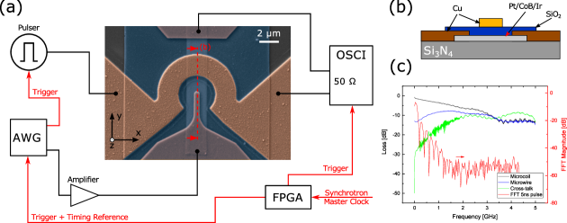
For the skyrmion nucleation and deletion experiments reported here, we fabricated 500 nm wide Cu skyrmion injector structures on top of a Pt/Co68B32/Ir microwire (see Figs. 1(a-b) and the Methods section). Thanks to the use of Cu for the fabrication of the electrical contacts, the magnetic configuration of the Pt/Co68B32/Ir microwire could be investigated also in the regions covered by the Cu contacts (see the Methods section). The skyrmion nucleation (starting from a uniformly magnetized state) is achieved by the injection of short current pulses from the Cu contact into the magnetic microwire. In order to reset the magnetic configuration back to a uniformly magnetized state within a ns timescale, a necessary condition to be able to perform time-resolved pump-probe experiments, an -shaped Cu microcoil was fabricated on top of the microwire. This allows for the generation of ns-wide out-of-plane magnetic field pulses that can be employed to magnetically saturate the region around the injector. Further details about the sample fabrication are provided in the Methods section. Note that the microwire and the microcoil are electrically insulated through the use of a 200 nm thick SiO2 insulation layer, and that the geometry of the samples was optimized to minimize reflections of the injected current pulses, and to minimize the cross-talk between the microcoil and the microwire (see the Methods section and Fig. 1(c) for more details).
The Pt/Co68B32/Ir multilayer stacks employed here stabilize Néel-type skyrmions at the remnant state (see Ref. Finizio et al. (2018a) for a proof that Néel-type domain walls are stabilized in this PMA stack). The zero-field skyrmion stability provides a strong motivation to use Pt/Co68B32/Ir stacks with respect to other common multilayer stacks that require the presence of an external out-of-plane magnetic field for the skyrmion stability Moreau-Luchaire et al. (2016); Büttner et al. (2015); Zeissler et al. (2017, 2018); Woo et al. (2018a, b); Litzius et al. (2017); Jiang et al. (2017); Büttner et al. (2017); Jiang et al. (2015); Hrabec et al. (2017). Because of this, we could perform the nucleation experiments at the remnant state, where the influence of external static magnetic fields on the nucleation and deletion processes can be safely ignored. This allows for an easier interpretation of the physical processes causing their nucleation and deletion, and removing the requirement to integrate a permanently-applied magnetic field with the skyrmion-based device.
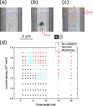
The skyrmion nucleation experiments were performed by STXM imaging both in the quasi-static and pump-probe regimes, using the X-ray magnetic circular dichroism (XMCD) effect Schütz et al. (1987) as a means to obtain the magnetic contrast (see the Methods section for additional details about the technique). A first verification of the conditions necessary for the skyrmion nucleation at the nanostructured injector contact was performed by quasi-static STXM imaging. Here, the magnetic configuration after the injection of a single current pulse of variable widths and amplitudes (the current densities shown in this work were calculated in the section of the microwire exhibiting a uniform current density - see the supplementary information and the Methods section for additional details) was investigated. Prior to the injection of each pulse, the microwire was initialized in a uniformly magnetized state by injecting a 4 ns wide current pulse across the microcoil (at a peak current of 350 mA, resulting in a peak out-of-plane magnetic field of 50 mT in the region surrounding the injector - see the Methods section and the supplementary information for additional details). An example of the quasi-static XMCD-STXM imaging experiments carried out in this part of our work is shown in Fig. 2(a-c), also depicting the nucleation and deletion protocol employed for the time-resolved experiments presented in the sections below.
As summarized in Fig. 2(d), we observed three different scenarios depending on the width and amplitude of the injected current pulse (all of the images employed to obtain the results shown in Fig. 2(d) are shown in the supplementary information). For low current densities (black squares in Fig. 2(d)), the uniformly magnetized state remained unchanged upon the injection of the current pulse. For high current densities (red circles in Fig. 2(d)), a multidomain state was nucleated. Between these two cases, a window of pulse widths and amplitudes leading to the reproducible nucleation of an isolated magnetic skyrmion was observed (light blue diamonds in Fig. 2(d)). A monotonic decrease of the threshold current density for both the nucleation of an isolated skyrmion and for the stochastic nucleation of a multi-domain state with the width of the current pulse can also be noticed in Fig. 2(d). It is also noteworthy that for the pulse widths and amplitudes considered here it was possible to nucleate a magnetic skyrmion with a pulse energy down to about 500 pJ, which is comparable to the energy required to write a bit in commercial NOR flash memories Wang et al. (2013). Further optimizations in the energy efficiency of the skyrmion nucleator presented here could therefore lead to a better energy performance than NOR flash memories, proving that the encoding of digital bits as magnetic skyrmions can be a competitive alternative.
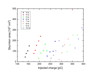
From the images where the nucleation of an isolated skyrmion was observed in Fig. 2(d), we extracted the area of the nucleated magnetic skyrmion as a function of the injected electrical charge. These results are shown in Fig. 3, where it is possible to observe that the area of the magnetic skyrmion exhibits a roughly linear dependence on the injected charge for a given pulse width, following a similar behavior observed for the partial SOT-induced switching of Pt/Co/AlOx nanodots Baumgartner et al. (2017), hinting that the SOTs are one of the driving mechanisms behind the skyrmion nucleation process. For longer pulses, the amount of charge required for the nucleation of a magnetic skyrmion with a similar area is higher than for shorter pulses with higher current densities. This behavior, along with the observation that the minimum nucleation current density decreases with an increasing pulse width, indicates that part of the energy of the pulse is spent in the heating of the material. The results are in agreement with the currently employed models for SOT-assisted magnetization switching Garello et al. (2014); Büttner et al. (2017), where a reduction in the switching current density with an increase of the temperature was observed Jinnai et al. (2018). A minimum skyrmion size with an area of 2.5 104 nm2, corresponding to a diameter of about 50 nm, was observed from the results presented in Fig. 3. This minimum skyrmion size is compatible with calculations of the domain periodicity at the remnant state in similar PMA multilayer stacks optimized for a high interfacial DM interaction Moreau-Luchaire et al. (2016).
After investigating the quasi-static skyrmion nucleation (and deletion) processes, we turned our attention to the time-resolved imaging of the dynamical processes behind the current-induced skyrmion nucleation and the magnetic field-induced skyrmion deletion. These experiments were performed by time-resolved STXM imaging using a 5 ns wide nucleation pulse with a current density of Am-2, and a 350 mA, 4 ns wide, deletion pulse. The results of one such time-resolved investigation are depicted in Fig. 4, where both the current-induced nucleation (Fig. 4(a)) and the magnetic field-induced deletion (Fig. 4(b)) are shown (videos of the time-resolved images can be found in the supplementary information). Figs. 4(c-d) depict respectively the time-resolved variation of the skyrmion area during the nucleation and deletion. Due to the requirements of the pump-probe technique, the current-induced nucleation and magnetic field-induced annihilation processes were repeated about 1010 times at a repetition frequency of 500 kHz, demonstrating that the nucleation and deletion processes are, within the limitations of the pump-probe technique, both reproducible and deterministic.
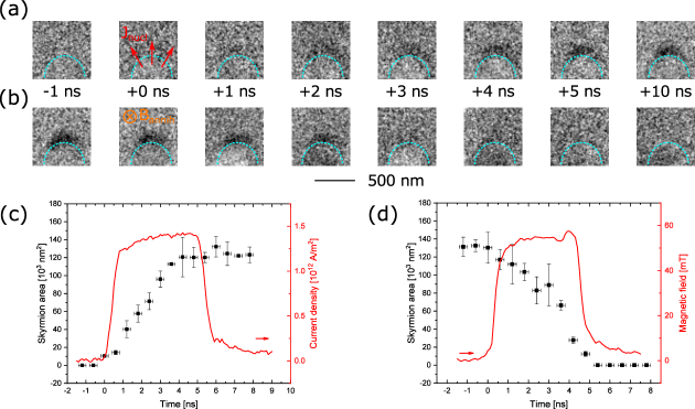
Thanks to the possibility of precisely determining the time position of the zero delay between pump and probe, the time-resolved variation of the skyrmion area can be overlaid and compared with the current/magnetic field excitation (see the Methods section for additional details). For both nucleation and deletion, it can be immediately observed from Figs. 4(c-d) that they do not exhibit a detectable incubation time within the 200 ps time step employed here and therefore start synchronously with the onset of the current/magnetic field pulse. The absence of an incubation time for the nucleation process provides, after the quasi-static behavior shown in Fig. 3, another indication that the nucleation is driven by SOT-induced switching of the magnetization, which instantaneously responds to the excitation Baumgartner et al. (2017).
Another observation that can be made from the time-resolved variation of the skyrmion area shown in Figs. 4(c-d) is that, for both the nucleation and deletion processes, the area of the magnetic skyrmion varies roughly linearly with the duration of the current/magnetic field pulse. This behavior is in agreement with the quasi-static experiments shown in Fig. 3, and additionally with time-resolved observations on the partial switching of Pt/Co/AlOx nanodots Baumgartner et al. (2017), providing yet another indication that SOTs drive the current-induced skyrmion nucleation.
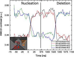
We also investigated the influence of the direction of the electrical current employed for the nucleation of the magnetic skyrmions. Here, we performed pump-probe imaging experiments of both the nucleation and deletion processes with a 2 ns probing time step as a function of the direction of both the nucleating and deleting pulses. The time-resolved change of the magnetic contrast in the region surrounding the injector structure during the nucleation and deletion processes was measured. Those results are shown in Fig. 5. The sign convention for the direction of the nucleation current and deletion magnetic field is shown in the inset of the figure, while the area where the time-resolved change in the magnetic contrast was measured is marked by ROI in the same inset. From the time traces shown in Fig. 5, it is possible to observe that a magnetic skyrmion can be nucleated for all four possible combinations of the directions of the nucleating current and deleting magnetic field. Moreover, the dynamics of the nucleation and deletion processes occur on the same timescales in all four combinations, indicating that the nucleation process occurs independently from the direction of the current flowing in the injector.
In the absence of static external magnetic fields, the four possible combinations of the directions of the nucleation current and deletion field are symmetric. The magnitude of the torque generated by the SOT effect will therefore be equal for all four possible combinations Baumgartner et al. (2017). If the injected spin current is sufficiently high, a switching of the magnetization will be observed Garello et al. (2014); Baumgartner et al. (2017); Büttner et al. (2017), independently of the direction of the spin current. The sign of the torque will be affected by the orientation of the electrical current, but it will nonetheless lead to a switching of the magnetization Baumgartner et al. (2017), in agreement with the results presented in Fig. 5.
Consequently, the results shown above allow us to conclude that the current-induced skyrmion nucleation process is driven by the SOT-induced switching of the magnetization in the area at the tip of the nano-engineered injector structure. It is however necessary to consider that the injection of the 5 ns-wide pulse considered here will lead, due to Ohmic losses, to the heating of the Pt/Co68B32/Ir microwire (see the supplementary information for a determination of the sample temperature from the time-resolved STXM images). The heating assists in the reduction of the critical current densities required to achieve a SOT-induced switching Jinnai et al. (2018). This indicates that the switching process is driven, for these pulse widths, by the synergy between the SOTs and the heating caused by the injected pulse.
As shown in Figs. 2 and 4 and in the figures and videos provided in the supplementary information, the nucleation of the magnetic skyrmion takes place at the tip of the injector structure. Nucleations outside of this region occur only for the pulses with current densities much higher than the single skyrmion nucleation threshold (see Fig. 2(d) and the images in the supplementary information). This can be explained by considering the geometry of the injector, and by the distribution of the current density during the injection of a current pulse (see the supplementary information for a finite-element simulation of the current density in the microwire). In particular, it can be observed that the magnitude of the current density at the tip of the injector is of about a factor 3 larger (in a circular region of about 150 nm in diameter) than the current density in the uniform section of the Pt/Co68B32/Ir microwire. The injector geometry presented here provides thus a localized "hot spot" with a higher current density that locally fulfills the requirements for the SOT-induced switching of the magnetization. On a first glance, this appears to be a similar concept to the SOT-induced nucleation of magnetic skyrmions at natural defects Woo et al. (2018b); Büttner et al. (2017) or, especially, at constrictions patterned directly on the magnetic material, which rely on a localized non-uniformity in the current distribution to facilitate the skyrmion nucleation Büttner et al. (2017); Jiang et al. (2015). However, while some similarities can be observed, our approach exhibits the advantage that the skyrmion nucleation does not rely on any natural (or artificial) defects and constrictions on the magnetic material, but on the patterning of an injector structure on top of the magnetic material. This avoids the necessity for the fabrication of controlled pinning sites on the magnetic material and, with the proposed design, the skyrmion injector structure can be fabricated directly on top of a skyrmion racetrack, where the nucleated skyrmions can then be displaced by a current pulse injected across the microwire (whilst maintaining the injector structure electrically floating). This design provides a simple method for nucleating the magnetic skyrmions, while allowing for the engineering of the functionality of the material by tailoring the design of the electrical contacts to the required process (e.g. displacement of the magnetic skyrmions in a racetrack memory element). Furthermore, the zero-field skyrmion stability provides a framework where magnetic skyrmions can be manipulated, allowing for the possibility to fabricate skyrmion-based devices free of any external permanent magnets.
In conclusion, we have shown that the fabrication of a nano-engineered injector structure on top of a Pt/Co68B32/Ir superlattice allows for the deterministic nucleation of isolated magnetic skyrmions at the remnant state by the injection of ns-wide current pulses. Quasi-static and time-resolved STXM imaging of the skyrmion nucleation process allowed us to observe that the process is driven by the SOT-induced local switching of the magnetization, and quasi-static STXM investigations of the properties of the switching pulses (width and current density) allowed us to conclude that the heating of the microwire also plays an important role in the switching process by reducing the threshold current density for longer pulses. The combination of the flexibility of the geometry of the magnetic material given by the use of an injector structure for the skyrmion nucleation with the zero field stability of the magnetic skyrmions in the Pt/Co68B32/Ir superlattice stack offers a leap forward towards the device applicability of magnetic skyrmions. In particular, our approach permits the generation of a skyrmion "where and when we want it", and will provide an easy framework where to investigate the skyrmion properties in absence of external fields.
I Methods
I.1 Sample fabrication and characterization
The microstructured wires were fabricated to a width of 2 m by electron beam lithography followed by liftoff out of a Ta(3.2 nm)/Pt(2.6 nm)/[Co68B32(0.8 nm)/Ir(0.4 nm)/Pt(0.6nm)]×3/Pt(2.1 nm) multilayer stack. The Pt/Co68B32/Ir stacks were deposited by magnetron sputtering at a rate of approximately 1 Ås-1 using an Ar plasma at a pressure of 3.2 mbar (base pressure of the deposition chamber in the low 10-8 mbar range). More details on the deposition of a similar multilayer stack can be found in Ref. Zeissler et al. (2017). For the lithographical fabrication, a bilayer of methyl-methacrylate (MMA) and of poly(methyl-methacrylate) (PMMA) resist was spincoated on top of 200 nm thick x-ray transparent Si3N4 membranes on 200 m thick high resistivity Si frames. The MMA/PMMA bilayer was exposed by electron beam lithography using a 100 kV Vistec EBPG 5000Plus electron beam writer with a writing dose of 1600 C cm-2. The exposed resist was developed by immersion for 90 s in a solution of methyl-isobutyl-ketone and isopropyl alcohol 1:3 in volume, followed by immersion in pure isopropyl alcohol for 60 s. After the deposition of the magnetic material, the unexposed resist, along with the magnetic film on top, was removed by immersion in pure acetone.
The microwires were contacted by 200 nm thick Cu electrodes fabricated by electron-beam lithography followed by liftoff. The Cu was deposited by thermal evaporation using a Balzers BAE250 thermal evaporator. One of the electrodes was fabricated in a rounded geometry with a 250 nm radius of curvature, designed to obtain a diverging current flow. To generate the magnetic field pulses employed for the deletion of the magnetic skyrmion, an -shaped, 400 nm thick, Cu microcoil was fabricated on top of the microwire once again by electron-beam lithography followed by a lift-off process. The microwire and the microcoil were electrically insulated through a 200 nm thick SiO2 layer deposited between the two layers by electron beam evaporation (using a Univex 450 electron beam evaporator). For all the layers, injector, insulator, and microcoil, the same process employed for the patterning of the magnetic material was utilized. Cu was chosen as electrode material as this guarantees a high x-ray transmittivity at the Co L3 edge, allowing for the investigation of the magnetic configuration of the sample also below the electrodes.
The quality of the samples fabricated according to the protocol described above was verified by scanning electron microscopy imaging (see Fig. 1(a)). Their electrical properties (in particular, the impedance matching of both the Pt/Co68B32/Ir microwire and the microcoil, and the cross-talk between the two) were verified by time-domain reflectometry measurements using an Agilent Infiniium DCA-J 86100C sampling oscilloscope. With this technique, the S21 parameters of the microwire, microcoil, and the cross-talk between them was determined. The results of this characterization are shown in Fig. 1(c). The electrical resistance of the samples, employed for monitoring the quality of the sample during the quasi-static and time-resolved STXM investigations, was measured using a Keithley 2400 source meter, employing a probing current of 10 A.
The magnetic properties of the Pt/Co68B32/Ir multilayer stacks were characterized by magnetometry measurements using a superconducting quantum interference device (SQUID). From these measurements, the temperature dependence of the saturation magnetization, employed to determine the time-resolved variation of the temperature close to the injector structure, could be determined.
I.2 Skyrmion nucleation and deletion protocol
The skyrmions were nucleated by injecting a current pulse across the injector structure. For the quasi-static investigations, the width and amplitude of the current pulse were varied from 1 to 20 ns and from to Am-2 respectively. For the time-resolved investigations, 5 ns wide current pulses with a peak current density of Am-2 were employed. The current pulses were generated using a Tektronix AWG 7122C 10 GSa s-1 arbitrary waveform generator (AWG) combined with a MiniCircuits ZPUL-30P non-inverting pulse amplifier. For the generation of the magnetic fields employed for the skyrmion deletion, 4 ns wide current pulses with a peak current of 350 mA were injected across the microcoil structure. A temporal gap of about 1 s between the current and magnetic field pulses was employed. The magnetic field pulses were generated using an Avtech AVM-4-C 20 V pulse generator, which was triggered by a synchronization signal generated with the second channel of the AWG. Both the nucleation and deletion pulses were monitored using a Keysight DSO-S 404A 20 GSa s-1real time oscilloscope. The oscilloscope was terminated with a 50 impedance, allowing for the measurement of the current flowing across the microwire and the microcoil. The electrical connections to the sample are shown in Fig. 1(a).
I.3 STXM imaging
The quasi-static and time-resolved STXM imaging of the skyrmion nucleation and deletion processes was performed using the STXM installed at the PolLux (X07DA) endstation of the Swiss Light Source Raabe et al. (2008). With STXM imaging, circularly-polarized monochromatic x-rays generated by the synchrotron light source (tuned to the Co L3 absorption edge) are focused on the sample using diffractive optics (Fresnel zone plate). The x-rays transmitted through the sample are recorded using an avalanche photodiode (APD) as photon detector. To form an image, the sample is raster scanned with a piezoelectric stage. For the experiments presented here, a Fresnel zone plate with a 25 nm outermost zone width was employed. The width of the entrance and exit slits to the beamline monochromator was selected to achieve an x-ray beam spot on the order of 25-30 nm, defining the spatial resolution of the images presented in this work.
The time-resolved images were acquired in the pump-probe regime illuminating the sample with circularly-polarized x-rays with negative helicity. Thanks to the use of a broadband APD, combined with a dedicated field-programmable gate array (FPGA) setup (which handles also the synchronization between the x-ray pulses and the electronics that excite the sample - see Fig. 1(a)), the entire filling pattern of the synchrotron light source can be employed for the acquisition of the time-resolved images Puzic et al. (2010); Finizio et al. (2018b). Time steps of 2 ns and 200 ps were employed for the time-resolved images presented here. The synchronization between the pump and probe signals (in particular, the determination of the time position of the zero delay - or ) was determined using a laser diode with a rise time faster than 200 ps connected to the same electronic setup employed for the experiments. This allowed for a determination of within an accuracy of below 200 ps.
The time-resolved images shown in Fig. 4 and in the videos provided in the supplementary information were acquired as differential images. Here, the average magnetization configuration before the nucleation or after the deletion of the skyrmion (i.e. when the area around the magnetic wire is in a uniformly magnetized state) was subtracted from each frame of the time-resolved series. Similarly to an XMCD image, the resulting differential image shows the nucleation and deletion of the magnetic skyrmion through a variation in the image intensity.
The area of the magnetic skyrmions shown in Fig. 3 and the time-dependent area of the magnetic skyrmion shown in Fig. 4 were determined through a thresholding of the quasi-static and time-resolved STXM images. The threshold was selected to be half of the width of the change in contrast between the skyrmion and the outlying domain of opposite magnetization (i.e. selecting the region corresponding to mz = 0 as threshold). To improve the statistics on the time-resolved images, a 3 point moving average in the time domain was employed.
I.4 Finite-element simulations
The current density distribution during the injection of a current pulse, as well as the spatial distribution of the magnetic field generated by injecting a pulse across the microcoil was simulated using the commercial multiphysics finite-elements simulation software ANSYS-Maxwell. For the simulations, the measured values of the current flowing through the Pt/Co68B32/Ir microwire or through the microcoil were employed. The results of the finite-element simulations performed for the current and magnetic field distributions are shown in the supplementary information. The values of the current density shown in Figs. 2 and 4 were taken from the region of the microwire where the current density exhibits a uniform spatial distribution. Close to the injector structure, a strong spatial variation of the current density was observed, with a peak current density of about a factor 3 higher than in the uniform section.
I.5 Determination of the sample temperature
The temperature of the sample during the injection of the current pulse was determined from the time-resolved STXM images. In particular, the variation of the magnetic contrast in the uniformly magnetized region of the Pt/Co68B32/Ir microwire was measured. From this measurement, the time-resolved variation of the saturation magnetization of the sample (under the assumption that the uniformly magnetized region of the Pt/Co68B32/Ir microwire maintains its PMA) could be determined. The time-resolved variation of the sample temperature, shown in the supplementary information along with further details on the determination of the sample temperature, could then be determined by comparing the value of the saturation magnetization with quasi-static magnetometry measurements of the saturation magnetization as a function of the sample temperature.
II Acknowledgments
Acknowledgements.
This work was performed at the PolLux (X07DA) endstation of the Swiss Light Source, Paul Scherrer Institut, Villigen PSI, Switzerland. The research leading to these results has received funding from the European Community’s Seventh Framework Programme (FP7/2007-2013) under grant agreement No. 290605 (PSI-FELLOW/COFUND), the Swiss National Science Foundation under grant agreement No. 200021_172517, and the European Union’s Horizon 2020 Projects MAGicSky (Grant No. 665095) and NFFA (Grant No. 654360), having benefited from the access provided by the Paul Scherrer Institut in Villigen PSI within the framework of the NFFA-Europe Transnational Access Activity. The authors thank P. Gambardella for helpful discussions.References
- Fert et al. (2013) A. Fert, V. Cros, and J. Sampaio, Nature Nanotechnology 8, 152 (2013).
- Büttner et al. (2018) F. Büttner, I. Lemesh, and G. S. D. Beach, Scientific Reports 8, 4464 (2018).
- Schulz et al. (2012) T. Schulz, R. Ritz, A. Bauer, M. Halder, M. Wagner, C. Franz, C. Pfleiderer, K. Evershor, M. Garst, and A. Rosch, Nature Physics 8, 301 (2012).
- Jiang et al. (2017) W. Jiang, X. Zhang, G. Yu, W. Zhang, X. Wang, M. B. Jungfleisch, J. E. Pearson, X. Cheng, O. Heinonen, K. Wang, Y. Zhou, A. Hoffmann, and S. G. E. te Velthuis, Nature Physics 13, 162 (2017).
- Litzius et al. (2017) K. Litzius, I. Lemesh, B. Krüger, P. Bassirian, L. Caretta, K. Richter, F. Büttner, K. Sato, O. A. Tretiakov, J. Förster, R. M. Reeve, M. Weigand, I. Bykova, H. Stoll, G. Schütz, G. S. D. Beach, and M. Kläui, Nature Nanotechnology 13, 170 (2017).
- Woo et al. (2018a) S. Woo, K. M. Song, X. C. Zhang, Y. Zhou, M. Ezawa, X. X. Liu, S. Finizio, J. Raabe, N. J. Lee, S.-I. Kim, S.-Y. Park, Y. Kim, J.-Y. Kim, D. Lee, O. Lee, J. W. Choi, B.-C. Min, H. C. Koo, and J. Chang, Nature Communications 9, 959 (2018a).
- Woo et al. (2016) S. Woo, K. Litzius, B. Krüger, M.-Y. Im, L. Caretta, K. Richter, M. Mann, A. Krone, R. M. Reeve, M. Weigand, P. Agrawal, I. Lemesh, M.-A. Mawass, P. Fisher, M. Kläui, and G. S. D. Beach, Nature Materials 15, 501 (2016).
- Zeissler et al. (2018) K. Zeissler, S. Finizio, K. Shahbazi, J. Massey, F. An Ma’Mari, D. M. Bracher, A. Kleibert, M. C. Rosamond, E. H. Linfield, T. A. Moore, J. Raabe, G. Burnell, and C. H. Marrows, Nature Nanotechnology 13, 1161 (2018).
- Maccariello et al. (2018) D. Maccariello, W. Legrand, N. Reyren, K. Garcia, K. Bouzehouanne, S. Collin, V. Cros, and A. Fert, Nature Nanotechnology 13, 233 (2018).
- Büttner et al. (2017) F. Büttner, I. Lemesh, M. Schneider, B. Pfau, C. M. Günther, P. Hessing, J. Geilhufe, L. Caretta, D. Engel, B. Krüger, J. Viefhaus, S. Eisebitt, and G. S. D. Beach, Nature Nanotechnology 12, 1040 (2017).
- Jiang et al. (2015) W. Jiang, P. Upadhyaya, W. Zhang, G. Yu, M. B. Jungfleisch, F. Y. Fradin, J. E. Pearson, Y. Tserkovnyak, K. L. Wang, O. Heinonen, S. G. E. te Velthuis, and A. Hoffmann, Science 349, 283 (2015).
- Woo et al. (2018b) S. Woo, K. M. Song, X. Zhang, M. Ezawa, Y. Zhou, X. Liu, M. Weigand, S. Finizio, J. Raabe, M.-C. Park, K.-Y. Lee, J. W. Choi, B.-C. Min, H. C. Koo, and J. Chang, Nature Electronics 1, 288 (2018b).
- Hrabec et al. (2017) A. Hrabec, J. Sampaio, M. Belmeguenai, I. Gross, R. Weil, S. M. Cherif, A. Stashkevich, V. Jacques, A. Thiaville, and S. Rohart, Nature Communications 8, 15765 (2017).
- Dzyaloshinskii (1958) I. Dzyaloshinskii, Journal of Physics and Chemistry of Solids 4, 241 (1958).
- Moriya (1960) T. Moriya, Physical Review 120, 91 (1960).
- Finizio et al. (2018a) S. Finizio, S. Wintz, K. Zeissler, A. V. Sadovnikov, S. Mayr, S. A. Nikitov, C. H. Marrows, and J. Raabe, Nano Letters , DOI:10.1021/acs.nanolett.8b04091 (2018a).
- Boulle et al. (2016) O. Boulle, J. Vogel, H. Yang, S. Pizzini, D. de Souza Chaves, A. Locatelli, T. O. Mentes, A. Sala, L. D. Buda-Prejabeanu, O. Klein, M. Belmeguenai, Y. Roussigne, A. Stashkevich, S. M. Cherif, L. Aballe, M. Foerster, M. Chshiev, S. Auffret, I. M. Miron, and G. Gaudin, Nature Nanotechnology 11, 449 (2016).
- Moreau-Luchaire et al. (2016) C. Moreau-Luchaire, C. Moutafis, N. Reyren, J. Sampaio, N. Van Horne, K. Bouzehouane, K. Garcia, C. Deranlot, P. Warnicke, P. Wohlhüter, J.-M. George, M. Weigand, J. Raabe, V. Cros, and A. Fert, Nature Nanotechnology 11, 444 (2016).
- Nagaosa and Tokura (2013) N. Nagaosa and Y. Tokura, Nature Nanotechnology 8, 899 (2013).
- Hanneken et al. (2016) C. Hanneken, A. Kubetzka, K. Bergmann, and R. Wiesendanger, New Journal of Physics 18, 055009 (2016).
- Büttner et al. (2015) F. Büttner, C. Moutafis, M. Schneider, B. Krüger, C. M. Günther, J. Geilhufe, C. v. Korff Schmising, J. Mohanty, B. Pfau, S. Schaffert, A. Bisig, M. Foerster, T. Schulz, C. A. F. Vaz, J. H. Franken, H. J. M. Swagten, M. Kläui, and S. Eisebitt, Nature Physics 11, 225 (2015).
- Zeissler et al. (2017) K. Zeissler, M. Mruczkiewicz, S. Finizio, J. Raabe, P. M. Shepley, A. V. Sadovnikov, S. A. Nikitov, K. Fallon, S. McFadzean, S. McVitie, T. A. Moore, G. Burnell, and C. H. Marrows, Scientific Reports 7, 15125 (2017).
- Schütz et al. (1987) G. Schütz, W. Wagner, W. Wilhelm, P. Kienle, R. Zeller, R. Frahm, and G. Materlik, Physical Review Letters 58, 737 (1987).
- Wang et al. (2013) K. L. Wang, J. G. Alzate, and P. Khalili Amiri, Journal of Physics D: Applied Physics 46, 074003 (2013).
- Baumgartner et al. (2017) M. Baumgartner, K. Garello, J. Mendil, C. O. Avci, E. Grimaldi, C. Murer, J. Feng, M. Gabureac, C. Stamm, Y. Ackermann, S. Finizio, S. Wintz, J. Raabe, and P. Gambardella, Nature Nanotechnology 12, 980 (2017).
- Garello et al. (2014) K. Garello, C. O. Avci, I. M. Miron, M. Baumgartner, A. Ghosh, S. Auffret, O. Boulle, G. Gaudin, and P. Gambardella, Applied Physics Letters 105, 212402 (2014).
- Jinnai et al. (2018) B. Jinnai, H. Sato, S. Fukami, and H. Ohno, Applied Physics Letters 113, 212403 (2018).
- Raabe et al. (2008) J. Raabe, G. Tzvetkov, U. Flechsig, M. Böge, A. Jaggi, B. Sarafimov, M. G. C. Vernooij, T. Huthwelker, H. Ade, D. Kilcoyne, T. Tyliszczak, R. H. Fink, and C. Quitmann, Review of Scientific Instruments 79, 113704 (2008).
- Puzic et al. (2010) A. Puzic, T. Korhonen, B. Kalantari, J. Raabe, C. Quitmann, P. Jüllig, L. Bommer, D. Goll, G. Schütz, S. Wintz, T. Strache, M. Körner, D. Marko, C. Bunce, and J. Fassbender, Synchrotron Radiation News 23, 26 (2010).
- Finizio et al. (2018b) S. Finizio, S. Wintz, B. Watts, and J. Raabe, Microscopy and Microanalysis 24, 452 (2018b).