Enhancing thermophotovoltaic performance using graphene-BN-InSb near-field heterostructures
Abstract
Graphene—hexagonal-boron-nitride—InSb near-field structures are designed and optimized to enhance the output power and energy efficiency of the thermophotovoltaic systems working in the temperature range of common industrial waste heat, , which is also the working temperature range for conventional thermoelectric devices. We show that the optimal output electric power can reach for the system with a graphene—hexagonal-boron-nitride heterostructure emitter and a graphene-covered InSb cell, whereas the best efficiency is achieved by the system with the heterostructure emitter and an uncovered InSb cell (reaching to of the Carnot efficiency). These results show that the performances of near-field thermophotovoltaic systems can be comparable with or even superior than the state-of-art thermoelectric devices. The underlying physics for the significant enhancement of the thermophotovoltaic performance is understood as due to the resonant coupling between the emitter and the cell, where the surface plasmons in graphene and surface phonon-polaritons in boron-nitride play important roles. Our study provides a stepping stone for future high-performance thermophotovoltaic systems.
I Introduction
Thermophotovoltaic (TPV) cells, as an emergent breed of clean energy resource, have attracted a wide range of research interest due to their potential high-performances Shockley and Queisser (1961); Swanson (1980); Fraas et al. (1995); Wojtczuk et al. (1995); Hamlen (1996); Coutts and Fitzgerald (1998); Martín and Algora (2004); Nagashima et al. (2007); Fraas and Ferguson (2000); Sulima and Bett (2001); Wu et al. (2012); Chan et al. (2013); Liao et al. (2016); Tervo et al. (2018). In general, a TPV system consists of a thermal radiation emitter and an infrared photovoltaic cell which converts thermal radiations into electric power. The emitter can be heated either by the sun or by industrial waste heat, giving rise to different applications. Far-field thermal radiation is limited by the Stefan-Boltzmann law, results in reduced output power, particularly when the temperature of the emitter is below 1000 K. Most of the existing studies are focused on the regime where the emitter has very high temperature, e.g., , which corresponds to solar radiations or heat radiations from a secondary thermal emitter which receives the solar radiation energy.
In this work, we focus on the situations where the temperature of the thermal emitter is in the range of common industrial waste heat, . At such a temperature range, thermal radiation is strongly limited by the Stefan-Boltzmann law, leading to suppressed output power and energy efficiency for the TPV systems. One can turn to the near-field effect Cravalho et al. (1967); Xu et al. (1994a, b, c, d); Volokitin and Persson (2001); Mulet et al. (2002); Hu et al. (2008) to enhance thermal radiation flux, which may enable appealing energy efficiency and output power. However, the near-field effect becomes ineffective if the tunneling through the vacuum gap is inefficient for photons that carry most of the heat energy, i.e., photons of angular frequencies . One way to overcome this obstacle is to exploit surface-polariton enhanced near-field radiations Ilic et al. (2012); Messina and Ben-Abdallah (2013); Wang et al. (2012); Svetovoy et al. (2012); Svetovoy and Palasantzas (2014). Graphene and hexagonal-boron-nitride (h-BN) provide surface plasmon polaritons (SPPs) and surface phonon polaritons (SPhPs) Dai et al. (2014); Xu et al. (2014a); Caldwell et al. (2014); Xu et al. (2014b) due to strong light-matter interactions Jiang and John (2014). These surface polaritons are right in the mid infrared frequency range that fits the peak thermal radiation frequencies of emitters in the temperature range of . The narrow band gap indium antimonide (InSb) - junctions can be used as the TPV cells to convert such mid infrared thermal radiation into electricity. However, there is still considerable mismatch between the optical property of InSb and that of graphene or h-BN, which significantly reduces the near-field radiation. It has been shown that a sheet of graphene covered on the InSb - junction can strongly improve the coupling between the emitter and the TPV cell and thus enhance the near-field thermal radiation Messina and Ben-Abdallah (2013). Here, we propose to use hBN-graphene heterostructures Brar et al. (2014); Kumar et al. (2015); Woessner et al. (2015); Zhao and Zhang (2015); Zhao et al. (2017); Shi et al. (2017) as the emitter and the graphene-covered InSb - junction as the TPV cell. We find that such a design leads to significantly improved performance as compared to the existing studies Messina and Ben-Abdallah (2013); Heavens (1991); Knittl (1976). The main difference between our near-field TPV (NTPV) systems and that in Ref. [Messina and Ben-Abdallah, 2013] is that the thermal emitter in our system is made of h-BN—graphene heterostructures, making our NTPV systems more powerful and efficient than the NTPV systems considered in Ref. [Messina and Ben-Abdallah, 2013] where the emitter is made of bulk h-BN.
In this paper, we examine the performances of four different NTPV configurations: (i) h-BN-InSb cell (denoted as hBN-InSb, with the mono-structure bulk h-BN being the emitter and the uncovered InSb junction being the cell), (ii) h-BN-graphene/InSb cell (denoted as hBN-G/InSb, with the bulk h-BN being the emitter and the graphene-covered InSb junction as the cell), (iii) h-BN/graphene-InSb cell (denoted as fhBN/G-InSb, with the h-BN/graphene heterostructure film being the emitter and the uncovered InSb junction as the cell), and (iv) h-BN/graphene-graphene/InSb (denoted as fhBN/G-G/InSb, with the h-BN/graphene heterostructure film being the emitter and the graphene-covered InSb junction as the cell). We study and compare their performances for various conditions to optimize the performance of the NTPV system and to reveal the underlying physical mechanisms toward high-performance NTPV systems working at the temperature range of . Although it has been shown that a single graphene sheet can act as an excellent thermal emitter Ilic et al. (2012); Lim et al. (2015) which gives high power density for the NTPV system. However, such a structure is technologically challenging and the induced energy efficiency is considerably lower than the NTPV systems considered in this work, despite that the power density is comparable with our NTPV systems.
We remark that our findings are consistent with the study in Ref. [Jiang and Imry, 2018] where the synergy between near-field thermal radiation and inelastic thermoelectricityJiang et al. (2012, 2013); Jiang (2014); Entin-Wohlman et al. (2014); Jiang (2013); Jiang and Imry (2017) is shown to have considerably improved performance even in the linear-transport regime. On the other hand, our work is also based on the previous studies where the near-field effects are shown to improve the heat radiation flux by orders-of-magnitude by using infrared hyperbolic metamaterials Brar et al. (2014); Kumar et al. (2015); Woessner et al. (2015); Zhao and Zhang (2015); Zhao et al. (2017); Shi et al. (2017).
This paper is structured as follows. In Sec. II, we describe our near-field TPV system, introduce the optical properties of the emitter and the InSb cell. We clarify the radiative heat flux exchanged between the emitter and the cell. We also recall the basic formulations of the photo-induced current, electric power and energy efficiency of the NTPV cell. In Sec. III, we study the performances of the four different NTPV systems at various conditions to search for high-performance NTPV systems. Finally, we summarize and conclude in Sec. IV.
II System and model
II.1 Near-field thermal radiation
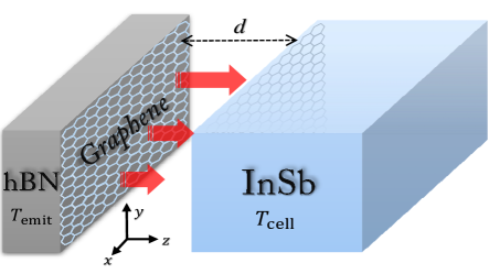
The proposed NTPV system is presented in Fig. 1. The emitter is a graphene covered h-BN film of thickness , kept at temperature . The TPV cell is made of an InSb - junction, kept at temperature , which is also covered by a layer of graphene. The thermal radiation from the emitter is absorbed by the cell and converted into electricity via infrared photoelectric conversion. In this system, plasmons in graphene can interact strongly with infrared photons and give rise to SPPs. Meanwhile, phonons in h-BN can also couple strongly with photons and leads to SPhPs Dai et al. (2014); Xu et al. (2014a); Brar et al. (2014); Kumar et al. (2015); Xu et al. (2014b); Woessner et al. (2015); Jiang et al. (2017). These emergent quasi-particles due to strong light-matter interaction can dramatically enhance thermal radiation, particularly via the near-field effect Brar et al. (2014); Kumar et al. (2015); Woessner et al. (2015); Zhao and Zhang (2015); Zhao et al. (2017); Shi et al. (2017). Because of their coincident frequency ranges, the SPPs and SPhPs hybrid with each other when graphene is placed together with h-BN, leading to hybrid polaritons called surface plasmon-phonon polaritons (SPPPs) Brar et al. (2014); Kumar et al. (2015). SPPPs have been shown to be useful in improving near-field heat transfer between two h-BN/graphene heterostructures Zhao and Zhang (2015); Zhao et al. (2017); Shi et al. (2017). The radiative heat transfer is optimized when the emitter and absorber are made of the same material, which leads to a resonant energy exchange between the emitter and the absorber Joulain et al. (2005). In order to enable such resonant energy exchange in our NTPV cell, we add another layer of graphene onto the InSb cell, as shown in Fig. 1.
The propagation of electromagnetic waves in these materials is described by the Maxwell equations, in which the dielectric functions of these materials are the key factors that determine the propagation of the electromagnetic waves. The dielectric function of h-BN is described by a Drude-Lorentz model, which is given by Kumar et al. (2015)
| (1) |
where denotes the out-of-plane and the in-plane directions, respectively. The in-(out-of-)plane direction is determined by whether the electric field is perpendicular (parallel) to the optical axis of the h-BN film (h-BN is a uniaxial crystal, and the optical axis is in the direction, as defined in Fig. 1). is the high-frequency relative permittivity, and are the transverse and longitudinal optical phonon frequencies, respectively. is the damping constant of the optical phonon modes. The values of these parameters are chosen as those determined by experiments Geick et al. (1966); Caldwell et al. (2014), , , and for in-plane phonon modes, , , and for out-of-plane phonon modes. There are certain frequency ranges where the in-plane and out-of-plane dielectric functions of h-BN have opposite signs, leading to the hyperbolicity of isofrequency contour, which makes h-BN a natural hyperbolic metamaterial Kumar et al. (2015).
The optical property of graphene sheet is described here by a modeled conductivity, , which sums over both the intraband and interband contributions, i.e., , given respectively by Falkovsky (2008)
| (2) |
and
| (3) |
where is a dimensionless function. is the chemical potential of the graphene sheet, which can be readily tuned via a gate-voltage Yan et al. (2013). is the electron scattering time and chosen as 100 fs in our calculations Woessner et al. (2015). is the temperature of the graphene sheet. , and are the electron charge, Boltzmann constant and the reduced Planck constant, separately.
The dielectric function of the InSb cell is given by Messina and Ben-Abdallah (2013)
| (4) |
where is the refractive index and is the speed of light in vacuum. is a step-like function which describes the absorption probability of the incident photons, and it is given by for and for with = 0.7 being the absorption coefficient and being the angular frequency corresponding to the band gap of InSb. The gap energy of InSb is temperature dependent, which is given by Shur (1996). For instance, for , the gap energy is nearly 0.17 eV and the corresponding frequency is about Hz.
The near-field radiative heat flux exchanged between the emitter and the cell is given by Polder and Van Hove (1971); Pendry (1999),
| (5) |
where , with and being the Planck mean oscillator energy of blackbody at temperature and , respectively. is the electrochemical potential difference across the - junction in the TPV cell. denotes the magnitude of the in-plane wavevector of thermal radiation waves and is called the photon transmission coefficient for the -polarization , which represents the probability for a photon with angular frequency and wavevector to tunnel through the vacuum gap from the emitter to the cell. The transmission coefficient for each polarization sums over the contribution from both propagating and evanescent waves Mulet et al. (2002),
| (6) |
where is the normal component of the wavevector in vacuum. and () are the reflection coefficients of the emitter and the cell, respectively, which measure the amplitude ratio between the reflected and incident waves at the interface of the emitter and the cell, respectively. These coefficients can be calculated by the scattering matrix approach where the optical interference in the heterostructure film is also taken into account Zhang (2007),
| (7) |
| (8) |
for s-polarization.
And
| (9) |
| (10) |
for p-polarization. Where 1, 2, and 3 are the indexes for the vacuum region above h-BN film, the h-BN film region, and the vacuum region below h-BN film,respectively, as defined in Ref. [Zhao and Zhang, 2015]. is the reflection coefficient between media and () for either or polarization, which is given by
| (11) | ||||
when there is a graphene layer in between media and ,
| (12) | ||||
when there is no graphene in between media and . Here and are the -component wavevectors for media for and polarization, respectively. and are the in-plane and out-of plane components of the relative dielectric tensor. For isotropic medium like vacuum and InSb, , and , where the dielectric function of the InSb cell is defined before. and are the permittivity and permeability for vacuum, respectively.
II.2 Characterizations of TPV cells
When the TPV cell is located at a distance which is on the order of or smaller than the thermal wavelength from the emitter, the radiative energy transfer will be enhanced due to the presence of evanescent waves Ilic et al. (2012), which exists only in the vicinity of the emitter, because of the exponential decay from the interface. The enhanced radiation with energy greater than the band gap will be absorbed by the TPV cell, creating electron-hole pairs and leading to electric current flow and output power generation. The induced electric current density can be written as Shockley and Queisser (1961); Ashcroft and Mermin (2010)
| (13) |
where is the voltage bias across the TPV cell, is a voltage which measures the temperature of the cell Shockley and Queisser (1961). and are called the photo-induced current density and reverse saturation current density, respectively. The reverse saturation current density (also named the dark current density, the electric current without light) is determined by the diffusion of minority carriers in the InSb - junction, which is given by
| (14) |
where is the intrinsic carrier concentration, which is dependent on the temperature of the TPV cell Shur (1996). and are temperature-dependent effective density of states in the conduction and valance bands, respectively given by and . and are the -region and -region impurity concentrations, respectively. Numerical values are set as . and are the diffusion coefficients of the electrons and holes, taken as and Lim et al. (2015). and are the relaxation times of the electron-hole pairs in the -region and -region, correspondingly. Values for relaxation times are calculated by Shur (1996).
Photo-induced current is the electric current induced by the motion of photo-carriers. The photo-induced current density is given by Laroche et al. (2006)
| (15) |
where the radiative spectral heat flux is defined in Sec. II.1. Here we assume that all incident photons are absorbed, and each photon with an energy greater than the band gap creates one electron-hole pair, i.e., we assume quantum efficiency Messina and Ben-Abdallah (2013). Under this assumption, we only consider the energy efficiency, which measures how much incident radiative heat can be transferred into electricity. We keep this assumption which is widely adopted in the literature.
The output electric power density is defined as the product of the net electric current density and the voltage bias,
| (16) |
and the energy efficiency is given by the ratio between the output electric power density and incident radiative heat flux ,
| (17) |
where the incident radiative heat flux is given by
| (18) |
III Results and Discussions
III.1 Performance of the designed NTPV systems
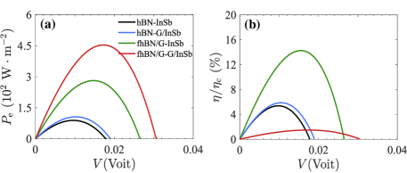
We first examine the electric power and the normalized energy efficiency in units of the Carnot efficiency () for our proposed near-field TPV cells. Fig. 2 shows the performances for the four different configurations, respectively denoted as hBN-InSb, hBN-G/InSb, fhBN/G-InSb, and fhBN/G-G/InSb. The electric power density and efficiency are calculated through Eq. (16) and (17), respectively. It is noted that by adding a single layer of graphene either on the emitter or the TPV cell, the output electric power density is considerably enhanced. Specifically, the enhancement factors of maximum electric power for fhBN/G-InSb cell (blue solid line) and hBN-G/InSb cell (green solid line) are respectively given by and . This enhancement induced by graphene (due to graphene SPPs) has been found in Ref. [Messina and Ben-Abdallah, 2013]. Notably, when the emitter and cell are both covered by graphene, the maximum electric power density is significantly enhanced, with the enhancement factor .


As indicated in Fig. 2(b), the energy efficiency also shows strong enhancement for hBN-G/InSb and fhBN/G-InSb cells, with the enhancement of the maximum efficiency and , respectively. While for fhBN/G-G/InSb cell, contrary to the considerable enhancement in output electric power, the energy efficiency for fhBN/G-G/InSb cell is substantially reduced.
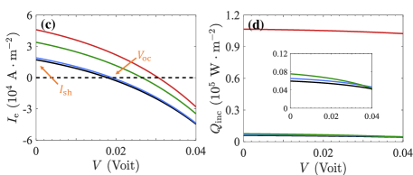
As shown in Fig. 2(c), the enhancement factors of short-circuit current densities (when the voltage bias is zero) for hBN-G/InSb, fhBN/G-InSb and fhBN/G-G/InSb cells are about , and , respectively. Besides, the enhancement factors of open-circuit voltage (when the electric current is zero) for the three covered cells are given by , and , respectively. The product of the short-circuit current and the open-circuit voltage gives a good estimation of the output power. Therefore, the enhancements of the short-circuit current and the open-circuit voltage lead to the significant improvement of the output power density shown in Fig. 2(a).
The different manifestation of energy efficiency for graphene-covered near-field systems can be interpreted by the competition between the electric power output and the radiative heat consumption. As shown in Fig. 2(d), the incident radiative heat flux (given by Eq. (18)) is increased , and for the hBN-G/InSb cell and fhBN/G-InSb cell, respectively. The enhancement of the output electric power exceeds the increase of the radiative heat consumption, leading to the improvement of energy efficiency. While for the fhBN/G-G/InSb cell, the radiative heat consumption is significantly increased , much higher than the improvement of the electric power output, leading to suppressed energy efficiency.
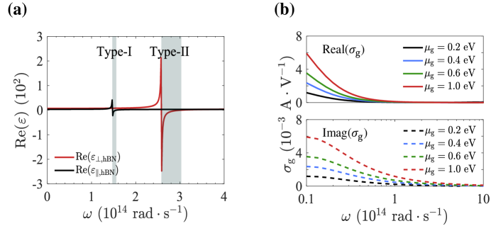
To figure out the microscopic mechanisms for the enhancement of the output power, we study the spectral distributions of the photo-induced current with the help of the dielectric function of h-BN and the optical conductivity of graphene. As shown in Fig. 3(a), two hyperbolic regions (labeled with type-I and type-II) are marked with gray shades. For type-I hyperbolicity, the corresponding frequency range is from (corresponding to the frequency of transverse phonon vibrations, ) to (corresponding to the frequency of longitudinal phonon vibrations, ). For type-II hyperbolicity, the corresponding frequency range is from ) to (corresponding to the frequency of longitudinal phonon vibrations, ). The sharp peaks shown in these two regions indicate the existence of SPhPs Jacob (2014); Geick et al. (1966). While in Fig. 3(b), the optical conductivities of graphene at various chemical potentials show the broadband nature of the graphene SPPs Yin et al. (2016).
The photo-induced current spectrum is given by Eq. (15) but integrated over only. As shown in Fig. 3(c), for hBN-InSb cell (black solid curve) the photo-induced current spectrum with a broad resonant peak is shown in the type-II hyperbolic regime (marked by the gray shade), which comes from the SPhPs. In hBN-G/InSb cell, the graphene sheet on InSb cell induces a resonant absorption between the emitter and the cell, depicted by the higher peak (blue solid curve), with about 20% increase compared with the hBN-InSb cell. Since near-field radiation is dominated by evanescent wave couplings between the emitter and the absorber, the resonant near-field absorption peak can be understood as due to the resonant coupling between the h-BN emitter and the InSb absorber. The resonant near-field absorption peak gives the major contribution to the photo-induced current and the output electric power.
Interestingly, there are two resonant peaks in the photo-induced current spectrum of the fhBN/G-InSb cell, separately labeled as 1 and 2 in the Fig. 3(c). And the corresponding frequencies are given by and , respectively. The low-frequency resonance and the broad high-absorption band in the type-II hyperbolic regime, are due to the hybrid polaritons named as the hyperbolic plasmon-phonon polaritons (HPPPs), which are resulted from the coupling between the SPPs in graphene and the SPhPs in h-BN in the type-II hyperbolic region Dai et al. (2014). The high-frequency absorption resonance outside the type-II region is due to the surface plasmon-phonon polaritons (SPPPs), which come from the strong coupling between the broadband graphene plasmons and the optical phonons outside the hyperbolic regions (i.e., regions without SPhPs) Kumar et al. (2015); Hajian et al. (2017). As a consequence, the photo-induced current is much larger and the bandwidth is much broader, which give rise to the major contribution in the photo-induced carrier generation and the electric power output. Further enhancement of the photo-induced carrier generation can be realized by adding a monolayer graphene to the InSb cell, as shown in Fig. 2(c).
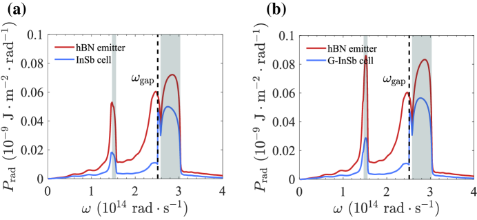
The incident radiative heat flux is examined in Fig. 3(d). The overall trends of are the same with the photo-induced current spectrums shown in Fig. 3(c). However, the incident radiative heat flux also includes the contributions from the below-band-gap near field heat transfer, which is quite different for the four configurations.
In order to understand the below-band-gap near field heat transfer, we present the near-field heat flux in a very large frequency range for both the emitter and the absorber in Fig. 4. The difference between the heat fluxes flowing out of the emitter and the absorber gives the radiative heat consumption, which consists of the useful part (above the InSb band gap) and the wasted part (below the InSb band gap). The band gap frequency of the InSb cell is marked by the black dashed line.
Comparing between Fig. 4(a) and Fig. 4(b), one can see that adding a graphene layer to the InSb cell increases both the useful and the wasted parts of the radiative heat flux, leading to slightly improved output power and energy efficiency. The best energy efficiency improvement comes from the configuration with a graphene layer added to the h-BN emitter. As shown in Fig. 4(c), for this configuration the useful part of the radiative heat flux is significantly increased, while the wasted heat flux is reduced. Therefore, the fhBN/G-InSb cell yields a significantly improved energy efficiency and output power. For the configuration with fhBN/G emitter and graphene-covered InSb junction, as shown in Fig. 4(d), the wasted radiative heat flux is dramatically increased. Although this configuration has the largest output power, the energy efficiency is the lowest among those four configurations.
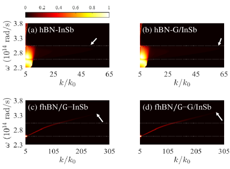
We further elaborate on the tunnel coupling between the emitter and the absorber by studying the photon tunneling probabilities (given by Eq. (6)) for the four configurations as shown in Fig. 5 for photons with frequency higher than the InSb band gap frequency, . The bright bands shown in Fig. 5 represent near photon tunneling probability, which originates from the strong coupling modes due to various surface polaritons. The angular frequency and wavevector of these strong coupling modes satisfy the efficient tunneling condition, i.e., the denominator of Eq. (6) is minimized. It is seen from Figs. 5(a) and 5(b) that with the bulk h-BN being the emitter, the high photon tunneling band is mainly provided by the Reststrahlen band of type-II hyperbolic phonon polaritons (the region between the two white dotted lines) with low wavevector. After integration over the wavevector , this narrow light band can only contribute to a small photo-induced current and limited output power. Adding a monolayer of graphene onto the InSb cell does not considerably improve the photo-induced current and the TPV performance. In contrast, when the h-BN/graphene heterostructure film serves as the emitter, the high photon tunneling band is no longer limited to the small wavevector region in the Reststrahlen band of type-II hyperbolic phonon polaritons. High photon tunneling extends to very large wavevector (the deep-subwavelength evanescent wave regime) and goes beyond the Reststrahlen band, as shown in Figs. 5(c) and 5(d), which leads to significantly increased phase space for high photon tunneling and hence considerably improved output power.
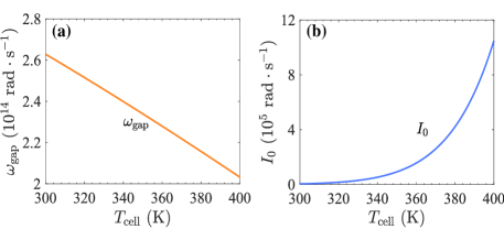
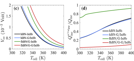
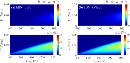
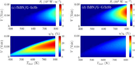
To understand the performances of the four NTPV configurations under different working temperatures, we study the band gap frequency, the reverse saturation current, the open-circuit voltage, and the absorption fraction of the incident thermal radiation as functions of the InSb junction temperature . As presented in Fig. 6(a), the InSb band gap frequency (orange solid curve) decreases from to when increases from 300 K to 400 K. Naively, one would expect that smaller band gap gives larger photon absorption flux and leads to better performances. Indeed, the photo-induced current increases considerably. However, the reverse saturation current increases exponentially with the cell temperature because of the reduction of the InSb band gap. As a consequence, the open-circuit voltages () are subsequently decreased, since is given by . The total outcome does not necessarily yield better performance.
Another important factor that dominates the energy efficiency is the absorption fraction, which is defined as the ratio of the radiative heat flux carried by photons with frequency higher than to the total absorbed heat flux, i.e., . The absorption fraction measures how much fraction of the absorbed heat flux is useful. It is seen from Fig. 6(d) that the absorption fractions for the four configurations are all increased with the temperature . Higher absorption fraction often leads to higher energy efficiency. It is reasonable to set the InSb cell temperature to 320 K which balances many different aspects. The corresponding band gap is 0.17 eV and the gap frequency is . At such a working temperature, the reverse saturation current density remains low, . Meanwhile, one can make good use of the incident photons, with the absorption fractions 0.80, 0.32, 0.31 and 0.043 for the hBN-InSb cell, hBN-G/InSb cell, fhBN/G-InSb cell, and fhBN/G-G/InSb cell, respectively. Under these circumstances, the TPV cells can make the most of the incident radiative heat and realize good performances, as shown in Fig. 2.
The best NTPV system should have resonant photon absorption right above the band gap Jiang and Imry (2018), which needs a fine matching between the emitter and the absorber. To the best of our knowledge, the fhBN/G-InSb configuration has the best thermophotovoltaic performances due to such matching.
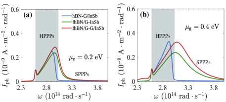
The near-field heat transfer can be strongly modified by the chemical potential of the graphene layer, . In Fig. 7, we plot the photo-induced current spectrums of the four different NTPV configurations with different . For the hBN-G/InSb cell, with large chemical potentials, the resonant peak in the HPPPs region of the photo-induced current spectrum is enhanced and split into small side peaks due to the resonant coupling with graphene plasmons. For the large chemical potential eV, the near field coupling between the SPhPs and the graphene plasmons is significantly enhanced. These behaviors are due to the dependence of the graphene plasmon frequencies on the chemical potential, as demonstrated in Refs. Dai et al., 2014, Xu et al., 2014b and Messina and Ben-Abdallah, 2013. The enhancement of photo-induced current spectrum by tuning provides an effective way to further enhance the performances of the graphene-based NTPV systems.
III.2 Optimization

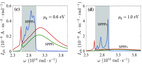
The output power and energy efficiency for the three configurations with graphene at four different chemical potentials are shown in Fig. 8. The output powers and energy efficiencies for these three configurations are all improved when the chemical potential of graphene is increased. Especially for the fhBN/G-G/InSb cell, the maximum output power density at eV is increased to nearly 6 times of that at eV. Meanwhile, the corresponding maximum efficiency is enhanced to 8.3 times of that at eV. For the hBN-G/InSb cell, the maximum output power density at eV is enhanced to about 12 times of that at eV, while the the corresponding maximum efficiency is enhanced to 1.6 times of that at eV. Also for the fhBN/G-InSb cell, the maximum output power density and maximum efficiency at higher chemical potential are enhanced to 2.5 and 1.4 times of those at eV, respectively. Such significant improvements of the TPV performances of the fhBN/G-InSb, hBN-G/InSb and fhBN/G-G/InSb cells are in accordance with the strongly enhanced photo-induced current spectrums shown in Fig. 7.
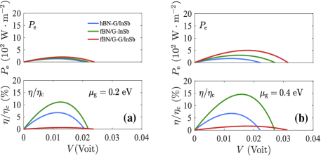
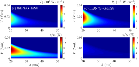
We also study the influence of the vacuum gap and the temperature of the emitter on the performances of four configurations, as shown in Figs. 9 and 10, respectively. The electric power density and the normalized energy efficiency are remarkably enhanced when the vacuum gap is reduced to 20 nm or when the emitter temperature is increased to 800 K. These results demonstrate that the near-field heat transfer is crucial for the enhancement of both the energy efficiency and the output power.
The optimal output power is achieved in the fhBN/G-G/InSb cell, with a power density of . The optimal efficiency, of the Carnot efficiency, is realized in the fhBN/G-InSb cell, while a moderate output power density is realized as well. Therefore, the best balance between the energy efficiency and the output power comes from the configuration with fhBN/G-InSb cell. The overall trend is that narrow vacuum gap, proper chemical potential of graphene, and high temperature of the emitter are favorable for high TPV performances.
IV Conclusions
We investigate the energy efficiency and output power of four different NTPV systems, denoted as the hBN-InSb cell, hBN-G/InSb cell, fhBN/G-InSb cell, and the fhBN/G-G/InSb cell, where the SPhPs in h-BN and graphene plasmons as well as their coupling play viable roles in enhancing the energy efficiency and power of these NTPV systems. It is found that the optimal output electric power with is achieved in hBN/graphene-graphene/InSb cell. While the optimal efficiency, of the Carnot efficiency, is reached in h-BN/graphene-InSb cell. The performance of the h-BN/graphene based cell can be further improved by tuning the chemical potential of graphene. Combining with the fact of the experimental availability of the h-BN/graphene heterostructure and the state-of-art doping of graphene Lu et al. (2017); Zhang et al. (2018), h-BN/graphene based cell can be useful for future thermophotovoltaic systems with high performances.
Remarkably, using such a graphene-BN-InSb near-field heterostructure design, we show that the performance of our NTPV systems can be comparable with the state-of-art thermoelectric systems working in the same temperature range. For instance, the state-of-art output power density of thermoelectric generators is realized in Ref.[ He et al., 2016] with a power factor (PF) W/m2 for a device working between two baths with temperatures K and K, whereas for the same conditions our NTPV device gives W/m2. The state-of-art device efficiency of thermoelectric generators is given in Ref.[ Zhao et al., 2016] where for a thermoelectric generator working between two thermal reservoirs with temperatures K and K. The corresponding device is . In comparison, for the same temperatures, our NTPV device can also give . These comparisons indicate that the NTPV systems have a high potential for future thermal to electric energy conversion.
V Acknowledgments
R.W., J.L., and J.-H.J. acknowledge support from the National Natural Science Foundation of China (NSFC Grant No. 11675116), the Jiangsu distinguished professor funding and a Project Funded by the Priority Academic Program Development of Jiangsu Higher Education Institutions (PAPD). R.W. thanks Professor Chen Wang for discussions.
References
- Shockley and Queisser (1961) W. Shockley and H. J. Queisser, J. Appl. Phys. 32, 510 (1961).
- Swanson (1980) R. M. Swanson, Thermophotovoltaic converter and cell for use therein (1980), uS Patent 4,234,352.
- Fraas et al. (1995) L. M. Fraas, J. E. Samaras, P. F. Baldasaro, and E. J. Brown, Spectral control for thermophotovoltaic generators (1995), uS Patent 5,403,405.
- Wojtczuk et al. (1995) S. Wojtczuk, E. Gagnon, L. Geoffroy, and T. Parodos (1995), vol. 321, pp. 177–187.
- Hamlen (1996) R. P. Hamlen, Thermophotovoltaic generator (1996), uS Patent 5,560,783.
- Coutts and Fitzgerald (1998) T. J. Coutts and M. C. Fitzgerald, Sci. Am. 279, 90 (1998).
- Martín and Algora (2004) D. Martín and C. Algora, Semicond. Sci. Tech. 19, 1040 (2004).
- Nagashima et al. (2007) T. Nagashima, K. Okumura, and M. Yamaguchi (2007), vol. 890, pp. 174–181.
- Fraas and Ferguson (2000) L. M. Fraas and L. G. Ferguson, Three-layer solid infrared emitter with spectral output matched to low bandgap thermophotovoltaic cells (2000), uS Patent 6,091,018.
- Sulima and Bett (2001) O. Sulima and A. Bett, Sol. Energ. Mat. Sol. C. 66, 533 (2001).
- Wu et al. (2012) C. Wu, B. Neuner III, J. John, A. Milder, B. Zollars, S. Savoy, and G. Shvets, J. Optics 14, 024005 (2012).
- Chan et al. (2013) W. R. Chan, P. Bermel, R. C. Pilawa-Podgurski, C. H. Marton, K. F. Jensen, J. J. Senkevich, J. D. Joannopoulos, M. Soljačić, and I. Celanovic, P. Nat. Acad. Sci. 110, 5309 (2013).
- Liao et al. (2016) T. Liao, L. Cai, Y. Zhao, and J. Chen, J. Power Sources 306, 666 (2016).
- Tervo et al. (2018) E. Tervo, E. Bagherisereshki, and Z. M. Zhang, Front. Energy 12, 5 (2018).
- Cravalho et al. (1967) E. G. Cravalho, C. L. Tien, and R. Caren, J. Heat Transfer 89, 351 (1967).
- Xu et al. (1994a) J. B. Xu, K. Lauger, K. Dransfeld, and I. H. Wilson, Rev. Sci. Instrum. 65, 2262 (1994a).
- Xu et al. (1994b) J. Xu, B. Koslowski, R. Möller, K. Läuger, K. Dransfeld, and I. H. Wilson, J. Vac. Sci. Technol. B 12, 2156 (1994b).
- Xu et al. (1994c) J. B. Xu, K. Läuger, R. Möller, K. Dransfeld, and I. H. Wilson, Appl. Phys. A 59, 155 (1994c).
- Xu et al. (1994d) J. B. Xu, K. Läuger, R. Möller, K. Dransfeld, and I. H. Wilson, J. Appl. Phys. 76, 7209 (1994d).
- Volokitin and Persson (2001) A. Volokitin and B. Persson, Phys. Rev. B 63, 205404 (2001).
- Mulet et al. (2002) J. P. Mulet, K. Joulain, R. Carminati, and J. J. Greffet, Microscale Thermophys. Eng. 6, 209 (2002).
- Hu et al. (2008) L. Hu, A. Narayanaswamy, X. Chen, and G. Chen, Appl. Phys. Lett. 92, 133106 (2008).
- Ilic et al. (2012) O. Ilic, M. Jablan, J. D. Joannopoulos, I. Celanovic, and M. Soljačić, Opt. Express 20, A366 (2012).
- Messina and Ben-Abdallah (2013) R. Messina and P. Ben-Abdallah, Sci. Rep. 3, 1383 (2013).
- Wang et al. (2012) B. Wang, X. Zhang, X. Yuan, and J. Teng, Appl. Phys. Lett. 100, 131111 (2012).
- Svetovoy et al. (2012) V. Svetovoy, P. Van Zwol, and J. Chevrier, Phys. Rev. B 85, 155418 (2012).
- Svetovoy and Palasantzas (2014) V. Svetovoy and G. Palasantzas, Phys. Rev. Appl. 2, 034006 (2014).
- Dai et al. (2014) S. Dai, Z. Fei, Q. Ma, A. S. Rodin, M. Wagner, A. S. McLeod, M. K. Liu, W. Gannett, W. Regan, K. Watanabe, et al., Science 343, 1125 (2014).
- Xu et al. (2014a) X. G. Xu, B. G. Ghamsari, J.-H. Jiang, L. Gilburd, G. O. Andreev, C. Zhi, Y. Bando, D. Golberg, P. Berini, and G. C. Walker, Nature Commun. 5, 4782 (2014a).
- Caldwell et al. (2014) J. D. Caldwell, A. V. Kretinin, Y. Chen, V. Giannini, M. M. Fogler, Y. Francescato, C. T. Ellis, J. G. Tischler, C. R. Woods, A. J. Giles, et al., Nature Commun. 5, 5221 (2014).
- Xu et al. (2014b) X. G. Xu, J.-H. Jiang, L. Gilburd, R. G. Rensing, K. S. Burch, C. Zhi, Y. Bando, D. Golberg, and G. C. Walker, Acs Nano 8, 11305 (2014b).
- Jiang and John (2014) J.-H. Jiang and S. John, Phys. Rev. X 4, 031025 (2014).
- Brar et al. (2014) V. W. Brar, M. S. Jang, M. Sherrott, S. Kim, J. J. Lopez, L. B. Kim, M. Choi, and H. Atwater, Nano Lett. 14, 3876 (2014).
- Kumar et al. (2015) A. Kumar, T. Low, K. H. Fung, P. Avouris, and N. X. Fang, Nano Lett. 15, 3172 (2015).
- Woessner et al. (2015) A. Woessner, M. B. Lundeberg, Y. Gao, A. Principi, P. Alonso-González, M. Carrega, K. Watanabe, T. Taniguchi, G. Vignale, M. Polini, et al., Nat. Materials 14, 421 (2015).
- Zhao and Zhang (2015) B. Zhao and Z. M. Zhang, J. Heat Transfer 139, 022701 (2015).
- Zhao et al. (2017) B. Zhao, B. Guizal, Z. M. Zhang, S. Fan, and M. Antezza, Phys. Rev. B 95, 245437 (2017).
- Shi et al. (2017) K. Shi, F. Bao, and S. He, ACS Photonics 4, 971 (2017).
- Heavens (1991) O. S. Heavens, Optical properties of thin solid films (Courier Corporation, 1991).
- Knittl (1976) Z. Knittl, Optics of thin films: an optical multilayer theory, vol. 1 (Wiley London:, 1976).
- Lim et al. (2015) M. Lim, S. Jin, S. S. Lee, and B. J. Lee, Opt. Express 23, A240 (2015).
- Jiang and Imry (2018) J.-H. Jiang and Y. Imry, Phys. Rev. B 97 (2018).
- Jiang et al. (2012) J.-H. Jiang, O. Entin-Wohlman, and Y. Imry, Phys. Rev. B 85, 075412 (2012).
- Jiang et al. (2013) J.-H. Jiang, O. Entin-Wohlman, and Y. Imry, Phys. Rev. B 87, 205420 (2013).
- Jiang (2014) J.-H. Jiang, J. Appl. Phys. 116, 194303 (2014).
- Entin-Wohlman et al. (2014) O. Entin-Wohlman, J.-H. Jiang, and Y. Imry, Phys. Rev. E 89, 012123 (2014).
- Jiang (2013) J.-H. Jiang, New J. Phys. 15, 075021 (2013).
- Jiang and Imry (2017) J.-H. Jiang and Y. Imry, Phys. Rev. Applied 7, 064001 (2017).
- Jiang et al. (2017) J.-H. Jiang, X. G. Xu, L. Gilburd, and G. C. Walker, Opt. Express 25, 25059 (2017).
- Joulain et al. (2005) K. Joulain, J.-P. Mulet, F. Marquier, R. Carminati, and J.-J. Greffet, Surf. Sci. Rep. 57, 59 (2005).
- Geick et al. (1966) R. Geick, C. Perry, and G. Rupprecht, Phys. Rev. 146, 543 (1966).
- Falkovsky (2008) L. A. Falkovsky, J. Phys.: Conference Series 129, 012004 (2008).
- Yan et al. (2013) H. Yan, T. Low, W. Zhu, Y. Wu, M. Freitag, X. Li, F. Guinea, P. Avouris, and F. Xia, Nat. Photonics 7, 394 (2013).
- Shur (1996) M. S. Shur, Handbook series on semiconductor parameters, vol. 1 (World Scientific, 1996).
- Polder and Van Hove (1971) D. Polder and M. Van Hove, Phys. Rev. B 4, 3303 (1971).
- Pendry (1999) J. Pendry, J. Phys.: Condens. Matter 11, 6621 (1999).
- Zhang (2007) Z. M. Zhang, Nano/microscale heat transfer (McGraw-Hill, 2007).
- Ashcroft and Mermin (2010) N. W. Ashcroft and N. D. Mermin, Google Scholar p. 461 (2010).
- Laroche et al. (2006) M. Laroche, R. Carminati, and J.-J. Greffet, J. Appl. Phys. 100, 063704 (2006).
- Jacob (2014) Z. Jacob, Nat. Mater. 13, 1081 (2014).
- Yin et al. (2016) G. Yin, J. Yang, and Y. Ma, Appl. Phys. Express 9, 122001 (2016).
- Hajian et al. (2017) H. Hajian, A. Ghobadi, S. A. Dereshgi, B. Butun, and E. Ozbay, JOSA B 34, D29 (2017).
- Lu et al. (2017) G. Lu, T. Wu, P. Yang, Y. Yang, Z. Jin, W. Chen, S. Jia, H. Wang, G. Zhang, J. Sun, et al., Adv. Sci. 4 (2017).
- Zhang et al. (2018) S. Zhang, J. Li, H. Wu, X. Li, and W. Guo, Adv. Mater. Interfaces 5, 1800208 (2018).
- He et al. (2016) R. He, D. Kraemer, J. Mao, L. Zeng, Q. Jie, Y. Lan, C. Li, J. Shuai, H. S. Kim, Y. Liu, et al., P. Natl. Acad. Sci. 113, 13576 (2016).
- Zhao et al. (2016) L.-D. Zhao, G. Tan, S. Hao, J. He, Y. Pei, H. Chi, H. Wang, S. Gong, H. Xu, V. P. Dravid, et al., Science 351, 141 (2016).