Current-phase relations of InAs nanowire Josephson junctions: from interacting to multi-mode regimes
Abstract
Gate-tunable semiconductor-superconductor nanowires with superconducting leads form exotic Josephson junctions that are a highly desirable platform for two types of qubits: those with topological superconductivity (Majorana qubits) and those based on tunable anharmonicity (gatemon qubits). Controlling their behavior, however, requires understanding their electrostatic environment and electronic structure. Here we study gated InAs nanowires with epitaxial aluminum shells. By measuring current-phase relations (CPR) and comparing them with analytical and numerical calculations, we show that we can tune the number of modes, determine the transparency of each mode, and tune into regimes in which electron-electron interactions are apparent, indicating the presence of a quantum dot. To take into account electrostatic and geometrical effects, we perform microscopic self-consistent Schrodinger-Poisson numerical simulations, revealing the energy spectrum of Andreev states in the junction as well as their spatial distribution. Our work systematically demonstrates the effect of device geometry, gate voltage and phase bias on mode behavior, providing new insights into ongoing experimental efforts and predictive device design.
Introduction
Studies of hybrid structures of superconductors and semiconducting nanowires have recently spurred advances in fundamental physics, materials science, and technology [1]. A growing body of experimental evidence supports proposals that nanowire-superconductor hybrids can host Majorana modes, the building blocks in schemes for topological quantum computing [2, 3, 4, 5, 6, 7, 8, 9, 10, 11, 12, 13]. Gate-tunable nanowire Josephson junctions have also been integrated into a cavity-QED architecture, providing electrostatic control of the qubit transition frequency [14, 15]. Improving the design and operation of these devices will rely on understanding their electrostatic environment and electronic structure, with several recent works examining mode behavior in wire devices [16, 17, 18, 19, 20, 21]. Moreover, electron-electron interactions, often overlooked in both experiment and theory, should also be considered as they are expected to play an important role, particularly in one or fewer dimensions.
Here we report measurements of the current-phase relation (CPR) of a Josephson junction based on an InAs nanowire, carried out using a scanning Superconducting QUantum Interference Device (SQUID) microscope. The amplitude and phase dependence of the CPR are sensitive to the transparency and number of modes contributing to supercurrent in the junction. Microscopic regimes with one or multiple modes can be distinguished through comparison to a simple analytic model, by a model-independent analysis, and by comparison to numerical simulations. The good agreement between our simulations and experiment provides a way to visualize the spatial arrangement of states in the wire and their response to electrostatic gating. In the regime of low electron density in the junction, we find evidence for interactions, which modify both the spectrum and the phase-dependence of current flow in the device (i.e., lead to a sign reversal of the supercurrent). Our simulation of the device behavior, combined with our understanding and control of both interactions and anharmonicity, provides new insight into recent experiments and allows for more deterministic device design.
Measuring the current-phase relation of an InAs nanowire Josephson junction
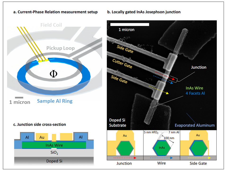
To investigate the CPR of the InAs nanowire Josephson junction, we fabricated a superconducting ring consisting of a 100 nm thick annular film of evaporated aluminum bridged by a hybrid epitaxial aluminum–InAs nanowire (Figure 1a). The Josephson junction is located at the center of the nanowire. To measure the current-phase relation, we positioned the pickup loop and field coil of a SQUID microscope approximately 1 micron above the sample ring [22]. When a current is applied to the field coil, a magnetic flux is generated in the sample ring. This flux directly tunes the phase difference across the nanowire junction, leading to a supercurrent in the junction due to its current-phase relation. The supercurrent circulates in the sample ring and is measured as a flux in the pickup loop [23, 24, 25]. By modeling the SQUID-sample geometry and calibrating the mutual inductance against the periodicity of the current-phase relation, we convert the flux signal into a Josephson supercurrent in the ring (See Supplemental Material I).
The hybrid nanowires are grown by Molecular Beam Epitaxy [26]. Au-catalyzed InAs nanowires are first grown via the vapor-liquid-solid method followed by a low temperature in-situ growth step of 7 nm aluminum on four of the six side facets (Figure 1b). The four facet coverage is realized in two steps of two-facet growth with an intermediate 120 degree rotation of the nanowire orientation with respect to the atomic aluminum beam, which ensures a flat continuous aluminum film on all four facets. This epitaxial aluminum makes electrical contact with the evaporated aluminum film to close the ring. In the center of the nanowire, the epitaxial aluminum is chemically removed over a span of 100-150 nm to form the junction. The junction lies under a Ti/Au “cutter” gate, while two additional side gates overlap the wire in regions still contacted with epitaxial aluminum (see Figure 1c). A 5 nm layer of HfO2 isolates the gates and the wire. The side gates are expected to be mostly screened by aluminum, but can still affect the wire via fringe electric fields. Finally, the sample ring sits on a doped silicon substrate capped with a thin layer of oxide, allowing the wire to be gated from below. We found that the cutter gate and back gate have qualitatively similar effects, indicating that both gates primarily affect the same junction region (under the cutter gate) due to screening from the epitaxial aluminum (See Supplemental Material II). Hence, we focus mainly on the modulation of the CPR by the cutter gate and side gates.
Evolution of the current-phase relation with the cutter gate voltage
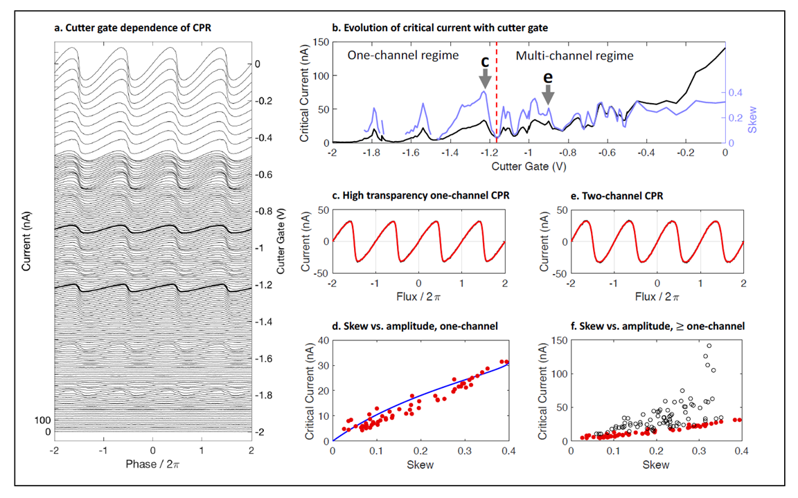
To explore the effect of local gating on the nanowire junction, we measured the CPR at a series of voltages applied to the cutter gate (Figure 2a). As the cutter gate voltage is tuned from to V, the amplitude of the CPR evolves through several qualitatively distinct regimes. At the most negative gate voltages, the onset of supercurrent gives way to a set of recurring peaks in the critical current (plotted in black in Figure 2b). As the gate voltage increases above V, the critical current begins to fluctuate with gate voltage. Finally, above V, the fluctuations diminish and the critical current begins to increase more steeply with gate voltage.
These gate-dependent features of the junction’s critical current are accompanied by strong variations in the phase dependence, or shape, of the CPR (visible in Figure 2a). The most prominent feature of these shape variations is their forward skew, meaning that the critical current occurs at an advanced phase compared to a sine wave. The skew of a CPR can be characterized by taking its Fourier transform and defining a quantity , where and are the first and second harmonics of the CPR. Positive indicates forward skew, and hereafter we use and ‘skew’ interchangeably.
Plotting the skew on the same gate voltage axis as the critical current reveals an intricate interplay between the shape of the CPR and its amplitude (light blue in Figure 2b). At the most negative gate voltages, recurring peaks in the critical current are accompanied by coincident peaks in the skew. In the intermediate regime of fluctuating critical current, the skew also fluctuates and some correlations are observable between critical current and skew. As the critical current begins to increase sharply at the most positive gate voltages, the skew remains relatively constant near . Throughout the gate trace, it is remarkable that almost never approaches . The CPR is nearly always forward-skewed, in sharp contrast with the sinusoidal behavior () found in the conventional Josephson effect. At certain gate voltages, the skew is not calculated due to the CPR amplitude being too small to obtain a reliable result.
Short junction theory and CPR skew reveal mode number and transparency
The variations of the CPR amplitude and shape with gate voltage contain considerable information about the electronic structure of the junction. The CPR depends on the electronic properties of the junction according to the fundamental relation
| (1) |
where is the free energy and is the phase difference across the Josephson junction [27]. In the limit where the junction length is short compared to the superconducting coherence length, the dominant contribution to the supercurrent comes from discrete spectrum of bound states in the junction, with energies [28]. The energies of these states, called Andreev bound states, are related to the transmission probabilities of the underlying normal conduction channels in the junction. Here is the proximity-induced gap. With this spectrum, Eq. (1) can be simplified to a well-known formula [29, 30, 31]:
| (2) |
Here corresponds to the number of Andreev bound states in the junction.
This simplified model illustrates that the CPR is a sensitive probe of both the number of modes and their transparencies. In the simplest case of a single channel, the amplitude and skew of the CPR both increase with . In the limit where , a sinusoidal CPR is expected (), while the maximum skew occurs for K and . When more than one channel contributes to the CPR, the shape and amplitude of the CPR become sensitive to a set of transmission probabilities.
We performed fits of Eq. (2) to the CPR data, allowing up to contributing modes (See Supplemental Material III for the fitting procedure). Below V, the CPR is well-described by a single contributing channel (dashed red line in Figure 2b). An example of a single-mode CPR with high skew, measured at V, is shown in black in Figure 2c. The best fit of Eq. (2) to the data, in red, is consistent with a single mode with and for .
In addition to fits, the single-channel regime is identified by a fixed relationship between the CPR amplitude and skew. As shown in blue in Figure 2d, calculated for and eV, increasing critical current corresponds to increased skew, up to the maximum skew . A scatter plot (red dots in Figure 2d) of data taken with the cutter gate voltage V shows that the critical current and skew are highly correlated as one would expect for a single channel. Experimentally this regime contains both the least and most skewed CPRs that we observed, with values as high as . The strong correlation between critical current and skew provides additional evidence for single-channel behavior.
Throughout the regime of fluctuating critical current, V to V, more channels contribute with fluctuating transmission probabilities. In Figure 2e, the measured CPR at V is plotted in black along with a best fit in red to Eq. (2) with modes. It is notable that the CPRs in Figure 2c and 2e have very similar amplitudes, but markedly different shapes, directly reflecting the contribution of multiple modes in Figure 2e. Hence, at V the best fit requires a minimum of two modes with transparencies and , whereas a single-mode fit is inconsistent with the experiment.
When more than one channel contributes to the CPR, there is no correlation between CPR amplitude and skew, in contrast with the single-channel regime. Instead, a range of critical currents are possible for a given value of the skew, with the single-channel behavior providing a lower bound. In Figure 2f, a scatter plot of skew and critical current data over the entire cutter gate range confirms this expectation: data where V (open black dots) occurs at larger critical currents than data where V. The lack of strong correlation between critical current and skew when V is evidence that this regime is characterized by multiple channels. The observed scatter captures the overall device behavior and constrains our numerical simulations, as we discuss below.
Above V, additional channels enter with transmission probabilities which increase rapidly with gate voltage. Interestingly, the CPR deviates from the short junction model at two of the peaks below V, which we discuss further below in the context of electron-electron interactions.
Using numerical simulations to study the interplay of electrostatic potential, spatial structure, and spectrum of Andreev states
Although the short junction model provides an intuitive description of the number and transparency of modes in the junction, it is limited in its ability to faithfully represent device behavior. In a real device, the spectrum and spatial distribution of states will be influenced by the device geometry, material composition, and details of the electrostatic potential [32, 33, 34]. Understanding these effects is important for device engineering in qubit and Majorana applications, motivating a more detailed model of the observed CPR.
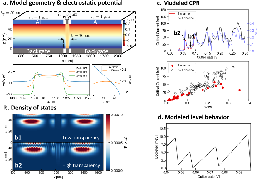
We study a microscopic model of the system, consisting of two wires and a junction, the geometry shown in the Figure 3a. The wire’s state is controlled by three electric gates: two below the wires and the cutter gate in the junction. In the normal state it is described by the following low-energy Hamiltonian
| (3) |
where operators denote the momentum in directions, are Pauli matrices, [1] is the effective mass in InAs ( being the electron mass), eVnm is the spin-orbit coupling [1] and is the electrostatic potential, created by the electric gates. The potential is translationally invariant along the direction and can be calculated solving the Poisson equation with and the boundary conditions set by the voltages of the surrounding gates and the band-offset at the interface of InAs and Al, which we take as eV. In order to obtain the potential one has to self-consistently determine density of electrons and the potential in a Schrodinger-Poisson loop, which is computationally prohibitive. Instead we employ the Thomas-Fermi approximation for the density which produces excellent agreement for the potential with the full Schrodinger-Poisson method [32, 35].
Superconductivity is included using a Bogoliubov-de-Gennes Hamiltonian and adding pairing potentials and to the left and right proximitized segments of the wires respectively, leading to the phase difference across the junction. The numerical complexity is alleviated by projecting the Hamiltonian in the direction to the basis of sinusoidal eigenstates [32, 36].
The zero-temperature CPR is calculated from the Andreev spectrum by taking the derivative of the ground state energy with respect to (see Eq. (1)) [37]. The gate dependence of the simulated critical current is shown in the upper panel of Figure 3c) (black), and is qualitatively similar to the experimental data. As the gate voltage increases, an insulating regime transitions into three well-separated peaks, which then evolve into a regime of fluctuating critical current. Within the regime of recurring peaks, the simulated supercurrent is dominated by the contribution from a single mode. The skew of the modeled CPR tends to increase and decrease with the critical current (light blue in Figure 3c). Plotting the simulated skews and critical currents against one another reveals that this relationship strongly resembles the experiment (lower panel in Figure 3c). The simulated behavior with only one contributing mode, plotted in red, shows strong correlation between critical current and skew. These single-channel points lie predominantly along the bottom part of the scatter plot, as found experimentally.
The excellent agreement between the measured and simulated CPRs provides an opportunity to further examine the electronic structure of the device. In Figure 3b, the local density of states in the single-channel regime reveals a striking difference in the structure of low and high transparency states. In both cases the band offset between aluminum and InAs leads to an enhanced density of states in the nanowire near the aluminum coating. At low transparency, the density of states in the junction area is low relative to that of the leads. In contrast, at high transparency the density of states becomes much larger in the junction. The change between regimes occurs in the range of mV difference in , indicating the delicate nature of the quantum states in the junctions formed by InAs nanowires.
Figure 3d shows the evolution with cutter gate voltage of highest occupied level energy in the junction, where zero energy corresponds to the chemical potential of the leads. This simulation demonstrates that sweeping the cutter gate voltage can be expected to bring a series of states in and out of resonance with the leads. In the single-channel regime in particular, this resonance behavior contributes to the formation of recurring peaks in the critical current.
Interacting behavior in the single-mode peaked regime
We now focus on the single-channel regime, to investigate in more detail the series of recurring peaks in critical current (Figure 4a). Near two of these peaks, the CPR deviates from the non-interacting behavior and instead displays a shoulder near phase (Figure 4b). When the cutter gate voltage is tuned away from the peaks, the shoulder feature is no longer observed (not shown, refer to Figure 2), and the CPR reverts back to a shape consistent with non-interacting short junction theory. The shoulder features are a precursor to -junction behavior resulting from Coulomb blockade effect[38, 39, 40, 41, 42, 43, 44, 45, 46], and have been studied experimentally in a carbon nanotube Josephson junction [47]. Related phenomena have also been observed in nanowire-superconductor hybrids [48, 49, 50, 51, 17], but without quantitative modeling of the CPR.
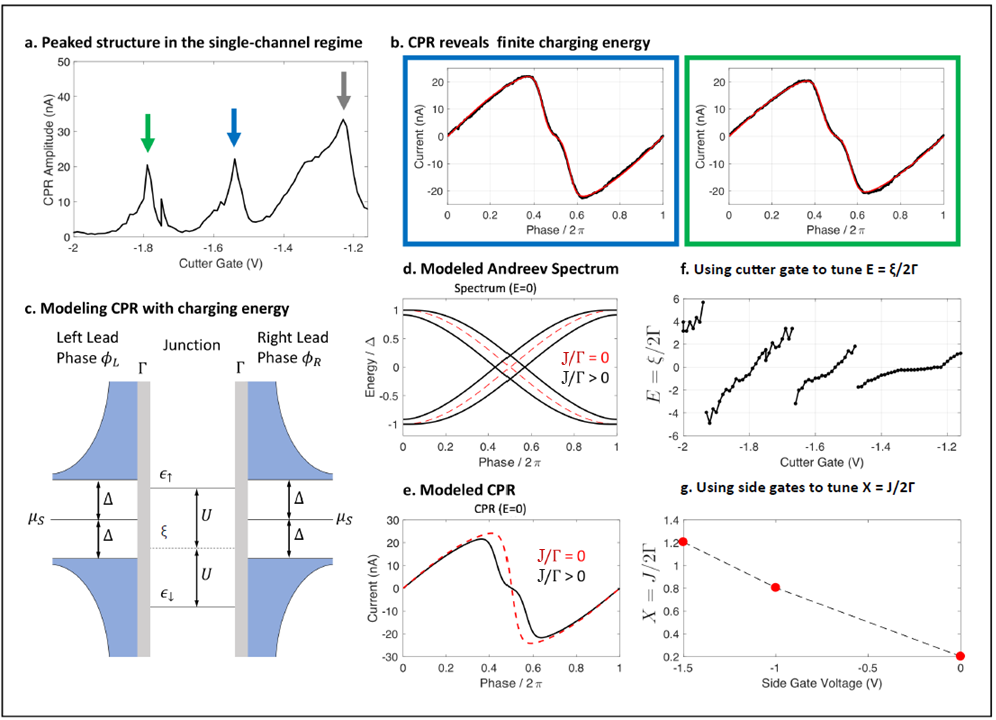
To understand the shoulder behavior in the CPR, we consider a scenario where a quantum dot (QD) is formed in the junction. The QD is characterized by the strength of the local Coulomb electron-electron interaction and a single spin-degenerate level with energy measured relative to the chemical potential of the leads (see Figure 4c). Coupling strengths to the right/left leads and the energy depend on the cutter gate voltage. Following Ref. [40] we treat interactions within the mean-field approximation and introduce a local exchange field where are single-level occupation probabilities for spin-up and spin-down electrons. In the limit when , the resulting Andreev energies can be obtained analytically:
| (4) |
Here is the phase difference between the left and right leads, , , , and . With the above formula for the Andreev spectrum, we have the following expression for the current-phase relation:
| (5) |
In this model, the expected junction behavior results from an interplay between the level energy and the on-site exchange coupling . The characteristics peaks in the supercurrent observed in the experiment, see Figure 4a, are related to the charge-degeneracy points. We now analyze CPR using a simple model above and consider case. Without interactions, such a situation corresponds to a resonant transmission through the QD with CPR given by the red line in Figure 4d. The exchange interactions effectively split spin-degenerate level creating level crossings away from (black curves in Figure 4d). Using this spectrum one finds the appearance of a shoulder near in CPR. By fitting the experimental data to the Eq. (5), we find a good agreement with the measured CPR data, with best fit values for the interaction strength given by and when V and V respectively (red dashed curve in Figure 4b is the best fit).
Away from the single-particle resonance (i.e. ), the dispersion of the Andreev states with gets suppressed due to the reduction in transmission probability through the QD. A nonzero exchange energy splits the Andreev level spin-degeneracy as before, but as long as the levels will not cross at zero energy. Thus, one expects the reversal of the supercurrent to appear in the CPR only when the junction is tuned near resonance. Indeed, we only observe shoulders in the CPR near peaks in the critical current, consistent with the theoretical predictions.
Fitting the measured CPR to Eq. (5) throughout the single-channel regime allows one to extract the cutter gate dependence of the normalized site energy, (Figure 4f). As the cutter gate increases from V to V, three levels are tuned in and out of resonance with the leads. In addition to shifting the spectrum, the cutter gate is expected to modify the shape of the confining potential in the junction and the coupling . We speculate that the coupling may increase with , contributing to the decrease in slopes in Figure 4f as becomes more positive. The experimentally extracted evolution of levels agrees qualitatively with numerical simulations (see Figure 3d).
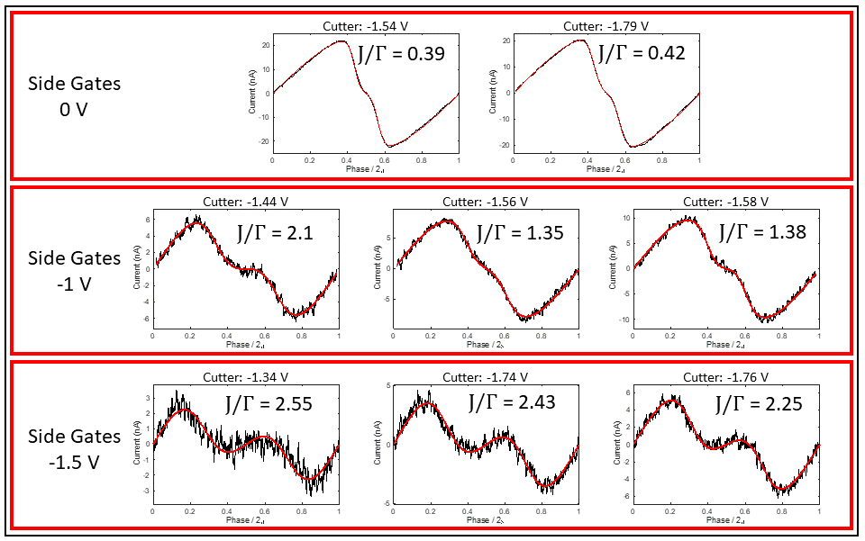
In the measurements discussed so far, only the cutter gate voltage was varied, with all other gates grounded. With negative voltage applied to the two side gates, we observed additional CPRs with shoulder-like features. Fitting these CPRs to Eq. (5) yielded values for the normalized exchange energy . As the side gate voltages become more negative, we find an increase in the mean value of at each gate voltage (Figure 4g and Supplemental Material II). Fringe electric fields at the two ends of the junction may lead to decreased coupling with more negative , consistent with this finding. We observed no shoulder-like features in any CPR with positive side gate voltage.
Conclusion
Our measurements and analysis distinguish between a multi-channel regime and a single-channel regime with widely tunable anharmonicity and interactions. Our CPR-based technique for comparing experiment and numerical simulations allows detailed study of the interplay between mode structure and electrostatics, and may be extended to the design and analysis of future superconductor-semiconductor heterostructures [52]. The propensity for quantum dot formation in a nanowire-based junction may also be viewed as a resource to detect Majorana modes. For example, a recent analysis found that -junction behavior occurs with a quantum dot between two conventional superconducting leads [50].
The presence of interactions at low electron density also has implications for experiments examining mode behavior in superconductor-nanowire hybrids, where interactions are sometimes neglected. For example, a recent work examined multiple Andreev reflections as a probe of transparency in few-mode junctions, but ignored interaction effects which are known to influence IV characteristics [18, 53]. Spectroscopy experiments also studied anharmonicity and Zeeman-induced spin-splitting of Andreev levels in the few-mode regime, but may also be affected by splitting effects from interactions as examined in our work [16, 19]. Overall our ability to accurately model device behavior, as well as to understand and control both interactions and anharmonicity, will elucidate the interpretation of current experiments and provide a method for device design.
References
- [1] Lutchyn, R. et al. Majorana zero modes in superconductor-semiconductor heterostructures. Nature Review Materials 3, 52–68 (2018).
- [2] Kitaev, A. Y. Unpaired Majorana fermions in quantum wires. Physics-Uspekhi 44, 131 (2001).
- [3] Lutchyn, R. M., Sau, J. D. & Das Sarma, S. Majorana fermions and a topological phase transition in semiconductor-superconductor heterostructures. Phys. Rev. Lett. 105, 077001 (2010). URL https://link.aps.org/doi/10.1103/PhysRevLett.105.077001.
- [4] Oreg, Y., Refael, G. & von Oppen, F. Helical liquids and majorana bound states in quantum wires. Phys. Rev. Lett. 105, 177002 (2010). URL https://link.aps.org/doi/10.1103/PhysRevLett.105.177002.
- [5] Mourik, V. et al. Signatures of Majorana fermions in hybrid superconductor-semiconductor nanowire devices. Science 336, 1003–1007 (2012).
- [6] Deng, M. et al. Anomalous zero-bias conductance peak in a Nb–InSb nanowire–Nb hybrid device. Nano Letters 12, 6414–6419 (2012).
- [7] Das, A. et al. Zero-bias peaks and splitting in an Al-InAs nanowire topological superconductor as a signature of Majorana fermions. Nature Physics 8, 887–895 (2012).
- [8] Rokhinson, L. P., Liu, X. & Furdyna, J. K. The fractional a.c. Josephson effect in a semiconductor-superconductor nanowire as a signature of Majorana particles. Nature Physics 8, 795–799 (2012).
- [9] Churchill, H. O. H. et al. Superconductor-nanowire devices from tunneling to the multichannel regime: Zero-bias oscillations and magnetoconductance crossover. Phys. Rev. B 87, 241401 (2013). URL https://link.aps.org/doi/10.1103/PhysRevB.87.241401.
- [10] Finck, A. D. K., Van Harlingen, D. J., Mohseni, P. K., Jung, K. & Li, X. Anomalous modulation of a zero-bias peak in a hybrid nanowire-superconductor device. Phys. Rev. Lett. 110, 126406 (2013). URL https://link.aps.org/doi/10.1103/PhysRevLett.110.126406.
- [11] Albrecht, S. M. et al. Exponential protection of zero modes in Majorana islands. Nature 531, 206–209 (2016).
- [12] Deng, M. et al. Majorana bound state in a coupled quantum-dot hybrid-nanowire system. Science 354, 1557–1562 (2016).
- [13] Zhang, H. et al. Quantized Majorana conductance. Nature 556, 74–79 (2018).
- [14] Larsen, T. W. et al. Semiconductor-nanowire-based superconducting qubit. Phys. Rev. Lett. 115, 127001 (2015). URL https://link.aps.org/doi/10.1103/PhysRevLett.115.127001.
- [15] de Lange, G. et al. Realization of microwave quantum circuits using hybrid superconducting-semiconducting nanowire josephson elements. Phys. Rev. Lett. 115, 127002 (2015). URL https://link.aps.org/doi/10.1103/PhysRevLett.115.127002.
- [16] van Woerkom, D. et al. Microwave spectroscopy of spinful Andreev bound states in ballistic semiconductor Josephson junctions. Nature Physics 13, 876–881 (2017).
- [17] Spanton, E. et al. Current-phase relations of few-mode InAs nanowire Josephson junctions. Nature Physics 13, 1177–1181 (2017).
- [18] Goffman, M. et al. Conduction channels of an InAs-Al nanowire Josephson weak link. New Journal of Physics 19, 092002 (2017).
- [19] Kringhøj, A. et al. Anharmonicity of a superconducting qubit with a few-mode josephson junction. Phys. Rev. B 97, 060508 (2018). URL https://link.aps.org/doi/10.1103/PhysRevB.97.060508.
- [20] Hays, M. et al. Direct microwave measurement of andreev-bound-state dynamics in a semiconductor-nanowire josephson junction. Phys. Rev. Lett. 121, 047001 (2018). URL https://link.aps.org/doi/10.1103/PhysRevLett.121.047001.
- [21] Tosi, L. et al. Spin-orbit splitting of andreev states revealed by microwave spectroscopy. Phys. Rev. X 9, 011010 (2019). URL https://link.aps.org/doi/10.1103/PhysRevX.9.011010.
- [22] Kirtley, J. R. et al. Scanning SQUID susceptometers with sub-micron spatial resolution. Review of Scientific Instruments 87, 093702 (2016).
- [23] Jackel, L. D., Buhrman, R. A. & Webb, W. W. Direct measurement of current-phase relations in superconducting weak links. Phys. Rev. B 10, 2782–2785 (1974). URL https://link.aps.org/doi/10.1103/PhysRevB.10.2782.
- [24] Sochnikov, I. et al. Direct measurement of current-phase relations in superconductor/topological insulator/superconductor junctions. Nano Letters 13, 3086–3092 (2013).
- [25] Sochnikov, I. et al. Nonsinusoidal current-phase relationship in josephson junctions from the 3d topological insulator hgte. Phys. Rev. Lett. 114, 066801 (2015). URL https://link.aps.org/doi/10.1103/PhysRevLett.114.066801.
- [26] Krogstrup, P. et al. Epitaxy of semiconductor–superconductor nanowires. Nature Materials 14, 400–406 (2015).
- [27] Beenakker, C. W. J. & van Houten, H. The superconducting quantum point contact. In Proceedings of the International Symposium on Nanostructures and Mesoscopic Systems, 481–497 (Academic Press, Inc., 1992).
- [28] Beenakker, C. W. J. Universal limit of critical-current fluctuations in mesoscopic josephson junctions. Phys. Rev. Lett. 67, 3836–3839 (1991). URL https://link.aps.org/doi/10.1103/PhysRevLett.67.3836.
- [29] Kulik, I. & Omelyanchuk, A. Contribution to the microscopic theory of the Josephson effect in long superconducting junctions. Zh. Eksp. Teor. Fiz. Piz. Red. 21, 216–219 (1975).
- [30] Haberkorn, W., Knauer, H. & Richter, J. A theoretical study of the current-phase relation in Josephson contacts. Physica Status Solidi (a) 47, K161–K164 (1978).
- [31] Zaĭtsev, A. Quasiclassical equations of the theory of superconductivity for contiguous metals and the properties of constricted microcontacts. Zh. Eksp. Teor. Fiz. Piz. Red. 86, 1742–1758 (1984).
- [32] Antipov, A. E. et al. Effects of gate-induced electric fields on semiconductor majorana nanowires. Phys. Rev. X 8, 031041 (2018). URL https://link.aps.org/doi/10.1103/PhysRevX.8.031041.
- [33] Woods, B. D., Stanescu, T. D. & Das Sarma, S. Effective theory approach to the schrödinger-poisson problem in semiconductor majorana devices. Phys. Rev. B 98, 035428 (2018). URL https://link.aps.org/doi/10.1103/PhysRevB.98.035428.
- [34] Winkler, G. W. et al. A unified numerical approach to semiconductor-superconductor heterostructures. ArXiv e-prints (2018). 1810.04180.
- [35] Mikkelsen, A. E. G., Kotetes, P., Krogstrup, P. & Flensberg, K. Hybridization at superconductor-semiconductor interfaces. Phys. Rev. X 8, 031040 (2018). URL https://link.aps.org/doi/10.1103/PhysRevX.8.031040.
- [36] Stanescu, T. D., Lutchyn, R. M. & Das Sarma, S. Majorana fermions in semiconductor nanowires. Phys. Rev. B 84, 144522 (2011). URL https://link.aps.org/doi/10.1103/PhysRevB.84.144522.
- [37] Cheng, M. & Lutchyn, R. M. Josephson current through a superconductor/semiconductor-nanowire/superconductor junction: Effects of strong spin-orbit coupling and zeeman splitting. Phys. Rev. B 86, 134522 (2012). URL https://link.aps.org/doi/10.1103/PhysRevB.86.134522.
- [38] Spivak, B. I. & Kivelson, S. A. Negative local superfluid densities: The difference between dirty superconductors and dirty bose liquids. Phys. Rev. B 43, 3740–3743 (1991). URL https://link.aps.org/doi/10.1103/PhysRevB.43.3740.
- [39] Rozhkov, A. V. & Arovas, D. P. Josephson coupling through a magnetic impurity. Phys. Rev. Lett. 82, 2788–2791 (1999). URL https://link.aps.org/doi/10.1103/PhysRevLett.82.2788.
- [40] Vecino, E., Martín-Rodero, A. & Yeyati, A. L. Josephson current through a correlated quantum level: Andreev states and junction behavior. Phys. Rev. B 68, 035105 (2003). URL https://link.aps.org/doi/10.1103/PhysRevB.68.035105.
- [41] Siano, F. & Egger, R. Josephson current through a nanoscale magnetic quantum dot. Phys. Rev. Lett. 93, 047002 (2004). URL https://link.aps.org/doi/10.1103/PhysRevLett.93.047002.
- [42] Choi, M.-S., Lee, M., Kang, K. & Belzig, W. Kondo effect and josephson current through a quantum dot between two superconductors. Phys. Rev. B 70, 020502 (2004). URL https://link.aps.org/doi/10.1103/PhysRevB.70.020502.
- [43] Sellier, G., Kopp, T., Kroha, J. & Barash, Y. S. junction behavior and andreev bound states in kondo quantum dots with superconducting leads. Phys. Rev. B 72, 174502 (2005). URL https://link.aps.org/doi/10.1103/PhysRevB.72.174502.
- [44] Karrasch, C., Oguri, A. & Meden, V. Josephson current through a single anderson impurity coupled to bcs leads. Phys. Rev. B 77, 024517 (2008). URL https://link.aps.org/doi/10.1103/PhysRevB.77.024517.
- [45] Meng, T., Florens, S. & Simon, P. Self-consistent description of andreev bound states in josephson quantum dot devices. Phys. Rev. B 79, 224521 (2009). URL https://link.aps.org/doi/10.1103/PhysRevB.79.224521.
- [46] Kiršanskas, G., Goldstein, M., Flensberg, K., Glazman, L. I. & Paaske, J. Yu-shiba-rusinov states in phase-biased superconductor–quantum dot–superconductor junctions. Phys. Rev. B 92, 235422 (2015). URL https://link.aps.org/doi/10.1103/PhysRevB.92.235422.
- [47] Delagrange, R. et al. Manipulating the magnetic state of a carbon nanotube josephson junction using the superconducting phase. Phys. Rev. B 91, 241401 (2015). URL https://link.aps.org/doi/10.1103/PhysRevB.91.241401.
- [48] Chang, W., Manucharyan, V. E., Jespersen, T. S., Nygård, J. & Marcus, C. M. Tunneling spectroscopy of quasiparticle bound states in a spinful josephson junction. Phys. Rev. Lett. 110, 217005 (2013). URL https://link.aps.org/doi/10.1103/PhysRevLett.110.217005.
- [49] Lee, E. et al. Spin-resolved Andreev levels and parity crossings in hybrid superconductor-semiconductor nanostructures. Nature Nanotechnology 9, 79–84 (2014).
- [50] van Dam, J., Nazarov, Y., Bakkers, E., De Franceschi, S. & Kouwenhoven, L. Supercurrent reversal in quantum dots. Nature 442, 667–670 (2006).
- [51] Szombati, D. B. et al. Josephson -junction in nanowire quantum dots. Nature Physics 12, 568–572 (2016).
- [52] Vaitiekėnas, S. et al. Selective-area-grown semiconductor-superconductor hybrids: A basis for topological networks. Phys. Rev. Lett. 121, 147701 (2018). URL https://link.aps.org/doi/10.1103/PhysRevLett.121.147701.
- [53] Avishai, Y., Golub, A. & Zaikin, A. Quantum dot between two superconductors. Europhysics Letters 54, 5 (2001).
- [54] Rosa, E. B. & Grover, F. W. Formulas and Tables for the Calculation of Mutual and Self Inductance. (Revised.), vol. 1(1/2) (The Washington Academy of Sciences, 1911).
- [55] Brandt, E. H. Thin superconductors and squids in perpendicular magnetic field. Phys. Rev. B 72, 024529 (2005). URL https://link.aps.org/doi/10.1103/PhysRevB.72.024529.
- [56] Vaitiekėnas, S., Deng, M.-T., Nygård, J., Krogstrup, P. & Marcus, C. M. Effective factor of subgap states in hybrid nanowires. Phys. Rev. Lett. 121, 037703 (2018). URL https://link.aps.org/doi/10.1103/PhysRevLett.121.037703.
- [57] Bevington, P. & Robinson, D. Data Reduction and Error Analysis for the Physical Sciences. McGraw-Hill Higher Education (McGraw-Hill Education, 2003). URL https://books.google.com/books?id=0poQAQAAIAAJ.
Acknowledgement
We thank S. Vaitiekėnas, J. Kirtley and G. Winkler for useful discussions. The scanning SQUID measurements were supported by the Department of Energy, Office of Basic Energy Sciences, Division of Materials Sciences and Engineering, under Contract No. DE-AC02-76SF00515. Nanowire growth and device fabrication was supported by Microsoft Project Q, the Danish National Research Foundation, the Lundbeck Foundation, the Carlsberg Foundation, and the European Research Commission through starting grant HEMs-DAM, grant no.716655. S. Hart acknowledges support from the GLAM Postdoctoral Fellowship at Stanford University. C.M. Marcus acknowledges support from the Villum Foundation.
Supplemental Material
I Estimating the Amplitude of the Critical Current
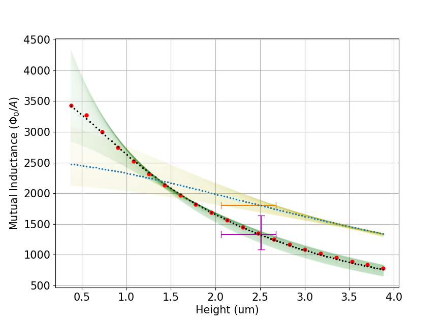
The advantage of having a flux-coupled measurement (being contact-less) of the Josephson current-phase relation also comes with the drawback of lacking a direct measurement of the amplitude of the current. In order to convert the measured flux signal into a phase-dependent Josephson current, we model the SQUID-sample geometry to the best of our knowledge to obtain the mutual inductance between the sample ring and the SQUID pickup loop.
First we apply a current into the SQUID field coil to introduce a phase drop of across the Josephson junction. is the mutual inductance between the sample ring and the SQUID field coil, set by the measurement geometry between the SQUID and the sample. is the superconducting flux quantum. We estimate the kinetic inductance of the Josephson junction to be much smaller than the self-inductance of the sample ring. Therefore, the persistent current due to fluxoid quantization is small, and thus the preceding equation is valid. Since the measured signal must be -periodic and is known, we can easily extract from the data.
The phase drop across the Josephson junction leads to a supercurrent that we inductively measure. The measured signal in the pickup loop is related to the actual supercurrent by = . To estimate , we model the field coil, pickup loop and sample ring as three coaxial 1-dimensional circles. The distance between the field coil and pickup loop is fixed to be 280 nm from the fabrication process [22]. The distance from the sample to the pickup loop is unknown and estimated to be 1.6 m. Using Maxwell’s analytic formula for two coaxial circles we can calculate the pair-wire mutual inductance [54]:
| (6) | ||||
Where is the vacuum permeability, and are the radii of the two circles, is the distance between their centers, K and E are respectively the complete elliptic integrals of the first and second kind with modulus k.
To compute the pair-wise mutual inductance at various heights (black and blue dotted lines in Figure S1), we use the effective radii of each superconducting annulus defined by . The calculated is also found to be in very good agreement with a thin film superconductor model (red dots) [55]. Using an experimentally extracted = 1800 , we find the real height to be 2.5 m (0.9 m off from the nominal height probably due to obsolete scanner calibration). To take into account the systematic uncertainty in the current distribution in the field coil and sample ring, we also compute the range of mutual inductance resulting from any arbitrary current distribution in the field coil and the sample ring (yellow and green bands respectively in Figure S1). Subsequently we obtain an uncertainty in height at = 1800 (orange error bar in Figure S1). We project the height uncertainty onto and obtain a range 1100 1600 . Additionally, off-axial alignment can give 10 of uncertainty in . We have processed the data in this paper with = 1170 , within the range of our systematic uncertainty and consistent with previous scanning SQUID measurements [17, 24, 25].
II Effects of Different Electrostatic Gates
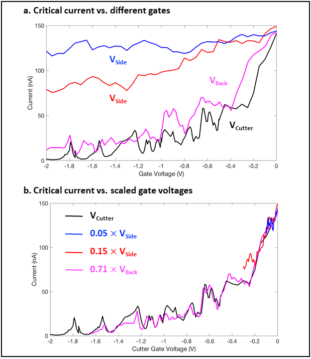
We measure current-phase relation as a function of each of the four electrostatic gates fabricated on the device (two side gates, one cutter gate and one back gate, as shown in Figure 1). We find that all four gates have different effects on the evolution of the CPR amplitude (shown in Figure S2a). When we scale the back gate voltages by an arbitrary factor of 0.71, we see that the effect of the back gate is qualitatively similar to that of the cutter gate (Figure S2b). We speculate that the epitaxial aluminum shell screens the electric field everywhere along the wire except the junction region, resulting in the back gate having the same effect on the juntion behavior as the cutter gate. On the other hand, the two side gates only cover parts of the wire with epitaxial aluminum, thus are strongly screened and cannot fully deplete the junction region (see Figure S2a and b). The observation of different gating behavior signifies the importance of understanding the spatial structure of the electrostatic potential and the bound states, an issue we address by numerical simulations of the device geometry in the main text. Even though the side gates do not effectively deplete electrons in the junction region, they affect the tunneling rates onto the junction in the interacting regime. Figure S3 shows the effect of both the side gate voltage and the cutter gate voltage on the normalized exchange energy . The electric field directly underneath the side gates are expected to be screened by the epitaxial aluminum, but the fringe electric fields creeping around the ends of the junction may lead to the systematic suppression of the tunneling rate at negative side gate voltages as seen in the experiment. Future device design may deliberately place finger gates over the two ends of the Josephson junction to further explore the interacting behavior.
III Model Fitting in the Single- and Multi-Channel Regime
We use the “fit()” function in MATLAB to perform a least-squares fit of the experimental data to the short-junction current-phase relation formula (2) in order to extract the number of independent channels and the corresponding transmission coefficients.
We first use a one-channel model with 3 free parameters , respectively the superconducting gap in the leads, the temperature, and the transmission coefficient as defined in Eq. (2), to fit the most skewed CPR at VC = 1.22 V (see main text Figure 2c). The high quality single-mode fit yields = 1, = 128 eV and T = 98 mK. We then use a two-channel fit with 4 free parameters to fit the same data. For the two-channel fit, the 95 confidence interval constricts 0.01. Therefore we conclude that only one channel is contributing to the supercurrent at VC = 1.22 V. Fitting this single perfectly transmitting channel yields very constrained values of and T, with 95 confidence intervals of 2 eV and 2 mK respectively, hence we fix = 128 eV and T = 98 mK for subsequent multi-channel fits. Notice that = 128 eV is smaller than the expected gap from 7 nm of epitaxial aluminum film [12, 56]. This can be explained by the inability of the back gate to deplete the wires of electrons, which would make it easier to proximitize to the superconductor [32], as well as large systematic amplitude uncertainty as shown in Supplemental Material I, in addition to effects from the evaporated (disordered) bulk aluminum ring.
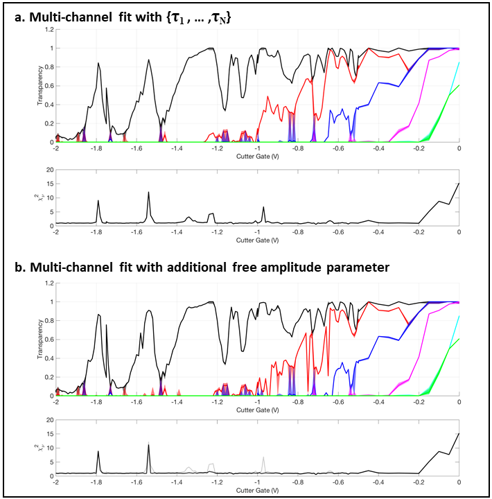
For N-channel fits, we manually set the number of channels in the fit through N = 1, 2, 3 … and use N free parameters to perform the least-squares fit to Eq. (2) at each value of N. The condition for the best fit is met when additional channels do not improve the fit quality, as measured by the residuals. The fitted transmission coefficients over the entire cutter gate voltage range is shown in Figure S4. 68 confidence intervals for the fit parameters are calculated from standard contour plots [57]. The confidence intervals (i.e. error bars) for each fitted transmission coefficient is shaded in Figure S2a. Notice these error bars only represent the statistical uncertainties in the fits and not the systematic uncertainties in the experiment.
Here we find our data to be consistent with up to 6 independent channels according to the short-junction theory. Below VC = 1.16 V, the CPR is dominated by a single channel. As VC becomes more positive, more channels are introduced and their transparencies fluctuate until VC 0.4 V, above which both the transparencies and the overall CPR amplitude monotonically increase towards positive cutter gate voltages.
To further validate our analysis, we calculate the reduced chi-squared () statistic as a test for goodness-of-fit [57]. The reduced chi-squared statistic is defined as the following:
| (7) |
where is the chi-squared statistic, is the variance of the experimental noise distribution, is the measured data. In this case it is the measured Josephson current at each phase bias. is the theoretical model value. In this case it is the theoretical Josephson current at each phase bias given by Eq. 2. is the degree of freedom of the fit, given by , where is the total number of data points and is the number of fit parameters.
If the data consists of a known theoretical model with free parameters plus Gaussian-distributed experimental noise, a set of best-fit parameters should result in , indicating that the data is well-described by the fitted model. Our measured SQUID noise floor, in units of the Josephson current from a ring, indeed follows a Gaussian distribution with variance of 1 (nA)2, which we use as an estimator for in Eq. 7. Using the residuals from the fits, the SQUID noise floor and the number of fit parameters, we calculate at each cutter gate voltage. The vast majority of our fits result in , indicating that the data is highly consistent with the short-junction model with independent channels (Figure S4a).
IV Deviations of the Fit from the Short-Junction Model
At a few values of gate voltage, we find that , indicating that the data cannot be fully described by the non-interacting short-junction model. Near peak transparency () in the single-channel regime, the charging energy modifies the shape of the CPR as shown in Figure 4b and Figure S3, thus resulting in bad fits to the non-interacting model (Eq. 2). For VC > 0.2 V, more channels (> 4) begin to participate in the Josephson current, potentially causing the independent-channel assumption in the model to breakdown, resulting also in large . In addition, we notice that between VC = 1.36 V and VC = 0.95 V, the indicates poor fit quality that is not clearly related to charging energy or interacting channels.
We revisit our multi-channel fit with an additional free amplitude parameter (a prefactor close to 1 that scales the amplitude of the supercurrent) and obtain improved fit quality as indicated by (Figure S4b). We interpret the remaining large peaks in as due to either charging energy or multi-channel interactions. Although the free amplitude parameter, which varies up to 10%, is equivalent to a changing , We are reluctant to consider this a measurement of a gate-voltage dependent superconducting gap. Weak interactions and geometric effects can cause subtle deviations in the shape of the CPR from the short-junction theory. In particular, the real device consists of proximitized superconducting leads, forming an S-S’-N-S’-S junction (where S refers to the bulk aluminum, S’ refers to InAs nanowire proximitized by the epitaxial aluminum shell, N refers to InAs nanowire without the epitaxial aluminum shell). In such a case, the spatial distribution of the eigenstates in the nanowire affects the superconductivity. Though absent in conventional SNS short-junction theories, this important aspect of the device is directly captured in our numerical modeling, which helps to illuminate the voltage dependence of mode behavior in our data.