A unified numerical approach to topological semiconductor-superconductor heterostructures
Abstract
We develop a unified numerical approach for modeling semiconductor-superconductor heterostructures. All the key physical ingredients of these systems — orbital effect of magnetic field, superconducting proximity effect and electrostatic environment — are taken into account on equal footing in a realistic device geometry. As a model system, we consider indium arsenide (InAs) nanowires with epitaxial aluminum (Al) shell, which is one of the most promising platforms for Majorana zero modes. We demonstrate qualitative and quantitative agreement of the obtained results with the existing experimental data. Finally, we characterize the topological superconducting phase emerging in a finite magnetic field and calculate the corresponding topological phase diagram.
I Introduction
The simulation of realistic quantum devices represents a challenging problem in computational physics, due to the difficulty of reaching quantitative agreement with experimental data on the basis of effective empirical models. The complexity of the problem is particularly demanding in the case of hybrid superconductor-semiconductor devices, which are promising platforms for realizing Majorana zero modes Kitaev (2001); Moore and Read (1991); Nayak and Wilczek (1996); Read and Green (2000); Ivanov (2001); Sau et al. (2010); Alicea (2010); Lutchyn et al. (2010); Oreg et al. (2010); Nayak et al. (2008); Alicea (2012); Beenakker (2013); Leijnse and Flensberg (2012); Das Sarma et al. (2015); Lutchyn et al. (2018); Aguado (2017), since semiconductors and superconductors (i.e. metals) are described by disparate characteristic length scales, effective masses, and electron densities. Furthermore, recent material science improvements of the semiconductor-superconductor interface Krogstrup et al. (2015); Lutchyn et al. (2018), due to the in-situ deposition of Al on InAs nanowire facets, reached the strong tunneling regime between the two materials Chang et al. (2015); Deng et al. (2016); Nichele et al. (2017); Zhang et al. (2018); Vaitiekėnas et al. (2018a). In this regime Stanescu et al. (2011), the wave functions of superconducting and semiconducting states are strongly hybridized due to the large coupling at the materials’ interface. The physical parameters required to describe the semiconducting material in simple effective models Lutchyn et al. (2010); Oreg et al. (2010) – e.g., proximity-induced pairing, -factor and spin-orbit coupling strength – are strongly renormalized by such a hybridization Cole et al. (2015); Sticlet et al. (2017); Antipov et al. (2018); Mikkelsen et al. (2018); Reeg et al. (2018). Thus, in order to understand physical properties of such a hybrid system, one has to develop a comprehensive numerical approach which takes into account different competing physical effects on equal footing. The development of appropriate device simulations carrying out this task is crucial for topological quantum computing proposals Das Sarma et al. (2015); Lutchyn et al. (2018) which rely on good control of Majorana zero modes.
In this paper, we develop a unified numerical approach for modeling of the semiconductor-superconductor heterostructures. Our approach appropriately takes into account the proximity-induced superconductivity in the strong tunneling limit, the orbital and Zeeman effect of an applied magnetic field, and the spin-orbit coupling, all within a self-consistent treatment of the electrostatic environment in the Thomas-Fermi approximation and in a realistic geometry. The simultaneous treatment of these ingredients was not achieved in previous numerical works to date Stanescu et al. (2011); Prada et al. (2012); Rainis et al. (2013); Cole et al. (2015); Nijholt and Akhmerov (2016); Reeg et al. (2017); Sticlet et al. (2017); Reeg et al. (2018); Dmytruk et al. (2018), which relied on effective phenomenological models neglecting the treatment of electrostatics and/or assuming the weak tunneling limit at the semiconductor-superconductor interface. Several recent works developed Schrödinger-Poisson calculations for proximitized nanowires Vuik et al. (2016); Antipov et al. (2018); Mikkelsen et al. (2018); Woods et al. (2018); Domínguez et al. (2017); Escribano et al. (2018), crucial for understanding electrostatics and gating effects, but they similarly neglected some of the other key ingredients listed above (most notably, the orbital effect of the magnetic field). The present approach builds on the recently improved treatment of electrostatic effects in the strong tunneling limit Antipov et al. (2018); Mikkelsen et al. (2018), incorporating the orbital effect of the magnetic field Nijholt and Akhmerov (2016); Winkler et al. (2017) as well as the dependence of the spin-orbit coupling on the external electric field. We demonstrate that such a unified treatment is crucial for a better understanding of the large body of existing experimental data Mourik et al. (2012); Rokhinson et al. (2012); Deng et al. (2012); Churchill et al. (2013); Das et al. (2012); Finck et al. (2013); Albrecht et al. (2016); Gül et al. (2018); Chen et al. (2017); Deng et al. (2016); Suominen et al. (2017); Nichele et al. (2017); Gazibegovic et al. (2017); Zhang et al. (2018, 2017); Sestoft et al. (2018); Deng et al. (2018); Vaitiekėnas et al. (2018a); Laroche et al. (2019); Chang et al. (2015); de Moor et al. (2018); Shen et al. (2018).
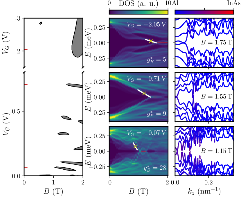
Tunneling conductance experiments Chang et al. (2015); Deng et al. (2016); Nichele et al. (2017); Vaitiekėnas et al. (2018a); de Moor et al. (2018) on InAs/Al Krogstrup et al. (2015) and InSb/Al Gazibegovic et al. (2017) hybrid nanowires show that the high-quality epitaxial semiconductor-superconductor interface translates into a proximity-induced gap comparable to that of bulk Al, with very small sub-gap conductance at zero magnetic field. These findings are evidence of the strong coupling between the two materials Stanescu et al. (2011). At the same time, in a finite magnetic field, the sub-gap density of states appears to be strongly dependent on the gate voltage applied to the semiconductor Vaitiekėnas et al. (2018a); de Moor et al. (2018) (see Fig. 1 for a representative gate geometry). This dependence can be qualitatively attributed to the effect of the gate voltage on the electron density profile in the semiconductor. When the gate voltage is such that electrons are attracted away from the Al facets, the coupling to the superconductor is decreased and thus the low-energy states are more sensitive to the magnetic field. In order to quantitatively capture this behavior, and following previous experimental works Vaitiekėnas et al. (2018a); de Moor et al. (2018); Albrecht et al. (2016), it is convenient to define an “effective -factor”, 111Note that the definition of the effective “-factor” is different from the conventional definition since the slope is measured at finite magnetic field as opposed to infinitesimal magnetic field as required for defining a conventional -factor. If dependence of is linear, the two quantities coincide., which tracks the sensitivity of sub-gap states on external magnetic field. Here, is the magnetic field at which we follow the evolution of the sub-gap states. This “effective -factor” can be close to that of Al () if the wave function of the sub-gap states has large weight in the superconductor, and vice versa close to that of, say, InAs ( Winkler et al. (2003)) if the wave function has large weight in the semiconductor. Furthermore, can also be enhanced by the orbital effect of the magnetic field Winkler et al. (2017). Understanding the renormalization of the -factor is very important for studies of the topological phase diagram, since it determines the critical magnetic field for the topological phase transition.
Another important effect which motivated this study is the dependence of the spin-orbit coupling on the external electric field. In the present work we calculate self-consistently the strength of the Rashba spin-orbit coupling as a function of an external gate voltage. The magnitude of Rashba spin-orbit coupling is difficult to extract in semiconductor-superconductor heterostructure. In semiconductor nanowires, its value is typically inferred from the weak-anti-localization measurements van Weperen et al. (2015); Shabani et al. (2016). Here, instead, we use independent standard sources for the material parameters and calculate the dependence of spin-orbit coupling on the external electric field.
Overall, the approach developed in this work takes into account the important effects for understanding physical properties of the semiconductor-superconductor heterostructures: electrostatic environment, proximity-induced superconductivity, and orbital effect of an applied magnetic field. It combines a number of previous approaches focusing on electrostatic effects Vuik et al. (2016); Antipov et al. (2018); Mikkelsen et al. (2018); Woods et al. (2018); de Moor et al. (2018) and treats the superconductivity explicitly rather than integrating out the corresponding degrees of freedom Antipov et al. (2018); Mikkelsen et al. (2018); Nijholt and Akhmerov (2016); Reeg et al. (2017, 2018); Wójcik and Nowak (2018); de Moor et al. (2018). Treating these two effects simultaneously with orbital effect Nijholt and Akhmerov (2016); Winkler et al. (2017) allows one to understand the physical properties of semiconductor-superconductor heterostructures in a wide range of parameters. Our results are important for interpreting the existing transport measurements as well as designing more complicated Majorana-based qubit experiments.
The paper is organized as follows: We first introduce the setup, the methodology and the model in Sec. II. Then we present the obtained results. In Sec. III we start by exploring the induced gap in the semiconductor in the absence of magnetic field (). In Sec. IV we show results for finite magnetic field, namely the investigation of and of the topological phase diagram. For concreteness, throughout the paper we use parameters for the InAs/Al heterostructure, although our approach is identically applicable also to other materials such as InSb/Al.
II Setup and Methodology
The simulations are separated in two parts. In the first part, the electrostatic potential is computed by solving the Poisson equation for the wire cross-section (see Fig. 1). In the second part, the potential is plugged into a realistic Bogoliubov-de Gennes Hamiltonian, whose eigenvalues and eigenstates are calculated as a function of the momentum along the wire as well as external parameters, like the applied magnetic field. We assume that the electrostatic potential is independent of the applied magnetic field, and is thus calculated only at zero magnetic field. While due to the interplay of Coulomb interactions and Zeeman splitting the chemical potential in principle has a response to the magnetic field, in our case this effect will be suppressed due to the screening by the superconductor and comparatively large electron density in InAs Vuik et al. (2016).
II.1 Electrostatics
The electrostatics of the system is determined by the Poisson equation
| (1) |
where the total charge density is a functional of the potential and the relative dielectric constant. We include four contributions to
| (2) |
where , and are the mobile charges of the conduction, heavy hole and light hole bands of InAs. The charge density corresponds to fixed charges at the InAs surface (excluding the InAs-Al interface), e.g. due to surface chemistry of InAs. In our simulation is added to model the electron accumulation layer of the InAs surface Olsson et al. (1996); Degtyarev et al. (2017) — the details of which are discussed below.
For mobile charges we use the Thomas-Fermi approximation for a 3D electron gas Kittel and Hunklinger (2013)
| (3) |
where stands for the Heaviside step function, corresponding to the Fermi-Dirac distribution at zero temperature. The analogous expression for the holes is
| (4) |
with being the band gap of the semiconductor and the index corresponds to the heavy hole (hh) and light hole (lh) band respectively. The effective mass parameters and band gap of the semiconductor are taken from Ref. Winkler et al., 2003. The Thomas-Fermi approximation gives potentials in very good agreement with a full Schrödinger-Poisson treatment, as has recently been demonstrated in similar simulations of InAs/Al heterostructures Mikkelsen et al. (2018).
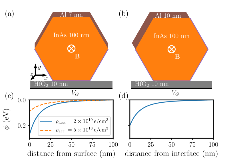
In Figs. 1 (a) and (b) we show the hexagonal cross sections of two nanowire devices covered by three and two facets of Al respectively, representing the devices experimentally investigated in Ref. Vaitiekėnas et al. (2018a). InAs is known to have a strong surface accumulation layer at the pristine InAs surface Olsson et al. (1996); Degtyarev et al. (2017). We model [0001] wurtzite InAs nanowires, for which the precise parameters of the surface accumulation layer are presently unknown. Therefore, we choose the parameters compatible with existing measurements of different surfaces. We model the accumulation layer by depositing a 1 nm layer of positive charge density on the InAs surface. We simulate results for two cases: cm-3 and cm-3.
For cm-3, the average charge density is about cm-3 in the semiconductor wire at zero gate voltage, consistent with the reported electrical characterizations of such wires Thelander et al. (2010). In the absence of other charges and gates, the conduction band of InAs is pinned about 0.25 eV below the Fermi level at the surface [see the 1D simulation in Fig. 1 (c)]. To investigate the influence of the accumulation layer we simulate also cm-3, for which the conduction band of InAs is pinned about 0.1 eV below the Fermi level at the surface consistent with different characterizations of InAs nanowires Degtyarev et al. (2017).
In the case of the InAs/Al interface, we assume a similar conduction band offset to the Fermi level of 0.2 eV, presumably resulting from the work function difference between the two materials. The presence of band bending at the semiconductor-superconductor interface has recently been identified to be a crucial ingredient for the strong proximity effect Antipov et al. (2018); Mikkelsen et al. (2018). This specific value of the conduction band offset is motivated by recent angle resolved photo-emission spectroscopy (ARPES) measurements of InAs with a thin layer of epitaxial Al Schuwalow et al. . In the electrostatic simulation the Al layer is assumed to be grounded. It enters the Poisson equation only in the form of a Dirichlet boundary condition, which is set to 0.2 V due to the work function difference to InAs [see also Fig. 1 (d)]. A backgate is located below the dielectric layer, set to the backgate voltage . On the remaining three boundaries of the system we assume Neumann conditions. For the dielectric constant of InAs and HfO2 we use the values 15.15 and 25 correspondingly Wilk et al. (2001).
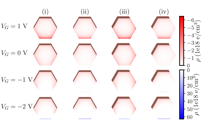
The resulting electron and hole densities are shown in Fig. 2, calculated from the self-consistent electrostatic potential and Eq. (3) and (4). We consider four different electrostatic configurations (i)-(iv), corresponding to the two different wire designs with three and two facets covered by Al and two different accumulation layers shown in Fig. 1 (c).
Based on the density plots shown in Fig. 2 we distinguish three generic cases for the localization of the electrons: For we find most electrons to be localized close to the gate. For we see the electron density forming a ring of charge at the surface of the semiconductor, resulting from the accumulation layer of InAs. At more negative voltages the only electrons left are near the InAs-Al interface.
Note that we find hole accumulation for V in configuration (i, iii) [ in configuration (ii, iv)] in Fig. 2. This is a consequence of the small distance of the backgate to the wire and of the small band gap of InAs. Due to the large effective mass of the hole states they are very effective at screening the gate once the potential becomes large enough for them to be populated. While the screening length of the electrons is on the order of 10-20 nm, the screening length of the holes is about a magnitude shorter on the scale of nm. Going to more negative gate voltage has little effect on the system since the gate is then screened by the holes.
II.2 Schrödinger solver
After the electrostatic potential is calculated for a given geometry and backgate voltage we plug it into the Schrödinger equation and solve it for the cross-section of the device. The normal-state Hamiltonian for InAs/Al heterostructure reads
| (5) | ||||
with the momentum-operator , the effective mass , the Fermi level , the electrostatic potential (possibly including a disorder potential) and the g-factor . Here are Pauli matrices acting on spin degrees of freedom. We assume the wire to be aligned parallel to the -direction and the Hamiltonian to be translation-invariant in . The vector contains the Rashba parameters and resulting from the electric field in the semiconductor, and the Dresselhaus parameter resulting from the bulk inversion asymmetry of wurtzite-InAs Lew Yan Voon et al. (1996). The material parameters for InAs and Al are summarized in Tab. 1. Note that when solving the Poisson equation we assume that Al is a perfect metal (i.e. impose the corresponding boundary conditions). Thus, is not solved for inside of Al and is set to zero there.
| Parameter | InAs | Al |
|---|---|---|
| 0.0229 Winkler et al. (2003) | ||
| 0.03 eVnm Gmitra and Fabian (2016) | 0 eVnm | |
| -14.9 Winkler et al. (2003) | 2.0 | |
| 0 meV | 0.34 meV Cochran and Mapother (1958) | |
| 0 eV | 10 eV |
We take into account superconductivity at the mean-field level. The corresponding Bogoliubov-de-Gennes (BdG) Hamiltonian in Nambu space Tinkham (1996) reads
| (6) |
Here the superconducting pairing is non-zero only in the superconductor (the superconducting phase is also only defined there).
The orbital effect is added to Eq. (6) via the minimal substitution
| (7) |
with being the vector potential. The BdG Hamiltonian Eq. (6) is gauge-invariant under transformations of the form Tinkham (1996)
| (8) | ||||
The supercurrent in the superconductor is given by
| (9) |
where is the superconducting density. Since in our simulations we always deal with very thin superconducting films, we neglect any screening effect of the superconductor and assume a homogeneous magnetic field. The vector potential and phase are chosen such that Eq. (9) leads to a physically correct distribution of , see App. A for details.
The Rashba couplings and are nonzero only in the semiconductor region and result from the symmetry breaking by the electrostatic potential Soluyanov et al. (2016). We estimate the Rashba couplings from the average electric field in the semiconductor region from 8-band k.p-theory Winkler et al. (2003)
| (10) |
where the average electric field in direction is obtained by averaging , calculated from the electrostatic potential , over the whole semiconductor region. This procedure neglects surface terms and the fact that wave functions might be localized more in the steep parts of the potential, therefore it gives a conservative, lower-bound, estimate for the Rashba spin-orbit coupling. The following parameters for bulk InAs are used in accord with Ref. Winkler et al., 2003: eV nm, eV and eV. In Fig. 3 we give the bare Rashba parameters as a function of gate voltage for the different devices.
The Hamiltonian Eq. 6 is discretized on a quadratic mesh using the kwant package Groth et al. (2014). A lattice constant of 0.1 nm is used for the discretization to accommodate the small Fermi wavelength of Al. The interior eigenvalues close to the Fermi level of the sparse Hamiltonian are calculated with the shift-invert method as implemented in SciPy Jones et al. (01), however, replacing the SuperLU algorithm packaged with SciPy with the more efficient MUMPS library Amestoy et al. (2001, 2006). With this numerical approach we are able to solve for interior eigenvalues of tight-binding Hamiltonians with several millions of basis states.
III Zero magnetic field
A hard induced superconducting gap in the semiconductor is one of the prime achievements of epitaxial InAs/Al hybrid nanowires Chang et al. (2015). In these devices typically two to three facets of the hexagonal wire are covered by a layer of Al. To achieve critical magnetic fields that are large enough to form MZMs the superconducting layer is kept very thin, between 5 to 10 nm in typical devices. While the superconducting layer is very thin it also has a very large density of states (DOS). Therefore, in a hybrid device the induced gap in the semiconductor is often found to be of the same order as the superconductor gap Krogstrup et al. (2015).
The combined results for the minimal induced gap are shown in Fig. 4. All devices have large induced gap for appropriate gate voltages. We now discuss the four different electrostatic configurations presented in Fig. 2 and the effects of disorder in detail.
III.1 Three-facet device
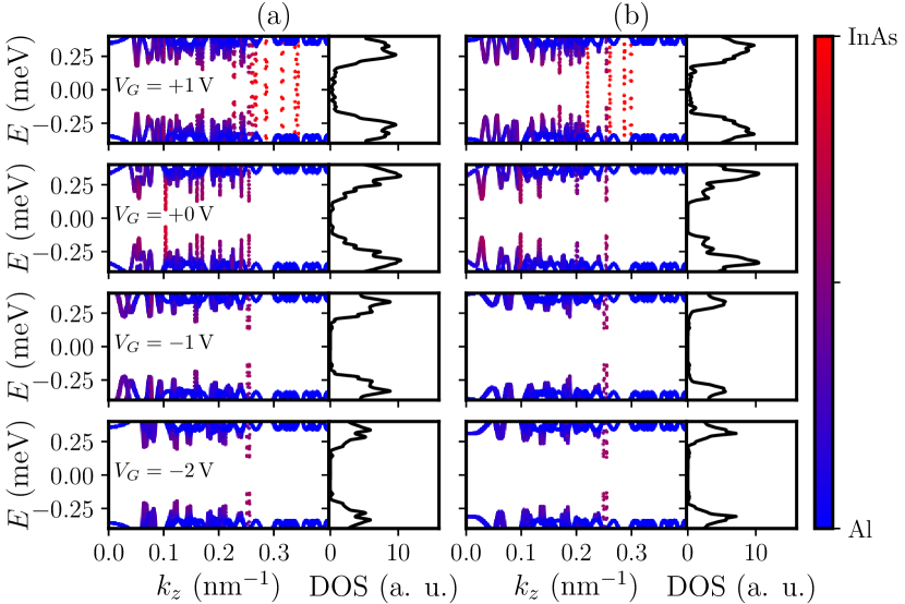
In Fig. 5 we show the energy spectrum and DOS in the InAs region for different backgate voltages in the three-facet wire. For all backgate voltages we find semiconductor-like states that have a strong hybridization with the superconductor. These states appear below the Al gap, but have a strong hybridization with Al as indicated by the color in Fig. 5. The DOS in the semiconductor is obtained by integrating the band structure over momentum, multiplying each eigenstate by its weight in the semiconductor 222We cut-off the integration at since the weight in the semiconductor is negligible for larger momenta.. A temperature broadening of the energy levels of 50 mK is assumed. The calculated DOS is consistent with experiment Chang et al. (2015); Gazibegovic et al. (2017): For negative gate voltages we typically find a hard gap, with the position of the coherence peaks showing little dependence on gate voltage. For positive gate voltages non-superconducting states enter the gap.
At positive backgate voltages, we find accumulation of electrons near the backgate, on the opposite side of Al. These states live almost completely in the InAs region and have negligible hybridization with the superconductor and thus no, or very small, induced gap. They contribute to a subgap conductance for .
Around the electron density is distributed along the surface of the semiconductor (see Fig. 2). In this regime all states have non-zero hybridization with the superconductor and a hard gap opens up.
For sufficiently negative backgate voltage the only states left are in close proximity to the superconductor. These are characterized by strong hybridization and induced gap on the order of the superconductor gap. Note that a single state at nm-1 has significantly smaller hybridization and induced gap than the other states in Fig. 5 (a) and (b) for V. Furthermore, note that our Schrödinger solver only includes the electrons, hence no hole states show up in the DOS and band structures of Fig. 5. According to Fig. 2 hole accumulation would be expected for V for Fig. 5 (a) [ V for (b)].
III.2 Effect of disorder on the induced gap
Some previous attempts at simulating the superconducting proximity effect by treating the semiconductor and superconductor on equal footing often found an induced gap that is strongly dependent on geometric and microscopic details and significantly smaller than the one reported in experiments Reeg et al. (2017); Mikkelsen et al. (2018). This is a consequence of the constraint imposed by momentum conservation at a smooth interface between semiconductor and superconductor. In such a case, tunneling between the two subsystems is suppressed due to energy and momentum constraints. Indeed, in this case tunneling rate, which is relevant for the proximity effect Stanescu et al. (2011), is effectively proportional to one-dimensional DOS and decreases with . Since is large in metals such as Aluminum, at any given parallel momentum the phase space which satisfies both constraints is small. In other words, the level spacing coming from one-dimensional sub-band quantization in the superconductor is several orders of magnitude larger than the superconducting gap for Al films with a thickness of 10 nm. This results in a strong and non-monotonic dependence of the induced gap on the thickness of the superconductor Mikkelsen et al. (2018). This dependence on the thickness of the superconductor is not observed in experiment and is an artifact of a parallel-momentum-conserving approximation at the surface. In fact, experimentally the opposite effect is observed, that the gap is enhanced for thinner Al thicknesses Douglass and Meservey (1964); Meservey and Tedrow (1971).
Ref. Antipov et al. (2018) demonstrated that disorder in the superconductor enhances the induced gap dramatically and, provided it is sufficiently strong, removes the non-monotonic dependence on the thickness of the superconducting layer. Since a fully three dimensional simulation of a semiconductor-superconductor heterostructure would be extremely challenging, the disorder potential is chosen independent of , such that the momentum parallel to the nanowire axis remains conserved. This disorder breaks the momentum conservation in one direction parallel to the interface so that the semiconductor is now hybridized by an effectively two dimensional superconductor. The level spacing resulting from two-dimensional quantization in the superconducting film is smaller than the superconducting gap in the hybrid device geometries investigated here. In reality, three-dimensional disorder in the superconductor breaks the momentum conservation also in the longitudinal direction, possibly enhancing the hybridization and the induced gap even further. Our two-dimensional disorder model is sufficient to qualitatively describe the effect of disorder on the hybridization of the semiconductor with the superconductor. However, in the topological phase a three-dimensional model of disorder will also lead to a number of new qualitative features such as impurity-induced subgap states Lutchyn et al. (2012); Cole et al. (2016); Liu et al. (2018), which is not captured by our model. We also do not consider here disorder in the semiconductor. High-quality semiconductor nanowires have been shown to be very clean with a mean free path of the order a micron Lutchyn et al. (2018). Both of these effects are outside the scope of this work.
Furthermore, we note that in our simulations the momentum conservation at the semiconductor-superconductor interface is already broken due to the non-planar (i.e. hexagonal) shape of the Al shell. We find that this has very similar effects as adding disorder to the system, i.e. we find large induced gaps that depend only weakly on the geometry and thickness of the superconducting layer.
While the semiconductor and also the interface to the superconductor is very clean Krogstrup et al. (2015), the Al is naturally covered by an amorphous oxide layer. This oxide layer provides a motivation to investigate — additionally to the non-planar interface — the effect of disorder on the surface of the Al shell. Motivated by this physical model, we restrict the disorder to a layer of 2 nm thickness from the outside of the shell. We use random on-site chemical potential in the specified region to simulate disorder. The disorder potential itself is sampled from a Gaussian distribution with a variance of 1 eV. The disorder strength and thickness are chosen such that an electron experiences on average one scattering event while being reflected at the Al-vacuum interface, corresponding to a mean-free path of the order of the thickness of the superconductor.
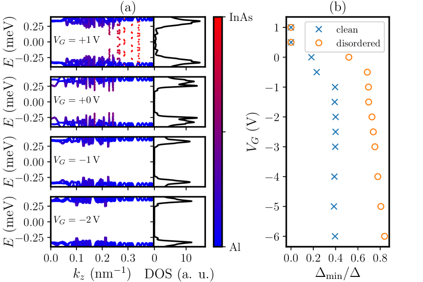
In Fig. 6 we show that disorder is able to significantly enhance the size of the induced gap. With disorder, all states close to Al show very strong hybridization and induced gap on the order of 80% of the Al gap at negative gate voltages. On the other hand, the states contributing to the subgap conductance at positive gate voltages are not affected by the presence of disorder in Al, consistent with them having no weight in the superconductor.
III.3 Two-facet device
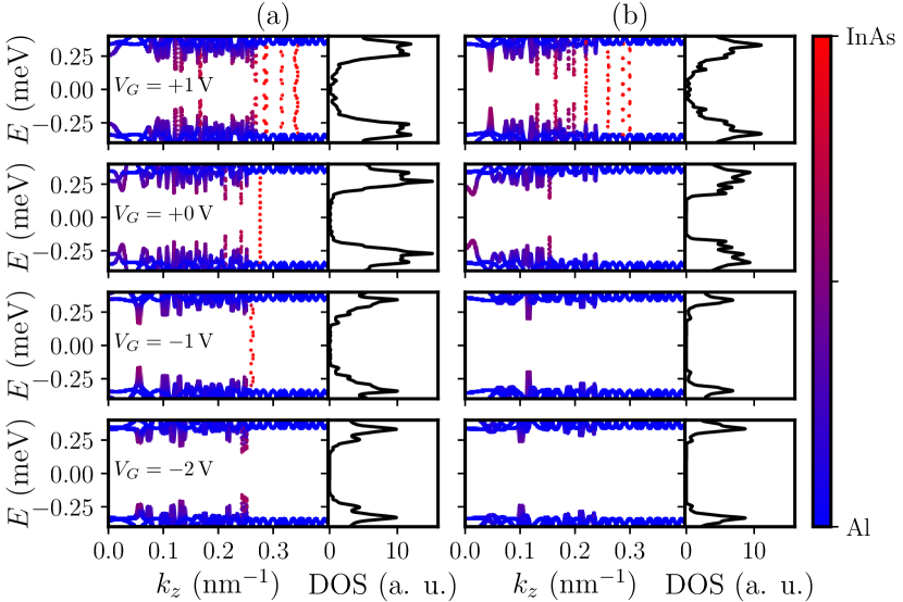
In Fig. 7 we show the electronic states and DOS in the two-facet device for different backgate voltages. In general, we find very similar results to the three-facet device.
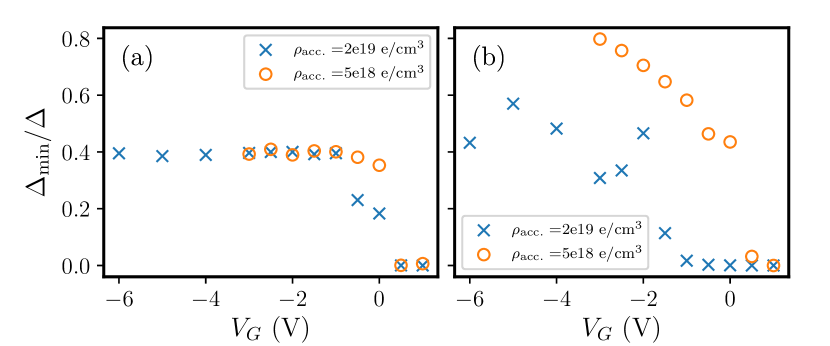
We find that the backgate voltage at which the gap becomes hard is very different for the different accumulation layers, with the threshold being V for e/cm3 and V for e/cm3. The reason for this becomes apparent when comparing the density distributions of the two cases in Fig. 2. Due to their accumulation layer hexagonal InAs nanowires have a tendency to accumulate a higher density in their corners than below their facets Degtyarev et al. (2017). In the two-facet device there is a corner that is not adjacent to the Al-shell or the backgate. The states living in this corner have no weight in the superconductor analog to the gate states and therefore result in a reduced gap compared to the three-facet device. In the strong accumulation layer case e/cm3 large negative backgate voltage V is required to open a superconducting gap for these states.
For the weak accumulation layer case ( e/cm3) one finds even enhanced induced gap compared to the three-facet device at large negative gate voltage, although, comparable to the gap of the three-facet device with disorder. The induced gap in the clean two-facet device is comparable to the three-facet device with disorder, see Fig. 4. This might be related to two effects: First, the two-facet device has less symmetry than the three-facet device, as it lacks the vertical mirror symmetry. Removing this symmetry allows a stronger hybridization of semiconductor and superconductor states. Another difference is the thickness of the superconducting layers for the two devices, which is investigated in App. C. We find that a thicker superconductor also hybridizes the semiconductor more strongly.
IV Finite magnetic field
Upon turning on a magnetic field parallel to the wire, and for appropriate gate voltages, the system can transition into the topological phase supporting MZMs Lutchyn et al. (2010); Oreg et al. (2010). It is desirable for the critical field of the topological transition to be as small as possible, and in particular to be much lower than the critical field of the superconducting (e.g. Al) shell. In this section, we first investigate the bulk DOS as a function of magnetic field and the behavior of as a function of gate voltage, which is important to determine the magnitude of the critical field of the topological transition. Then, we investigate the topological phase diagram.
IV.1 Density of states

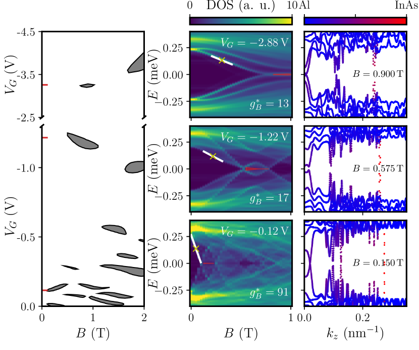
Transport experiments in Majorana nanowires measuring the differential conductance can be related to the local DOS at the tunnel contact if the tunneling rate is small Datta (1997). In our simulations we calculate the DOS in the middle of an infinite wire. Therefore, no MZMs are visible with the only sign of the topological phase transition being the bulk gap closing. Furthermore, we expect that the experimentally obtained differential conductance will show bulk states with different relative intensity than in bulk DOS simulations Datta (1997).
In Fig. 8 we show the bulk DOS as a function of magnetic field and energy for six different backgate voltages. Both cases, where the system undergoes a topological phase transition and where it stays trivial in the range of magnetic fields, are presented. In the topological cases we indicate the topological gap in red. Due to the very large size of the Hamiltonian matrix it is impossible to directly evaluate the Pfaffian to determine the topological phase Kitaev (2001). Instead, we use the fact that the gap of the Hamiltonian at closes, always and only at topological phase transitions. Considering further that the system must be in the topologically trivial phase for , one can determine the location of the topological phase this way.
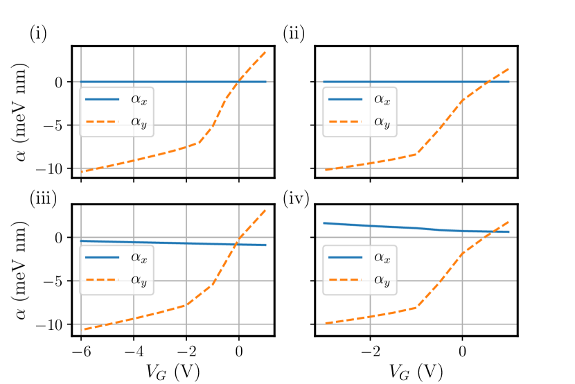
Regardless of topological character, we define similar to the experiment Ref. Vaitiekėnas et al. (2018a) as the slope of the lowest-energy states represented in the DOS. For the cases in Fig. 8, in which the system undergoes a topological phase transition, the gap closes linearly with and is independent of at which it is extracted. In the non-topological cases, however, the interplay of spin-orbit coupling and finite chemical potential typically lead to a nonlinear gap dependence with 333In the non-topological cases the gap becomes extremely small, but does not close in general.. In these cases we choose the magnetic field such that is maximized.
We observe a clear trend in the dependence of on the backgate voltage, see Fig. 9. In Fig. 9 (a) we show results for without the orbital effect of magnetic field. Since is directly affected by the renormalization of the -factor, it is an indicator of the coupling strength of semiconductor to superconductor. In general, we find a non-monotonic behavior, resulting from the different coupling strengths of the different subbands, although showing already a trend in , with large values of only at positive or small negative backgate voltages. The trend becomes even more pronounced in Fig. 9 (b) where the orbital effect of magnetic field is included. This is a result of the orbital effect being very sensitive to the extent of the wavefunction, which is tuned by the backgate. For positive, or small negative, backgate voltages the slope is significantly larger than the bulk -factor of InAs, corresponding to an orbital enhancement of -factor as discussed in Ref. Winkler et al. (2017). At this gate voltages states are localized in the accumulation layer, along the surface of InAs. These states are strongly influenced by the orbital effect since they are easily penetrated by magnetic flux. For large negative gate voltages, however, the wave functions are confined close to the superconductor, and the orbital effect is suppressed.
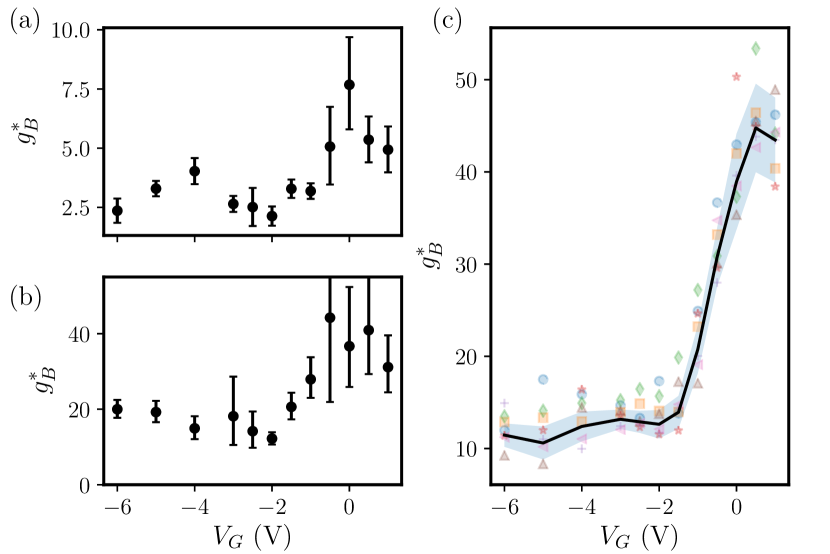
In Fig. 9 (c) we investigate the effect of disorder, for the same system as in Fig. 6. We find that while is more dependent on the disorder realization than the induced gap, the typical variation is often still less than the error bar of our fit. The main effect of disorder is that it further enhances the coupling of semiconductor with superconductor, resulting in effective g-factors smaller than in the case without disorder. Also the step-like behavior of with backgate voltage becomes more pronounced, being very close to the one measured in experiments Vaitiekėnas et al. (2018a). Still, even after taking disorder into account we find that our values of are often overestimated compared to the experiment. This might be a limitation of our Hamiltonian Eq. (6), which does not include confinement effects on the InAs -factor and the effective mass Stein et al. (1983); Lommer et al. (1985); Ivchenko and Kiselev (1992). Implementing a more sophisticated Hamiltonian, like the 8-band Kane Hamiltonian Kane (1957), might be required for more accurate results, although it would be very difficult due to the prohibitive computational cost resulting from the very dense discretization.
IV.2 Magnetic interference effects
Because of the accumulation layer and the electrostatic screening the system obtains a ring-like charge density for positive backgate voltage, see Fig. 10 (a) which is a special case of Fig. 2. In this configuration the system is very susceptible to orbital effects, resulting as we have seen in strongly enhanced . Furthermore, we find that, in this regime, the DOS shows an oscillatory behavior with magnetic field following the first bulk gap closing, see Fig. 10 (b). The minima correspond roughly to a magnetic field in which half-integer magnetic flux quanta penetrate the cross section of the wire. The maxima correspond roughly to integer flux quanta.
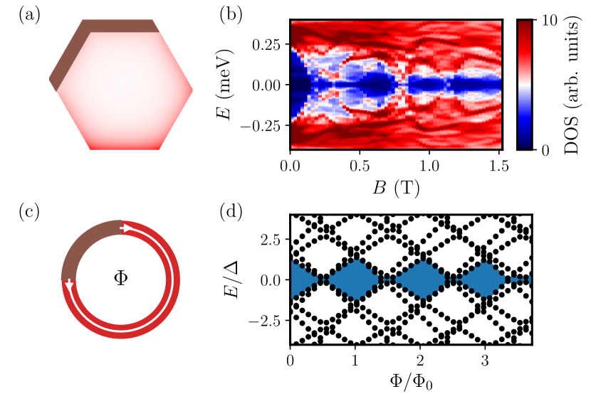
The basic mechanism of the oscillating induced gap can be understood in a crude toy model depicted in Fig. 10 (c). For simplicity, it is assumed that the superconducting segment (shown in brown) is longer than the coherence length. Then one can view the semiconducting segment as a Josephson junction, in which the Andreev bound states depend on the phase controlled by the magnetic flux penetrating the ring 444Note that similar toy models have been investigated in Ref. Büttiker and Klapwijk (1986); Sticlet et al. (2017), although the geometry was not motivated by the electrostatics there.. The resulting spectrum is plotted in Fig. 10 (d). The minima correspond to values of flux in which this phase is a half-integer multiple of , the maxima to integer multiple of . In this toy model, the wave functions are all sensitive to the same magnetic flux, leading to very regular oscillations of the energy gap. On the other hand, in the realistic simulations different wave function can have a different effective area, and thus the oscillations are much less regular. In particular, after the first bulk gap closing in Fig. 10b, the bulk energy gap never quite recovers to the initial value. For details about the toy model calculation see App. B.
IV.3 Phase diagram
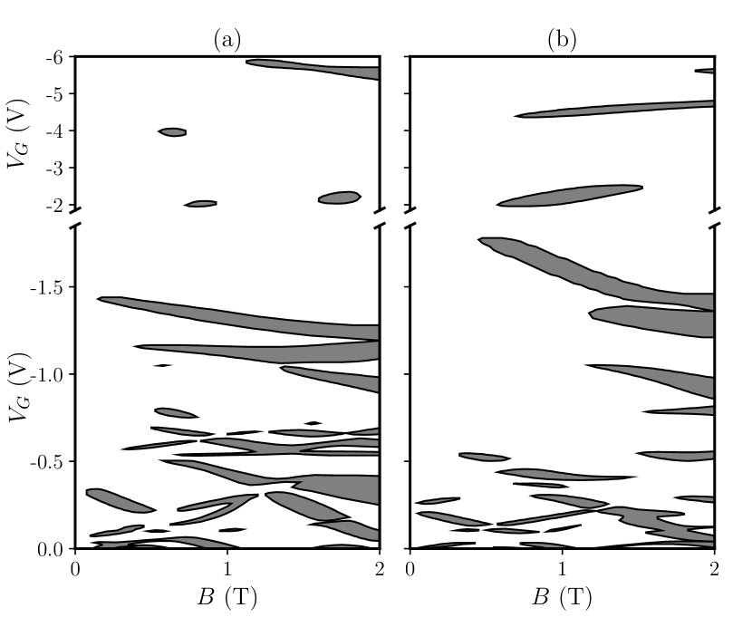
Now we study the topological phase diagram in the presence of electrostatic, orbital and renormalization effects. Early attempts of calculating the topological phase diagram of Majorana nanowires typically did not include electrostatics effects, but show the phase boundaries as a function of the chemical potential rather than the gate voltage Lutchyn et al. (2010); Oreg et al. (2010); Tewari et al. (2012); Stanescu et al. (2011); Nijholt and Akhmerov (2016). Only recently phase diagrams as a function of a gate voltage have been obtained Vuik et al. (2016); Antipov et al. (2018). The orbital effect on the phase diagram has been studied in Ref. Nijholt and Akhmerov (2016), although without including electrostatic effects. In this section, we consider clean semiconductor-superconductor heterostructure, i.e. no disorder.
In Fig. 11 (a) we show the phase diagram of the three-facet device without orbital effects. The phase diagram looks similar to earlier findings of multi-subband wires Tewari et al. (2012); Stanescu et al. (2011); Antipov et al. (2018), although we find a strong dependence of the semiconductor-superconductor coupling on the subband, resulting in a large variation of minimal critical magnetic fields corresponding to the phase transition. As has also been pointed out in Ref. Antipov et al. (2018), the lever arm of chemical potential vs gate voltage is significantly larger at positive or small negative gate voltages than at large negative ones. Consequently, the density of topological phases is higher in for small negative gate voltages in Fig. 11. The reason for this is twofold: first, the electron states localized near the gate are more easily tuned by the backgate than the states close to the superconductor. Second, the screening effect of the holes decreases the lever arm further for large negative gate voltage. In general, not taking orbital effect into account leads often to magnetic fields, at which the topological phase transitions, being large compared to experiments.
Turning the orbital effect on in Fig. 11 (b) changes the shapes of the phase boundaries dramatically. For small negative gate voltages the phase diagram is dominated by the orbital effect of magnetic field. This becomes apparent due to the small magnetic fields at which the topological transition occur and the very non-parabolic shape of the phase boundaries. In this regime one often finds two topological regions emerging close in gate voltage at similar magnetic fields, that separate from each other, one drifting to larger gate voltages and the other to smaller gate voltages. These result from two subbands that are near angular momentum eigenstates, with approximately opposite angular momentum Winkler et al. (2017). One of the reasons why the orbital effect is so strong is the high electron density, which is a result of the large band-offset of InAs/Al and the accumulation layer resulting in about ten occupied subbands in InAs. High subbands have high orbital quantum numbers coupling strongly to magnetic field Winkler et al. (2017). At large negative gate voltage the orbital effect is suppressed and the phase boundaries look closer to the ones without orbital effect, although the influence of the orbital effect is still strongly present.
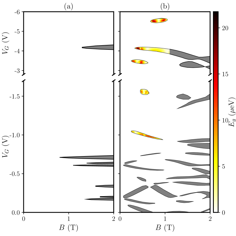
From Fig. 11 (b) it becomes apparent that only topological phases with appreciable negative backgate voltage have a sizable topological gap. We find that the maximum topological gap is only slightly larger than 20 eV. While this seems like a small value we emphasize that it is proportional to the strength of the Rashba spin-orbit coupling. In our calculation, the value of spin-orbit coupling is conservatively since we take only electrostatic origin of spin-orbit coupling int account. The value of we obtain from Eq. (10) is typically about 10 meVnm, whereas experiments report values in the range of 10 to 30 meVnm Roulleau et al. (2010); Liang and Gao (2012) which would result in a significantly larger topological gap.
IV.4 Effect of broken mirror symmetry in the two-facet device
In terms of symmetries, the most significant difference between the three- and two-facet devices is the vertical mirror symmetry in the -plane . Additionally considering the particle-hole symmetry , , which protects the MZMs, and the time-reversal symmetry , it can be shown that the combination of the three symmetries create a chiral symmetry
| (11) |
that survives at finite magnetic field parallel to the mirror plane. For the specific case of our Hamiltonian Eq. (6) the chiral symmetry is given by (with being the real-space reflection operator taking to ). Note that the Rashba term breaks this chiral symmetry.
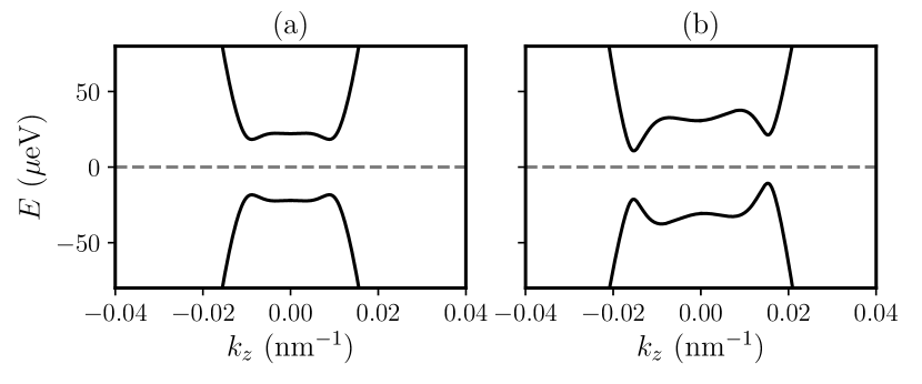
One particular consequence of the chiral and particle-hole symmetry is that the band structure is line-reflection symmetric around the and axes, see Fig. 12 (a). In the two-facet device the chiral symmetry is broken because of the missing mirror symmetry . Therefore, the band structure is only point-inversion symmetric around the point, as dictated by the particle-hole symmetry. At finite this generically leads to a tilting of the band structure that is detrimental to the topological gap, as is shown in Fig. 12 (b). At the time-reversal symmetry prevents any tilting of the band structure, see Fig. 7. It has been pointed out in Ref. Nijholt and Akhmerov (2016) that a possible mirror perpendicular to the wire axis would also prevent any tilting of the band structure. The wurtzite Dresselhaus term breaks this mirror symmetry in our case. Note that in [111] zincblende wires the Dresselhaus term is expected to be much smaller, due to the fact that it is cubic in as opposed to linear in in the wurtzite case Dresselhaus (1955); Gmitra and Fabian (2016). Therefore, it is expected that the tilting effect of the band structure is significantly smaller in non-mirror-symmetric [111] zincblende wires than in non-mirror-symmetric [0001] wurtzite wires, although it would still be present.
V Summary and Conclusions
In this work, we presented a unified numerical approach for realistic simulation of semiconductor-superconductor heterostructures which adequately treats all the important effects in these systems: proximity-induced superconductivity, orbital and Zeeman effect of an applied magnetic field, disorder, spin-orbit coupling as well as electrostatic environment and realistic geometry (hexagonal cross-section). We considered InAs/Al hybrid nanowires as a model system and compared our numerical results with the existing experimental data. We calculated topological phase diagrams for InAs/Al hybrid nanowires and quasiparticle gaps in corresponding topological phases which is important data for the topological qubit design proposals and can be used to optimize the designs for Majorana-based qubits. Furthermore, the approach developed here can be readily extended to other topological semiconductor-superconductor platforms such as 2DEG platforms Shabani et al. (2016); Nichele et al. (2017); Suominen et al. (2017), quasi-one-dimensional networks obtained by selective area growth Vaitiekėnas et al. (2018b); Krizek et al. (2018) or nanowires with a full superconducting shell Vaitiekėnas et al. (2018); Lutchyn et al. (2018).
We first investigated the dependence of the subgap density of states on the gate voltage at zero magnetic field. We identified states that live near the gate (i.e. opposite to the interface with Al) and within the accumulation layer of the pristine InAs surface to be responsible for a subgap density of states for positive gate voltages. We find that at moderate negative gate voltages the dominant contribution to the subgap density of states comes from the states localized close to the InAs/Al interface which are very strongly proximitized, resulting in a large proximity-induced gap and hard gap in the semiconductor. We also considered the effect of disorder in the superconducting shell and found that it increases the semiconductor-superconductor coupling, leading to an enhanced induced gap.
Next, we investigated the dependence of the energy spectrum on external magnetic field and studied the evolution of the spectrum as a function of electric and magnetic fields. In particular, we calculated the effective -factor for subgap states and showed that it has a non-monotonic dependence on gate voltage, consistent with the experimental data Vaitiekėnas et al. (2018a). This non-monotonic dependence appears due to the interplay of two competing effects: renormalization of the effective model parameters in the strong tunneling regime and orbital contribution to . Therefore, even in the strongly proximitized regime, the InAs/Al hybrid device is able to support MZMs at moderate magnetic fields.
We characterized topological superconductivity in hybrid InAs/Al nanowires by calculating topological phase diagram as well as the corresponding topological excitation gaps. Given that magnetic fields of topological phase transitions in hybrid InAs/Al nanowires are significantly smaller than expected from a simulation including only the Zeeman term, we show that inclusion of the orbital effect is crucial for a quantitative and qualitative understanding of the topological superconductivity in proximitized nanowires.
We also investigated the microscopic origin of the spin-orbit coupling in proximitized nanowires. We found that the interplay of Dresselhaus term (resulting from the wurtzite structure) and broken mirror symmetry lead to a tilt of the band structure in the two-facet device, which is absent in mirror-symmetric three-facet devices. Therefore, we recommend using wires with symmetrical Al shells and gate congurations for Majorana applications, particularly in the case of wurtzite wires.
Finally, we emphasize that the level of detail of our modeling sets a new standard for simulations of hybrid semiconductor-superconductor nanowires, that should be also applied to different Majorana platforms employing semiconductor-superconductor heterostructures. One of the remaining challenges is a fully three dimensional simulation of a hybrid device including scattering and disorder in the superconductor. Indeed, although our two dimensional disorder model is sufficient to capture correctly some properties of the hybrid system like the magnitude of the induced gap at zero magnetic field, it is not adequate for understanding the impact of longitudinal disorder on the topological phase in the limit of strong coupling between the semiconductor and the superconductor.
Acknowledgements.
We acknowledge stimulating discussions with Anton Akhmerov, Bogdan A. Bernevig, Ming-Tang Deng, Karsten Flensberg, John Gamble, Jan Gukelberger, Panagiotis Kotetes, Peter Krogstrup, Charlie Marcus, Michiel de Moor, Bas Nijholt, Enrico Rossi, Jie Shen, Saulius Vaitiekėnas and Hao Zhang. L.I.G. acknowledges the support of NSF DMR Grant No. 1603243. A.A.S. acknowledges the support of SNSF through NCCR MARVEL and QSIT grants, the SNSF Professorship and Microsoft Research. This work was performed in part at Aspen Center for Physics, which is supported by National Science Foundation grant PHY-1607611.Appendix A Supercurrent distribution
If both superconductivity and orbital effect of magnetic field are considered in the same system, it is crucial that the combination of vector potential and superconducting phase results in correct physical observables. Due to the much higher density of electrons in the superconductor compared to the semiconductor we consider the superconductor film for these considerations to be independent of the semiconductor. In this case, and at zero temperature, the superconductor will minimize its kinetic energy which is proportional to Tinkham (1996). The correct vector potential and phase can be obtained by minimizing this expression Wójcik and Nowak (2018). Since the London penetration depth of Al is much larger than the thickness of the Al film we neglect screening effects of the supercurrent. For the simple geometry at hand we are able to write down an analytical solution for the vector potential and superconducting phase which approximates the full solution.
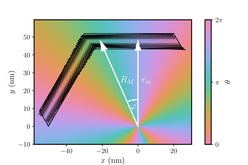
We take the vector potential in the cylindrical gauge
| (12) |
Furthermore, we choose the phase such that the supercurrent Eq. (9) is canceled exactly in the middle of the superconducting film. This is achieved by satisfying , with corresponding to the radius to the middle of the superconducting film, see Fig. 13. Due to the hexagonal shape of the film is a function of : for (see Fig. 13 for the definition of ). Therefore, the phase is given by
| (13) |
for .
In Fig. 13 we show the resulting supercurrent distribution and phase (we continue to plot the face outside of the superconductor, even though it is strictly speaking not defined there). Since the supercurrent takes only small values the kinetic energy of the superconductor is close to the minimum value and also the boundary conditions are fulfilled with this choice in a good approximation. Furthermore, we find that our results are not strongly dependent on the exact choice of vector potential and phase dependence as long as the kinetic energy is close to the minimal value. If the magnetic flux through the hexagon of size is not an integer multiple of the magnetic flux quantum the superconducting phase needs to have a discontinuity somewhere. Since in none of our geometries all facets are covered by the superconductor this jump can be conveniently located along a line that does not go through a superconducting region.
Appendix B Toy model
For the toy model calculation we assume a simple BdG Hamiltonian without spin-orbit coupling or Zeeman
| (14) |
where we use , eV and eV. The vector potential is added via the substitution Eq. (7). For the gauge and superconducting phase we proceed as described in App. A. For the inner radius of the ring we take 30 nm and for the outer radius 40 nm.
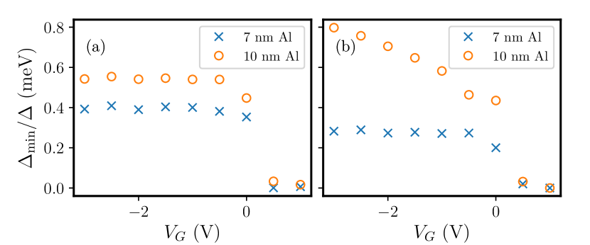
Appendix C Dependence of the induced gap on Al-layer thickness
In Fig. 14 we show the induced gaps of the two-facet and three-facet device for two different thicknesses of the Al-layer: 7 nm and 10 nm. For the thicker Al-layer the induced gap is always larger, indicating that the semiconductor-superconductor coupling is stronger in this case. Therefore, the thickness of the superconductor-layer might be used as an additional knob, in addition to the gate Antipov et al. (2018); de Moor et al. (2018), to control the strength of the semiconductor-superconductor coupling.
Appendix D Additional phase diagrams
Here we show additional phase diagrams calculated for other geometries and different accumulation layer strengths as in the main text.
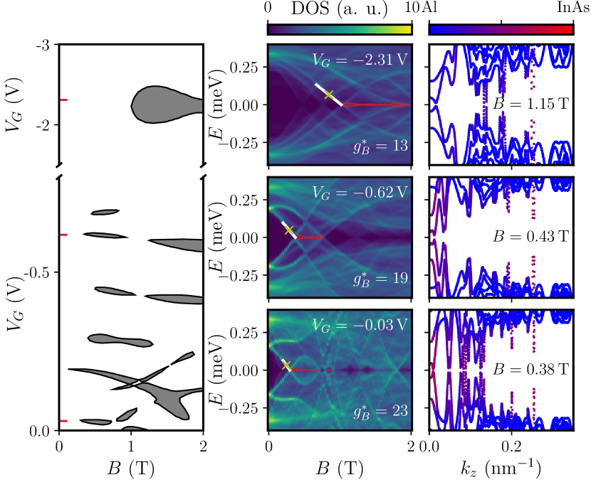
In Fig. 15 we show the phase diagram for the two-facet wire. Since calculation of the topological gap is very expensive, we show the DOS at three cuts of different topological phases at fixed gate voltage. We find that the topological phase space is greatly reduced in comparison to the three-facet device shown in Fig. 11 (b). Partly this is also caused by the thicker Al layer which is 10 nm compared to 7 nm. The effect of Al-layer thickness is further investigated in Fig. 16, where we show three-facet phase diagram for 10 nm Al thickness and a two-facet phase diagram for 7 nm Al thickness. We find that the topological phase space for the two-facet device with 7 nm Al thickness is significantly larger than with 10 nm Al thickness.
References
- Kitaev (2001) A. Y. Kitaev, Physics-Uspekhi 44, 131 (2001).
- Moore and Read (1991) G. Moore and N. Read, Nuclear Physics B 360, 362 (1991).
- Nayak and Wilczek (1996) C. Nayak and F. Wilczek, Nuclear Physics B 479, 529 (1996).
- Read and Green (2000) N. Read and D. Green, Phys. Rev. B 61, 10267 (2000).
- Ivanov (2001) D. A. Ivanov, Phys. Rev. Lett. 86, 268 (2001).
- Sau et al. (2010) J. D. Sau, R. M. Lutchyn, S. Tewari, and S. Das Sarma, Phys. Rev. Lett. 104, 040502 (2010).
- Alicea (2010) J. Alicea, Phys. Rev. B 81, 125318 (2010).
- Lutchyn et al. (2010) R. M. Lutchyn, J. D. Sau, and S. Das Sarma, Phys. Rev. Lett. 105, 077001 (2010).
- Oreg et al. (2010) Y. Oreg, G. Refael, and F. von Oppen, Phys. Rev. Lett. 105, 177002 (2010).
- Nayak et al. (2008) C. Nayak, S. H. Simon, A. Stern, M. Freedman, and S. Das Sarma, Reviews of Modern Physics 80, 1083 (2008).
- Alicea (2012) J. Alicea, Rep. Prog. Phys. 75, 076501 (2012).
- Beenakker (2013) C. Beenakker, Annu. Rev. Condens. Matter Phys. 4, 113 (2013).
- Leijnse and Flensberg (2012) M. Leijnse and K. Flensberg, Semiconductor Science Technology 27, 124003 (2012).
- Das Sarma et al. (2015) S. Das Sarma, M. Freedman, and C. Nayak, NPJ Quant. Inf. 1, 15001 (2015).
- Lutchyn et al. (2018) R. M. Lutchyn, E. P. a. M. Bakkers, L. P. Kouwenhoven, P. Krogstrup, C. M. Marcus, and Y. Oreg, Nat. Rev. Mater. 3, 52 (2018).
- Aguado (2017) R. Aguado, Riv. Nuovo Cimento 40, 523 (2017).
- Krogstrup et al. (2015) P. Krogstrup, N. L. B. Ziino, W. Chang, S. M. Albrecht, M. H. Madsen, E. Johnson, J. Nygård, C. M. Marcus, and T. S. Jespersen, Nature Mater. 14, 400 (2015).
- Chang et al. (2015) W. Chang, S. M. Albrecht, T. S. Jespersen, F. Kuemmeth, P. Krogstrup, J. Nygård, and C. M. Marcus, Nat Nano 10, 232 (2015).
- Deng et al. (2016) M. T. Deng, S. Vaitiekenas, E. B. Hansen, J. Danon, M. Leijnse, K. Flensberg, J. Nygård, P. Krogstrup, and C. M. Marcus, Science 354, 1557 (2016).
- Nichele et al. (2017) F. Nichele, A. C. C. Drachmann, A. M. Whiticar, E. C. T. O’Farrell, H. J. Suominen, A. Fornieri, T. Wang, G. C. Gardner, C. Thomas, A. T. Hatke, P. Krogstrup, M. J. Manfra, K. Flensberg, and C. M. Marcus, Phys. Rev. Lett. 119, 136803 (2017).
- Zhang et al. (2018) H. Zhang, C.-X. Liu, S. Gazibegovic, D. Xu, J. A. Logan, G. Wang, N. van Loo, J. D. S. Bommer, M. W. A. de Moor, D. Car, R. L. M. Op het Veld, P. J. van Veldhoven, S. Koelling, M. A. Verheijen, M. Pendharkar, D. J. Pennachio, B. Shojaei, J. S. Lee, C. J. Palmstrøm, E. P. A. M. Bakkers, S. D. Sarma, and L. P. Kouwenhoven, Nature 556, 74 (2018).
- Vaitiekėnas et al. (2018a) S. Vaitiekėnas, M.-T. Deng, J. Nygård, P. Krogstrup, and C. M. Marcus, Phys. Rev. Lett. 121, 037703 (2018a).
- Stanescu et al. (2011) T. D. Stanescu, R. M. Lutchyn, and S. Das Sarma, Phys. Rev. B 84, 144522 (2011).
- Cole et al. (2015) W. S. Cole, S. Das Sarma, and T. D. Stanescu, Phys. Rev. B 92, 174511 (2015).
- Sticlet et al. (2017) D. Sticlet, B. Nijholt, and A. Akhmerov, Phys. Rev. B 95, 115421 (2017).
- Antipov et al. (2018) A. E. Antipov, A. Bargerbos, G. W. Winkler, B. Bauer, E. Rossi, and R. M. Lutchyn, Phys. Rev. X 8, 031041 (2018).
- Mikkelsen et al. (2018) A. E. G. Mikkelsen, P. Kotetes, P. Krogstrup, and K. Flensberg, Phys. Rev. X 8, 031040 (2018).
- Reeg et al. (2018) C. Reeg, D. Loss, and J. Klinovaja, Phys. Rev. B 97, 165425 (2018).
- Prada et al. (2012) E. Prada, P. San-Jose, and R. Aguado, Phys. Rev. B 86, 180503 (2012).
- Rainis et al. (2013) D. Rainis, L. Trifunovic, J. Klinovaja, and D. Loss, Phys. Rev. B 87, 24515 (2013).
- Nijholt and Akhmerov (2016) B. Nijholt and A. R. Akhmerov, Phys. Rev. B 93, 235434 (2016).
- Reeg et al. (2017) C. Reeg, D. Loss, and J. Klinovaja, Phys. Rev. B 96, 125426 (2017).
- Dmytruk et al. (2018) O. Dmytruk, D. Chevallier, D. Loss, and J. Klinovaja, Phys. Rev. B 98, 165403 (2018).
- Vuik et al. (2016) A. Vuik, D. Eeltink, A. R. Akhmerov, and M. Wimmer, New Journal of Physics 18, 033013 (2016).
- Woods et al. (2018) B. D. Woods, T. D. Stanescu, and S. Das Sarma, Phys. Rev. B 98, 035428 (2018).
- Domínguez et al. (2017) F. Domínguez, J. Cayao, P. San-Jose, R. Aguado, A. L. Yeyati, and E. Prada, npj Quantum Materials 2, 13 (2017).
- Escribano et al. (2018) S. D. Escribano, A. L. Yeyati, and E. Prada, Beilstein J. Nanotechnol. 9, 2171 (2018).
- Winkler et al. (2017) G. W. Winkler, D. Varjas, R. Skolasinski, A. A. Soluyanov, M. Troyer, and M. Wimmer, Phys. Rev. Lett. 119, 037701 (2017).
- Mourik et al. (2012) V. Mourik, K. Zuo, S. M. Frolov, S. R. Plissard, E. P. A. M. Bakkers, and L. P. Kouwenhoven, Science 336, 1003 (2012).
- Rokhinson et al. (2012) L. P. Rokhinson, X. Liu, and J. K. Furdyna, Nat. Phys. 8, 795 (2012).
- Deng et al. (2012) M. T. Deng, C. L. Yu, G. Y. Huang, M. Larsson, P. Caroff, and H. Q. Xu, Nano Letters 12, 6414 (2012).
- Churchill et al. (2013) H. O. H. Churchill, V. Fatemi, K. Grove-Rasmussen, M. T. Deng, P. Caroff, H. Q. Xu, and C. M. Marcus, Phys. Rev. B 87, 241401 (2013), arXiv:1303.2407 .
- Das et al. (2012) A. Das, Y. Ronen, Y. Most, Y. Oreg, M. Heiblum, and H. Shtrikman, Nat Phys 8, 887 (2012).
- Finck et al. (2013) A. D. K. Finck, D. J. Van Harlingen, P. K. Mohseni, K. Jung, and X. Li, Phys. Rev. Lett. 110, 126406 (2013).
- Albrecht et al. (2016) S. M. Albrecht, A. P. Higginbotham, M. Madsen, F. Kuemmeth, T. S. Jespersen, J. Nygård, P. Krogstrup, and C. M. Marcus, Nature 531, 206 (2016).
- Gül et al. (2018) Ö. Gül, H. Zhang, J. D. S. Bommer, M. W. A. de Moor, D. Car, S. R. Plissard, E. P. A. M. Bakkers, A. Geresdi, K. Watanabe, T. Taniguchi, and L. P. Kouwenhoven, Nature Nanotechnology 13, 192 (2018).
- Chen et al. (2017) J. Chen, P. Yu, J. Stenger, M. Hocevar, D. Car, S. R. Plissard, E. P. A. M. Bakkers, T. D. Stanescu, and S. M. Frolov, Science Advances 3, e1701476 (2017).
- Suominen et al. (2017) H. J. Suominen, M. Kjaergaard, A. R. Hamilton, J. Shabani, C. J. Palmstrøm, C. M. Marcus, and F. Nichele, Phys. Rev. Lett. 119, 176805 (2017).
- Gazibegovic et al. (2017) S. Gazibegovic, D. Car, H. Zhang, S. C. Balk, J. A. Logan, M. W. A. de Moor, M. C. Cassidy, R. Schmits, D. Xu, G. Wang, P. Krogstrup, R. L. M. Op het Veld, K. Zuo, Y. Vos, J. Shen, D. Bouman, B. Shojaei, D. Pennachio, J. S. Lee, P. J. van Veldhoven, S. Koelling, M. A. Verheijen, L. P. Kouwenhoven, C. J. Palmstrøm, and E. P. A. M. Bakkers, Nature 548, 434 (2017).
- Zhang et al. (2017) H. Zhang, Ö. Gül, S. Conesa-Boj, M. Nowak, M. Wimmer, K. Zuo, V. Mourik, F. K. de Vries, J. van Veen, M. W. A. de Moor, J. D. S. Bommer, D. van Woerkom, D. Car, S. Plissard, E. P.A.M. Bakkers, M. Quintero-Pérez, M. C. Cassidy, S. Koelling, S. Goswami, and L. P. Kouwenhoven, Nature Communications 8, 16025 (2017).
- Sestoft et al. (2018) J. E. Sestoft, T. Kanne, A. N. Gejl, M. von Soosten, J. S. Yodh, D. Sherman, B. Tarasinski, M. Wimmer, E. Johnson, M. Deng, J. Nygård, T. S. Jespersen, C. M. Marcus, and P. Krogstrup, Phys. Rev. Materials 2, 044202 (2018).
- Deng et al. (2018) M.-T. Deng, S. Vaitiekėnas, E. Prada, P. San-Jose, J. Nygård, P. Krogstrup, R. Aguado, and C. M. Marcus, Phys. Rev. B 98, 085125 (2018).
- Laroche et al. (2019) D. Laroche, D. Bouman, D. J. van Woerkom, A. Proutski, C. Murthy, D. I. Pikulin, C. Nayak, R. J. J. van Gulik, J. Nygård, P. Krogstrup, L. P. Kouwenhoven, and A. Geresdi, Nature Communications 10, 245 (2019).
- de Moor et al. (2018) M. W. A. de Moor, J. D. S. Bommer, D. Xu, G. W. Winkler, A. E. Antipov, A. Bargerbos, G. Wang, N. van Loo, R. L. M. O. het Veld, S. Gazibegovic, D. Car, J. A. Logan, M. Pendharkar, J. S. Lee, E. P. A. M. Bakkers, C. J. Palmstrøm, R. M. Lutchyn, L. P. Kouwenhoven, and H. Zhang, New Journal of Physics 20, 103049 (2018).
- Shen et al. (2018) J. Shen, S. Heedt, F. Borsoi, B. van Heck, S. Gazibegovic, R. L. M. Op het Veld, D. Car, J. A. Logan, M. Pendharkar, S. J. J. Ramakers, G. Wang, D. Xu, D. Bouman, A. Geresdi, C. J. Palmstrøm, E. P. A. M. Bakkers, and L. P. Kouwenhoven, Nature Communications 9, 4801 (2018).
- Note (1) Note that the definition of the effective “-factor” is different from the conventional definition since the slope is measured at finite magnetic field as opposed to infinitesimal magnetic field as required for defining a conventional -factor. If dependence of is linear, the two quantities coincide.
- Winkler et al. (2003) R. Winkler, S. Papadakis, E. De Poortere, and M. Shayegan, Spin-Orbit Coupling in Two-Dimensional Electron and Hole Systems, Vol. 41 (Springer, Berlin Heidelberg, 2003).
- van Weperen et al. (2015) I. van Weperen, B. Tarasinski, D. Eeltink, V. S. Pribiag, S. R. Plissard, E. P. A. M. Bakkers, L. P. Kouwenhoven, and M. Wimmer, Phys. Rev. B 91, 201413 (2015).
- Shabani et al. (2016) J. Shabani, M. Kjaergaard, H. J. Suominen, Y. Kim, F. Nichele, K. Pakrouski, T. Stankevic, R. M. Lutchyn, P. Krogstrup, R. Feidenhans’l, S. Kraemer, C. Nayak, M. Troyer, C. M. Marcus, and C. J. Palmstrøm, Phys. Rev. B 93, 155402 (2016), arXiv:1511.01127 .
- Wójcik and Nowak (2018) P. Wójcik and M. P. Nowak, Phys. Rev. B 97, 235445 (2018).
- Olsson et al. (1996) L. O. Olsson, C. B. M. Andersson, M. C. Håkansson, J. Kanski, L. Ilver, and U. O. Karlsson, Phys. Rev. Lett. 76, 3626 (1996).
- Degtyarev et al. (2017) V. E. Degtyarev, S. V. Khazanova, and N. V. Demarina, Scientific Reports 7, 3411 (2017).
- Kittel and Hunklinger (2013) C. Kittel and S. Hunklinger, Einführung in die Festkörperphysik, Einführung in die Festkörperphysik (Oldenbourg Wissenschaftsverlag, Munich, 2013).
- Thelander et al. (2010) C. Thelander, K. A. Dick, M. T. Borgström, L. E. Fröberg, P. Caroff, H. A. Nilsson, and L. Samuelson, Nanotechnology 21, 205703 (2010).
- (65) S. Schuwalow, N. Schröter, J. Gukelberger, and P. Krogstrup, To be published.
- Wilk et al. (2001) G. D. Wilk, R. M. Wallace, and J. M. Anthony, Journal of Applied Physics 89, 5243 (2001).
- Lew Yan Voon et al. (1996) L. C. Lew Yan Voon, M. Willatzen, M. Cardona, and N. E. Christensen, Phys. Rev. B 53, 10703 (1996).
- Gmitra and Fabian (2016) M. Gmitra and J. Fabian, Phys. Rev. B 94, 165202 (2016).
- Cochran and Mapother (1958) J. F. Cochran and D. E. Mapother, Phys. Rev. 111, 132 (1958).
- Tinkham (1996) M. Tinkham, Introduction to Superconductivity, Dover Books on Physics Series (Dover Publications, Mineola, New York, 1996).
- Soluyanov et al. (2016) A. A. Soluyanov, D. Gresch, M. Troyer, R. M. Lutchyn, B. Bauer, and C. Nayak, Phys. Rev. B 93, 115317 (2016).
- Groth et al. (2014) C. W. Groth, M. Wimmer, A. R. Akhmerov, and X. Waintal, New Journal of Physics 16, 063065 (2014).
- Jones et al. (01 ) E. Jones, T. Oliphant, P. Peterson, et al., “SciPy: Open source scientific tools for Python,” (2001–).
- Amestoy et al. (2001) P. R. Amestoy, I. S. Duff, J. Koster, and J.-Y. L’Excellent, SIAM Journal on Matrix Analysis and Applications 23, 15 (2001).
- Amestoy et al. (2006) P. R. Amestoy, A. Guermouche, J.-Y. L’Excellent, and S. Pralet, Parallel Computing 32, 136 (2006).
- Note (2) We cut-off the integration at since the weight in the semiconductor is negligible for larger momenta.
- Douglass and Meservey (1964) D. H. Douglass and R. Meservey, Phys. Rev. 135, A19 (1964).
- Meservey and Tedrow (1971) R. Meservey and P. M. Tedrow, Journal of Applied Physics 42, 51 (1971).
- Lutchyn et al. (2012) R. M. Lutchyn, T. D. Stanescu, and S. Das Sarma, Phys. Rev. B 85, 140513 (2012).
- Cole et al. (2016) W. S. Cole, J. D. Sau, and S. Das Sarma, Phys. Rev. B 94, 140505 (2016).
- Liu et al. (2018) D. E. Liu, E. Rossi, and R. M. Lutchyn, Phys. Rev. B 97, 161408 (2018).
- Datta (1997) S. Datta, Electronic Transport in Mesoscopic Systems, Cambridge Studies in Semiconductor Physics (Cambridge University Press, Cambridge, 1997).
- Note (3) In the non-topological cases the gap becomes extremely small, but does not close in general.
- Stein et al. (1983) D. Stein, K. v. Klitzing, and G. Weimann, Phys. Rev. Lett. 51, 130 (1983).
- Lommer et al. (1985) G. Lommer, F. Malcher, and U. Rössler, Phys. Rev. B 32, 6965 (1985).
- Ivchenko and Kiselev (1992) E. L. Ivchenko and A. A. Kiselev, Sov. Phys. Semicond 26, 827 (1992).
- Kane (1957) E. Kane, Journal of Physics and Chemistry of Solids 1, 249 (1957).
- Note (4) Note that similar toy models have been investigated in Ref. Büttiker and Klapwijk (1986); Sticlet et al. (2017), although the geometry was not motivated by the electrostatics there.
- Tewari et al. (2012) S. Tewari, T. D. Stanescu, J. D. Sau, and S. Das Sarma, Phys. Rev. B 86, 024504 (2012).
- Roulleau et al. (2010) P. Roulleau, T. Choi, S. Riedi, T. Heinzel, I. Shorubalko, T. Ihn, and K. Ensslin, Phys. Rev. B 81, 155449 (2010).
- Liang and Gao (2012) D. Liang and X. P. Gao, Nano Letters 12, 3263 (2012).
- Dresselhaus (1955) G. Dresselhaus, Phys. Rev. 100, 580 (1955).
- Vaitiekėnas et al. (2018b) S. Vaitiekėnas, A. M. Whiticar, M.-T. Deng, F. Krizek, J. E. Sestoft, C. J. Palmstrøm, S. Marti-Sanchez, J. Arbiol, P. Krogstrup, L. Casparis, and C. M. Marcus, Phys. Rev. Lett. 121, 147701 (2018b).
- Krizek et al. (2018) F. Krizek, J. E. Sestoft, P. Aseev, S. Marti-Sanchez, S. Vaitiekėnas, L. Casparis, S. A. Khan, Y. Liu, T. c. v. Stankevič, A. M. Whiticar, A. Fursina, F. Boekhout, R. Koops, E. Uccelli, L. P. Kouwenhoven, C. M. Marcus, J. Arbiol, and P. Krogstrup, Phys. Rev. Materials 2, 093401 (2018).
- Vaitiekėnas et al. (2018) S. Vaitiekėnas, M.-T. Deng, P. Krogstrup, and C. M. Marcus, ArXiv e-prints (2018), arXiv:1809.05513 .
- Lutchyn et al. (2018) R. M. Lutchyn, G. W. Winkler, B. van Heck, T. Karzig, K. Flensberg, L. I. Glazman, and C. Nayak, ArXiv e-prints (2018), arXiv:1809.05512 .
- Büttiker and Klapwijk (1986) M. Büttiker and T. M. Klapwijk, Phys. Rev. B 33, 5114 (1986).