Understanding the Interactions of Workloads and DRAM Types: A Comprehensive Experimental Study
Abstract.
It has become increasingly difficult to understand the complex interactions between modern applications and main memory, composed of Dynamic Random Access Memory (DRAM) chips. Manufacturers are now selling and proposing many different types of DRAM, with each DRAM type catering to different needs (e.g., high throughput, low power, high memory density). At the same time, memory access patterns of prevalent and emerging applications are rapidly diverging, as these applications manipulate larger data sets in very different ways. As a result, the combined DRAM–workload behavior is often difficult to intuitively determine today, which can hinder memory optimizations in both hardware and software.
In this work, we identify important families of workloads, as well as prevalent types of DRAM chips, and rigorously analyze the combined DRAM–workload behavior. To this end, we perform a comprehensive experimental study of the interaction between nine different DRAM types and 115 modern applications and multiprogrammed workloads. We draw 12 key observations from our characterization, enabled in part by our development of new metrics that take into account contention between memory requests due to hardware design. Notably, we find that (1) newer DRAM technologies such as DDR4 and HMC often do not outperform older technologies such as DDR3, due to higher access latencies and, also in the case of HMC, poor exploitation of locality; (2) there is no single memory type that can effectively cater to all of the components of a heterogeneous system (e.g., GDDR5 significantly outperforms other memories for multimedia acceleration, while HMC significantly outperforms other memories for network acceleration); and (3) there is still a strong need to lower DRAM latency, but unfortunately the current design trend of commodity DRAM is toward higher latencies to obtain other benefits. We hope that the trends we identify can drive optimizations in both hardware and software design. To aid further study, we open-source our extensively-modified simulator, as well as a benchmark suite containing our applications.
1. Introduction
Main memory in modern computing systems is built using Dynamic Random Access Memory (DRAM) technology. The performance of DRAM is an increasingly critical factor in overall system and application performance, due to the increasing memory demands of modern and emerging applications. As modern DRAM designers strive to improve performance and energy efficiency, they must deal with three major issues. First, DRAM consists of capacitive cells, and the latency to access these DRAM cells (ddr3, ) is two or more orders of magnitude greater than the execution latency of a CPU add instruction (scale.imw13, ). Second, while the impact of long access latency can potentially be overcome by increasing data throughput, DRAM chip throughput is also constrained because conventional DRAM modules are discrete devices that reside off-chip from the CPU, and are connected to the CPU via a narrow, pin-limited bus. For example, Double Data Rate (e.g., DDR3, DDR4) memories exchange data with the CPU using a 64-bit bus. DRAM data throughput can be increased by increasing the DRAM bus frequency and/or the bus pin count, but both of these options incur significant cost in terms of energy and/or DRAM chip area. Third, DRAM power consumption is not reducing as the memory density increases. Today, DRAM consumes as much as half of the total power consumption of a system (lefurgy.computer03, ; ware.hpca10, ; david.icac11, ; holzle.book09, ; malladi.isca12, ; yoon.isca12, ; paul.isca15, ). As a result, the amount of DRAM that can be added to a system is now constrained by its power consumption.
In addition to the major DRAM design issues that need to be overcome, memory systems must now serve an increasingly diverse set of applications, sometimes concurrently. For example, workloads designed for high-performance and cloud computing environments process very large amounts of data, and do not always exhibit high temporal or spatial locality. In contrast, network processors exhibit very bursty memory access patterns with low temporal locality. As a result, it is becoming increasingly difficult for a single design point in the memory design space (i.e., one type of DRAM interface and chip) to perform well for all of such a diverse set of applications. In response to these key challenges, DRAM manufacturers have been developing a number of different DRAM types over the last decade, such as Wide I/O (wideio, ) and Wide I/O 2 (wideio2, ), High-Bandwidth Memory (HBM) (AMD.hbm, ; lee.taco16, ; hbm, ), and the Hybrid Memory Cube (HMC) (jeddeloh2012hybrid, ; pawlowski.hc11, ; hmc.2.1, ; rosenfeld.tr12, ).
With the increasingly-diversifying application behavior and the wide array of available DRAM types, it has become very difficult to identify the best DRAM type for a given workload, let alone for a system that is running a number of different workloads. Much of this difficulty lies in the complex interaction between memory access latency, bandwidth, parallelism, energy consumption, and application memory access patterns. Importantly, changes made by manufacturers in new DRAM types can significantly affect the behavior of an application in ways that are often difficult to intuitively and easily determine. In response, prior work has introduced a number of detailed memory simulators (e.g., (kim.cal15, ; rosenfeld-cal2011, ; dong.tcad12, )) to model the performance of different DRAM types, but end users must set up and simulate each workload that they care about, for each individual DRAM type. Our goal in this work is to comprehensively study the strengths and weaknesses of each DRAM type based on the memory demands of each of a diverse range of workloads.
Prior studies of memory behavior (e.g., (cuppu.isca99, ; cuppu.tc01, ; zhu.hpca05, ; zheng.tc10, ; gomony.date12, ; parsec, ; henning.computer00, ; he.pact08, ; singh.icpe19, ; murphy.tc07, ; agaram.ismm06, ; charney.ibmjrd97, ; mccalpin.tcca95, ; kim.cal15, ; rosenfeld-cal2011, ; li.memsys18, ; radulovic.memsys15, ; suresh.cluster14, ; giridhar.sc13, ; ahn.sc09, ; li.sc17, )) usually focus on a single type of workload (e.g., desktop/scientific applications), and often examine only a single memory type (e.g., DDR3). We instead aim to provide a much more comprehensive experimental study of the application and memory landscape today. Such a comprehensive study has been difficult to perform in the past, and cannot be conducted on real systems, because a given CPU chip does not support more than a single type of DRAM. As a result, there is no way to isolate only the changes due to using one memory type in place of another memory type on real hardware, since doing so requires the use of a different CPU to test the new memory type. Comprehensive simulation-based studies are also difficult, due to the extensive time required to implement each DRAM type, to port a large number of applications to the simulation platform, and to capture both application-level and intricate processor-level interactions that impact memory access patterns. To overcome these hurdles, we extensively modify a state-of-the-art, flexible and extensible memory simulator, Ramulator (kim.cal15, ), to (1) model new DRAM types that have recently appeared on the market; and (2) efficiently capture processor-level interactions (e.g., instruction dependencies, cache contention, data sharing) (see Appendix B).
Using our modified simulator, we perform a comprehensive experimental study of the combined behavior of prevalent and emerging applications with a large number of contemporary DRAM types (which we refer to as the combined DRAM–workload behavior). We study the design and behavior of nine different commercial DRAM types: DDR3 (ddr3, ), DDR4 (ddr4, ), LPDDR3 (lpddr3, ), LPDDR4 (lpddr4, ), GDDR5 (gddr5, ), Wide I/O (wideio, ), Wide I/O 2 (wideio2, ), HBM (AMD.hbm, ), and HMC (hmc.2.1, ). We characterize each DRAM type using 87 applications and 28 multiprogrammed workloads (115 in total) from six diverse application families: desktop/scientific, server/cloud, multimedia acceleration, network acceleration, general-purpose GPU (GPGPU), and common OS routines. We perform a rigorous experimental characterization of system performance and DRAM energy consumption, and introduce new metrics to capture the sophisticated interactions between memory access patterns and the underlying hardware.
Our characterization yields twelve key observations (highlighted in boxes) and many other findings (embedded in the text) about the combined DRAM–workload behavior (as we describe in detail in Sections 5–9). We highlight our five most significant experimental observations here:
-
(1)
The newer, higher bandwidth DDR4 rarely outperforms DDR3 on the applications we evaluate. Compared to DDR3, DDR4 doubles the number of banks in a DRAM chip, in order to enable more bank-level parallelism and higher memory bandwidth. However, as a result of architectural changes to provide higher bandwidth and bank-level parallelism, the access latency of DDR4 is 11–14% higher than that of DDR3. We find that most of our applications do not exploit enough bank-level parallelism to overcome the increased access latency.
-
(2)
The high-bandwidth HMC does not outperform DDR3 for most single-threaded and several multithreaded applications. This is because HMC’s design trade-offs fundamentally limit opportunities for exploiting spatial locality (due to its 97% smaller row width than DDR3), and the aforementioned applications are unable to exploit the additional bank-level parallelism provided by HMC. For example, single-threaded desktop and scientific applications actually perform 5.8% worse with HMC than with DDR3, on average, even though HMC offers 87.4% more memory bandwidth. HMC provides significant performance improvements over other DRAM types in cases where application spatial locality is low (or is destroyed) and bank-level parallelism is high, such as for highly-memory-intensive multiprogrammed workloads.
-
(3)
While low-power DRAM types (i.e., LPDDR3, LPDDR4, Wide I/O, Wide I/O 2) typically perform worse than standard-power DRAM for most memory-intensive applications, some low-power DRAM types perform well when bandwidth demand is very high. For example, on average, LPDDR4 performs only 7.0% worse than DDR3 for multiprogrammed desktop workloads, while consuming 68.2% less energy. Similarly, we find that Wide I/O 2, another low-power DRAM type, actually performs 2.3% better than DDR3 on average for multimedia applications, as Wide I/O 2 provides more opportunities for parallelism while maintaining low memory access latencies.
-
(4)
The best DRAM type for a heterogeneous system depends heavily on the predominant function(s) performed by the system. We study three types of applications for heterogeneous systems: multimedia acceleration, network acceleration, and GPGPU applications. First, multimedia acceleration benefits most from high-throughput memories that exploit a high amount of spatial locality, running up to 21.6% faster with GDDR5 and 14.7% faster with HBM than with DDR3, but only 5.0% faster with HMC (due to HMC’s limited ability to exploit spatial locality). Second, network acceleration memory requests are highly bursty and do not exhibit significant spatial locality, making network acceleration a good fit for HMC’s very high bank-level parallelism (with a mean performance increase of 88.4% over DDR3). Third, GPGPU applications exhibit a wide range of memory intensity, but memory-intensive GPGPU applications typically take advantage of spatial locality due to memory coalescing (bakhoda.ispass09, ; chatterjee.sc14, ), making HBM (26.9% higher on average over DDR3) and GDDR5 (39.7%) more effective for GPGPU applications than other DRAM types such as DDR3 and HMC.
-
(5)
Several common OS routines (e.g., file I/O, process forking) perform better with memories such as DDR3 and GDDR5, which have lower access latencies than the other memory types that we study. This is because the routines exhibit very high spatial locality, and do not benefit from high amounts of bank-level parallelism. Since OS routines are used across most computer systems in a widespread manner, we believe that DRAM designers must work to reduce the access latency. Our recommendation goes against the current trend of increasing the latency in order to deliver other benefits.
We hope and expect that the results of our rigorous experimental characterization will be informative and useful for application developers, system architects, and DRAM architects alike. To foster further work in both academia and industry, we release the applications and multiprogrammed workloads that we study as a new memory benchmark suite (memben.github, ), along with our heavily-modified memory simulator (ramulator.github, ).
This paper makes the following contributions:
-
•
We perform the first comprehensive study of the interaction between modern DRAM types and modern workloads. Our study covers the interactions of 115 applications and workloads from six different application families with nine different DRAM types. We are the first, to our knowledge, to (1) quantify how new DRAM types (e.g., Wide I/O, HMC, HBM) compare to commonplace DDRx and LPDDRx DRAM types across a wide variety of workloads, and (2) report findings where newer memories often perform worse than older ones.
-
•
To our knowledge, this paper is the first to perform a detailed comparison of the memory access behavior between desktop/scientific applications, server/cloud applications, heterogeneous system applications, GPGPU applications, and OS kernel routines. These insights can help DRAM architects, system designers, and application developers pinpoint bottlenecks in existing systems, and can inspire new memory, system, and application designs.
-
•
We make several new observations about the combined behavior of various DRAM types and different families of workloads. In particular, we find that new memory types, such as DDR4 and HMC, make a number of underlying design trade-offs that cause them to perform worse than older DRAM types, such as DDR3, for a variety of applications. In order to aid the development of new memory architectures and new system designs based on our observations, we release our extensively-modified memory simulator (ramulator.github, ) and a memory benchmark suite (memben.github, ) consisting of our applications and workloads.
2. Background & Motivation
In this section, we provide necessary background on basic DRAM design and operation (Section 2.1), and on the evolution of new DRAM types (Section 2.2).
| DRAM Type | Standard Power | Low Power | |||||||
| DDR3 | DDR4 | GDDR5 | HBM | HMC | LPDDR3 | LPDDR4 | Wide I/O | Wide I/O 2 | |
| Data Rate (MT/s) | 2133 | 3200 | 7000 | 1000 | 2500 | 2133 | 3200 | 266 | 1067 |
| Clock Frequency (MHz) | 1067 | 1600 | 1750 | 500 | 1250 | 1067 | 1600 | 266 | 533 |
| Maximum Bandwidth (GBps) | 68.3 | 102.4 | 224.0 | 128.0 | 320.0 | 68.3 | 51.2 | 17.0 | 34.1 |
| Channels/Ranks per Channel | 4/1 | 4/1 | 4/1 | 8/1 | 1/1 | 4/1 | 4/1 | 4/1 | 4/2 |
| Banks per Rank | 8 | 16 | 16 | 16 | 256 (32 vaults) | 8 | 16 | 4 | 8 |
| Channel Width (bits) | 64 | 64 | 64 | 128 | 32 | 64 | 64 | 128 | 64 |
| Row Buffer Size | 8KB | 8KB | 8KB | 2KB | 256B | 8KB | 4KB | 2KB | 4KB |
| Row Hit/Miss Latencies (ns) | 15.0/26.3 | 16.7/30.0 | 13.1/25.1 | 18.0/32.0 | 16.8/30.4 | 21.6/40.3 | 26.9/45.0 | 30.1/38.9 | 22.5/41.3 |
| Minimum Row Conflict Latency† (ns) | 37.5 | 43.3 | 37.1 | 46.0 | 44.0 | 59.1 | 61.9 | 67.7 | 60.0 |
| †See Section 4 for definition. | |||||||||
2.1. Basic DRAM Design & Operation
Figure 1 (left) shows the basic overview of a DRAM-based memory system. The memory system is organized in a hierarchical manner. The highest level in the hierarchy is a memory channel. Each channel has (1) its own bus to the host device (e.g., processor), and (2) a dedicated memory controller that interfaces between the DRAM and the host device. A channel connects to one or more dual inline memory modules (DIMMs). Each DIMM contains multiple DRAM chips. A DRAM row typically spans across several of these chips, and all of the chips containing the row perform operations in lockstep with each other. Each group of chips operating in lockstep is known as a rank. Inside each rank, there are several banks, where each bank is a DRAM array. Each bank can operate concurrently, but the banks share a single memory bus. As a result, the memory controller must schedule requests such that operations in different banks do not interfere with each other on the memory bus.
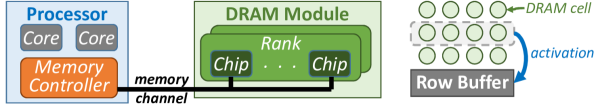
A DRAM bank typically consists of thousands of rows of cells, where each cell contains a capacitor and an access transistor. To start processing a request, the controller issues a command to activate the row containing the target address of the request (i.e., open the row to perform reads and writes), as shown in Figure 1 (right). The row buffer latches the opened row, at which point the controller sends read and write commands to the row. Each read/write command operates on one column of data at a time. Once the read and write operations to the row are complete, the controller issues a precharge command, to prepare the bank for commands to a different row. For more detail on DRAM operation, we refer the reader to our prior works (kim.isca12, ; lee.hpca13, ; lee.hpca15, ; chang.sigmetrics16, ; chang.sigmetrics17, ; lee.sigmetrics17, ; lee.pact15, ; kim.isca14, ; kim.hpca19, ; seshadri.micro17, ; liu.isca12, ; kim.hpca18, ; seshadri.bookchapter20, ).
2.2. Modern DRAM Types
We briefly describe several commonly-used and emerging DRAM types, all of which we evaluate in this work. Table 1 summarizes the key properties of each of these DRAM types. We provide more detail about each DRAM type in Appendix A.
2.2.1. DDR3 and DDR4
DDR3 (ddr3, ) is the third generation of DDRx memory, where a burst of data is sent on both the positive and negative edge of the bus clock to double the data rate. DDR3 contains eight banks of DRAM in every rank. DDR4 (ddr4, ) increases the number of banks per rank, to 16, by introducing bank groups, a new level of hierarchy in the DRAM subsystem. Due to the way in which bank groups are connected to I/O, a typical memory access takes longer in DDR4 than it did in DDR3, but the bus clock frequency is significantly higher in DDR4, which enables DDR4 to have higher bandwidth.
2.2.2. Graphics DDR5 (GDDR5)
Similar to DDR4, GDDR5 (gddr5, ) doubles the number of banks over DDR3 using bank groups. However, unlike DDR4, GDDR5 does so by increasing the die area and energy over DDR3 instead of the memory latency. GDDR5 also increases memory throughput by doubling the amount of data sent in a single clock cycle, as compared to DDR3.
2.2.3. High Bandwidth Memory (HBM)
High Bandwidth Memory (hbm, ; AMD.hbm, ) is a 3D-stacked memory (loh2008stacked, ; lee.taco16, ) that provides high throughput. designed for devices such as GPUs. Unlike GDDR5, which uses faster clock frequencies to increase throughput, HBM connects 4–8 memory channels to a single DRAM device to service many more requests in parallel.
2.2.4. Wide I/O and Wide I/O 2
Wide I/O (wideio, ) and Wide I/O 2 (wideio2, ) are 3D-stacked memories that are designed for low-power devices such as mobile phones. Similar to HBM, Wide I/O and Wide I/O 2 connect multiple channels to a single DRAM device (kim.isscc2011, ), but have fewer (2–4) channels and contain fewer banks (8) than HBM in order to lower energy consumption.
2.2.5. Hybrid Memory Cube (HMC)
The Hybrid Memory Cube (jeddeloh2012hybrid, ; pawlowski.hc11, ; rosenfeld.tr12, ; hmc.2.1, ) is a 3D-stacked memory with more design changes compared to HBM and Wide I/O. An HMC device (1) performs request scheduling inside the device itself, as opposed to relying on an external memory controller for scheduling; and (2) partitions the DRAM array into multiple vaults, which are small, vertical slices of memory of which each contains multiple banks. The vault-based structure significantly increases the amount of bank-level parallelism inside the DRAM device (with 256 banks in total), but greatly reduces the size of a row (to 256 bytes). The HMC specification (hmc.2.1, ) provides an alternate mode, which we call HMC-Alt, that uses a different address mapping than the default mode to maximize the limited spatial locality available in the smaller DRAM rows.
2.2.6. LPDDR3 and LPDDR4
LPDDR3 (lpddr3, ) and LPDDR4 (lpddr4, ) are low-power variants of DDR3 and DDR4, respectively. These DRAM types lower power consumption by using techniques such as a lower core voltage, two voltage domains on a single chip, temperature-controlled self refresh, deep power-down modes, reduced chip width, and fewer (1–2) chips per DRAM module (micronlp, ) than their standard-power counterparts. These trade-offs increase the memory access latency, and limit the total capacity of the low-power DRAM chip.
2.3. Motivation
As DRAM scaling is unable to keep pace with processor scaling, there is a growing need to improve DRAM performance. Today, conventional DDRx DRAM types suffer from three major bottlenecks. First, prior works have shown that the underlying design used by DDR3 and DDR4 remains largely the same as earlier generations of DDR memory, and as a result, the DRAM access latency has not changed significantly over the last decade (chang.sigmetrics16, ; son.isca13, ; lee.hpca13, ; lee.hpca15, ; chang.thesis17, ; lee.thesis16, ). Second, it is becoming increasingly difficult to increase the density of the memory chip, due to a number of challenges that DRAM vendors face when they scale up the size of the DRAM array (scale.imw13, ; mandelman.ibmjrd02, ; kang.memoryforum14, ; liu.isca13, ; liu.isca12, ; kim.isca14, ; mutlu.tcad19, ; mutlu.date17, ). Third, DDRx connects to the host processor using a narrow, pin-limited off-chip channel, which restricts the available memory bandwidth.
As we describe in Section 2.2, new DRAM types contain a number of key changes to mitigate one or more of these bottlenecks. Due to the non-obvious impact of such changes on application performance and energy consumption, there is a need to perform careful characterization of how various applications behave under each new DRAM type, and how this behavior compares to the application behavior under conventional DDRx architectures. Our goal in this paper is to rigorously characterize, analyze, and understand the complex interactions between several modern DRAM types and a diverse set of modern applications, through the use of detailed simulation models and new metrics that capture the sources of these interactions.
3. Methodology
We characterize the nine different DRAM types on 87 different single-threaded and multithreaded applications (spec2006, ; coral, ; coral-2, ; parsec, ; hadoop, ; ycsb, ; redis, ; Apache, ; memcached, ; difallah.vldb04, ; mediabench, ; nxp.networkaccel, ; he.pact08, ; rodinia, ; lonestar, ; IOZone, ; Netperf, ; seshadri.micro13, ), and 28 multiprogrammed workloads, using a heavily-modified version of Ramulator (kim.cal15, ), a detailed and extensible open-source DRAM simulator. Many of these applications come from commonly-used benchmark suites, including SPEC CPU2006 (spec2006, ), CORAL (coral, ) and CORAL-2 (coral-2, ), PARSEC (parsec, ), the Yahoo Cloud Suite (ycsb, ), MediaBench II (mediabench, ), Mars (he.pact08, ), Rodinia (rodinia, ), LonestarGPU (lonestar, ), IOzone (IOZone, ), and Netperf (Netperf, ).
We categorize each of our applications into one of six families: desktop/scientific (spec2006, ; coral, ; coral-2, ; parsec, ), server/cloud (hadoop, ; ycsb, ; redis, ; Apache, ; memcached, ; difallah.vldb04, ), multimedia acceleration (mediabench, ), network acceleration (nxp.networkaccel, ), GPGPU (he.pact08, ; rodinia, ; lonestar, ), and OS routines (IOZone, ; Netperf, ; seshadri.micro13, ). Tables 3–6 in Appendix C provide a complete list of the 87 applications that we evaluate. We use these 87 applications to assemble our multiprogrammed workloads, which we list in Tables 7 and 8 in Appendix C.
For our desktop/scientific and multimedia applications, we record per-core traces using Intel’s Pin software (luk2005pin, ), which uses dynamic binary instrumentation to analyze real CPU behavior at runtime. These traces are collected using a machine containing an Intel Core i7-975K processor (corei7-975.spec, ) and running the Ubuntu Server 14.04 operating system (ubuntu.14.04, ). In order to accurately record the behavior of multithreaded desktop/scientific applications, we make use of a modified Pintool (multithreadedpin.github, ), which accurately captures synchronization behavior across threads. We modify this Pintool to generate traces that are compatible with Ramulator, and to record a separate trace for each thread. In order to test the scalability of the multithreaded applications that we study (parsec, ; coral, ; coral-2, ), we run the applications and our modified Pintool on a machine that contains dual Intel Xeon E5-2630 v4 processors (xeone5-2630v4.spec, ), providing us with the ability to execute 40 threads concurrently. These machines run Ubuntu Server 14.04, and contain 128 GB of DRAM. We have open-sourced our modified Pintool (memben.github, ) along with our modified version of Ramulator (ramulator.github, ).
For our server/cloud applications and OS routines, we collect per-core traces using the Bochs full system emulator (lawton2006bochs, ) in order to record both user-mode and kernel-mode memory operations. Though prior works often overlook kernel-mode memory operations, recent studies reveal that many programs spend the majority of of their execution time in kernel mode (peter2016arrakis, ; sun2014behavior, ). Unfortunately, Pin cannot capture kernel-mode operations, so we cannot collect truly-representative traces using Pin. We use Bochs (lawton2006bochs, ) because it emulates both user-mode and kernel-mode operations. As we are constrained to using the processor models available in Bochs, we choose the Intel Core i7-2600K (corei7-2600k.spec, ), which is the closest available to the i7-975K processor (corei7-975.spec, ) we use with Pin. The emulator runs the Ubuntu Server 16.04 operating system (ubuntu.16.04, ).
Our network accelerator applications are collected from a commercial network processor (nxp.networkaccel, ). We add support in Ramulator to emulate the injection rate of requests from the network, by limiting the total number of requests that are in flight at any given time. For each workload, we evaluate four different rates: 5 in-flight requests, 10 in-flight requests, 20 in-flight requests, and 50 in-flight requests.
For GPGPU applications, we integrate Ramulator into GPGPU-Sim (bakhoda.ispass09, ), and collect statistics in Ramulator as the integrated simulator executes. We collect all results using the NVIDIA GeForce GTX 480 (gtx480.spec, ) configuration. We have open-sourced our integrated version of GPGPU-Sim and Ramulator (gpgpusimramulator.github, ).
All of the traces that we record include the delays incurred by each CPU instruction during execution, and we replay these traces with our core and cache models in Ramulator. We make several modifications to Ramulator to improve the fidelity of our experiments for all applications. We describe our modifications in Appendix B. With our modifications, Ramulator provides near-identical results (with an average error of only 6.1%; see Appendix B) to a simulator with a detailed, rigorously-validated out-of-order processor core model (gem5, ), while being significantly faster (9.8 on average for SPEC CPU2006 benchmarks; see Appendix B). We have open-sourced our modified version of Ramulator (ramulator.github, ) and a benchmark suite consisting of our application traces (memben.github, ).
Table 2 shows the system configuration parameters used for all of our experiments. For all of the DRAM types, we model a capacity, distributed across channels and ranks as listed in Table 1, and use the widely-used FR-FCFS memory scheduler (rixner.isca00, ; zuravleff.patent97, ), with 32-entry read and write queues. For all DRAM types except HMC, we use cache line interleaving (kim.isca12, ; jeong.hpca12, ; kim.hpca10, ; zhang.micro00, ; rokicki.tr96, ) for the physical address, where consecutive cache lines are interleaved across multiple channels (and then across multiple banks within a channel) to maximize the amount of memory-level parallelism. Cache line interleaving is used by processors such as the Intel Core (coregen7.datasheet, ), Intel Xeon (xeone5.datasheet, ; lenovo.xeon.memconfig, ), and IBM POWER9 (power9.datasheet, ) series. The HMC specification (hmc.2.1, ) explicitly specifies two fixed interleavings for the physical address. The first interleaving, which is the default for HMC, interleaves consecutive cache lines across multiple vaults, and then across multiple banks. The second interleaving, which we use for HMC-Alt (see Section 2.2.5), interleaves consecutive cache lines only across multiple vaults. For each DRAM type currently in production, we select the fastest frequency variant of the DRAM type on the market today (see Table 1 for key DRAM properties), as we can find reliable latency and power information for these products. As timing parameters for HMC have yet to be publicly released, we use the information provided in prior work (kim2013memory, ; jeddeloh2012hybrid, ) to model the latencies.
| Processor |
x86-64 ISA, 128-entry instruction window, 4-wide issue
single-threaded/multiprogrammed: 4 cores, multithreaded: 20 cores, 2 threads per core, |
|---|---|
| Caches |
per-core L1: , 4-way set associative
per-core L2: , 4-way set associative shared L3: for every core, 8-way set associative |
| Memory | 32/32-entry read/write request queues, FR-FCFS (rixner.isca00, ; zuravleff.patent97, ), |
| Controller | open-page policy, cache line interleaving (kim.isca12, ; jeong.hpca12, ; kim.hpca10, ; zhang.micro00, ; rokicki.tr96, ) |
We integrate DRAMPower (drampower, ), an open-source DRAM power profiling tool, into Ramulator such that it can perform power profiling while Ramulator executes. To isolate the effects of DRAM behavior, we focus on the power consumed by DRAM instead of total system power. We report power numbers only for the DRAM types for which vendors have publicly released power consumption specifications (micron.ddr3.2gb.datasheet, ; micron.ddr4.4gb.datasheet, ; micron.lpddr3.8gb.datasheet, ; micron.lpddr4.8gb.datasheet, ; hynix.gddr5.2gb.datasheet, ), to ensure the accuracy of the results that we present.
4. Characterization Metrics
Performance Metrics. We measure single-threaded application performance using instructions per cycle (IPC). For multithreaded applications, we show parallel speedup (i.e., the single-threaded execution time divided by the parallel execution time), which accounts for synchronization overheads. For multiprogrammed workloads, we use weighted speedup (snavely.asplos00, ), which represents the job throughput (eyerman.ieeemicro08, ). We verify that trends for other metrics (e.g., harmonic speedup (luo.ispass01, ), which represents the inverse of the job turnaround time) are similar. To quantify the memory intensity of an application, we use the number of misses per kilo-instruction (MPKI) issued by the last-level cache for that application to DRAM.
Our network accelerator workloads are collected from a commercial network processor (nxp.networkaccel, ), which has a microarchitecture different from a traditional processor. We present performance results for the network accelerator in terms of sustained memory bandwidth.
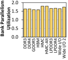
Parallelism Metrics. Prior works have used either memory-level parallelism (MLP) (glew.waci98, ; chou.isca04, ; tuck.micro06, ; qureshi.isca06, ; mutlu.isca05, ) or bank-level parallelism (BLP)] (mutlu.isca08, ; tang.micro16, ; lee.micro09, ; kim.micro10, ) to quantify the amount of parallelism across memory requests. Unfortunately, neither metric fully represents the actual parallelism exploited in DRAM. MLP measures the average number of outstanding memory requests for an application, but this does not capture the amount of parallelism offered by the underlying hardware. BLP measures the average number of memory requests that are actively being serviced for a single thread during a given time interval. While BLP can be used to compare the bank parallelism used by one thread within an interval to the usage of another thread, it does not capture the average bank parallelism exploited by all concurrently-executing threads and applications across the entire execution, which can provide insight into whether the additional banks present in by many of the DRAM types (compared to DDR3) are being utilized.
We define a new metric, called bank parallelism utilization (BPU), which quantifies the average number of banks in main memory that are being used concurrently. To measure BPU, we sample the number of active banks for every cycle that the DRAM is processing a request, and report the average utilization of banks:
| (1) |
A larger BPU indicates that applications are making better use of the bank parallelism available in a particular DRAM type. Unlike MLP and BLP, BPU fully accounts for (1) whether requests from any thread contend with each other for the same bank, and (2) how much parallelism is offered by the memory device. As we see in our analysis (Sections 5–9), BPU helps explain why some memory-intensive applications do not benefit from high-bandwidth memories such as HMC, while other memory-intensive applications do benefit.
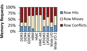
Contention Metrics. An important measure of spatial and temporal locality in memory is the row buffer hit rate, also known as row buffer locality. To quantify the row hit rate, prior works count the number of row buffer hits and the number of row buffer misses, which they define as any request that does not hit in the currently-open row. Unfortunately, this categorization does not distinguish between misses where a bank does not have any row open, and misses where a bank is currently processing a request to a different row (i.e., a row buffer conflict). This distinction is important, as a row buffer conflict typically takes longer to service than a row buffer miss, as a conflict must wait to issue a precharge operation, and may also need to wait for an earlier request to the bank to complete. A row buffer conflict takes at least as much as double the row miss latency, when the conflicting request arrives just after a request with a row miss starts accessing the DRAM. Table 1 lists the minimum row buffer conflict latency for each DRAM type, assuming that no prior memory request has already issued the precharge operation for the conflicting row. Note that if there is more than one pending memory request that needs to access the conflicting row, the row buffer conflict latency could be even higher.
To accurately capture row buffer locality, we introduce a new characterization methodology where we break down memory requests into: (1) row buffer hits; (2) row buffer misses, which only include misses for a DRAM request where the bank does not have any row open; and (3) row buffer conflicts, which consist of misses where another row is currently open in the bank and must be closed (i.e., precharged) first. Row buffer conflicts provide us with important information about how the amount of parallelism exposed by a DRAM type can limit opportunities to concurrently serve multiple memory requests, which in turn hurts performance.
5. Single-Threaded/Multiprogrammed Desktop and Scientific Programs
We first study the memory utilization, performance, and DRAM energy consumption of our tested DRAM types on single-threaded desktop and scientific applications from the SPEC 2006 benchmark suite (spec2006, ), and on multiprogrammed bundles of these applications.
5.1. Workload Characteristics
Using the DDR3 memory type, we study the memory intensity of each workload. The workloads encompass a wide range of intensity, with some CPU-bound applications (e.g., gamess, calculix) issuing memory requests only infrequently, and other memory-bound applications (e.g., mcf) issuing over 15 last-level cache (i.e., L3) misses per kilo-instruction (MPKI). The workloads also exhibit a large range of row buffer locality, with row buffer hit rates falling anywhere between 2.4–53.1% (see Appendix D.1).
We study the relationship between the performance (IPC) and memory intensity (MPKI) of the desktop and scientific applications (see Appendix D.1 for details and plots). In general, we observe that the IPC decreases as the MPKI increases, but there are two notable exceptions: namd and gobmk. To understand these exceptions, we study the amount of bank parallelism that an application is able to exploit by using the BPU metric we introduced in Section 4 (see Appendix D.1 for BPU values for all applications). In our configuration, DDR3 has 32 banks spread across four memory channels. For most applications with low memory intensity (i.e., MPKI 4.0), the BPU for DDR3 is very low (ranging between 1.19 and 2.01) due to the low likelihood of having many concurrent memory requests. The two exceptions are namd and gobmk, which have BPU values of 4.03 and 2.91, respectively. The higher BPU values at low memory intensity imply that these applications exhibit more bursty memory behavior, issuing requests in clusters. Thus, they could benefit more when a DRAM type offers a greater amount of bank parallelism (compared to a DRAM type that offers reduced latency).
From the perspective of memory, we find that there is no discernible difference between applications with predominantly integer computation and applications with predominantly floating point computation (see Appendix D.1). As a result, we do not distinguish between the two in this section.
5.2. Single-Thread Performance
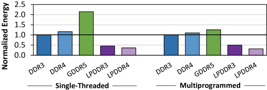
Figure 2 (top) shows the performance of the desktop workloads under each of our standard-power DRAM types, normalized to the performance of each workload when using a DDR3-2133 memory. Along the x-axis, the applications are sorted by MPKI, from least to greatest. We make two observations from these experiments.
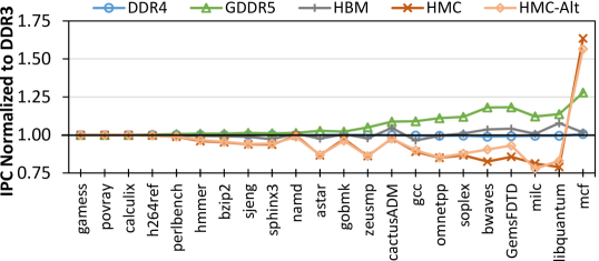
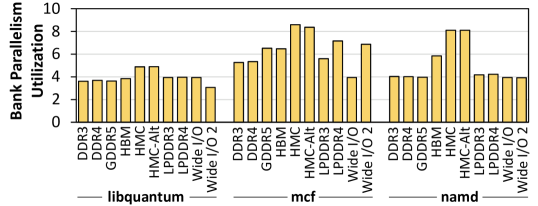
Even though DDR4 has 50% higher bandwidth than DDR3 and contains double the number of banks (64 in our four-channel DDR4 configuration vs. 32 in our four-channel DDR3 configuration), DDR4 performs 0.2% worse than DDR3, on average across all of our desktop and scientific applications, as we see in Figure 2 (top). The best performance with DDR4 is for mcf, with an improvement of only 0.5% over DDR3. We find that both major advantages of DDR4 over DDR3 (i.e., greater bandwidth, more banks) are not useful to our applications. Figure 3 shows the BPU for three representative workloads (libquantum, mcf, and namd). Across all of our applications, we find that there is not enough BPU to take advantage of the 32 DDR3 banks, let alone the 64 DDR4 banks. mcf has the highest BPU, at 5.33 in DDR4, still not enough to benefit from the additional banks. Instead, desktop and scientific applications are sensitive to the memory latency. Applications are hurt by the increased access latency in DDR4 (11/14% higher in DDR4 for a row hit/miss than in DDR3), which is a result of the bank group organization (which does not exist in DDR3; see Section 2.2).
and is not highly memory intensive.
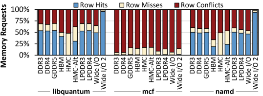
From Figure 2 (top), we observe that few standard-power DRAM types can improve performance across all desktop and scientific applications over DDR3. Notably, we find that HMC actually results in significant slowdowns over DDR3 for most of our single-threaded applications. Averaged across all workloads, HMC performs 5.8% worse than DDR3. To understand why, we examine the row buffer locality of our applications when running with different memory types. Recall from Section 2.2 that HMC reduces row buffer locality in exchange for a much greater number of banks (256 in HMC vs. 32 in DDR3) and much greater bandwidth (4.68 the bandwidth of DDR3). We already see in Figure 3 that, with the exception of mcf, HMC cannot provide significant BPU increases for our single-threaded applications, indicating that the applications cannot take advantage of the increased bank count and higher bandwidth.
Figure 4 shows the row buffer locality (see Section 4) for our three representative applications. As we observe from the figure, HMC eliminates nearly all of the row hits that other memories attain in libquantum and namd. This is a result of the row size in HMC, which is 97% smaller than the row size in DDR3. This causes many more row misses to occur, without significantly affecting the number of row conflicts. As a result, the average memory request latency (across all applications) in HMC is 25.6% higher than that in DDR3. The only application with a lower average memory request latency in HMC is mcf, because the majority of its memory requests in all DRAM types are row conflicts (see middle graph in Figure 4). Thus, due to its low spatial locality and high BPU, mcf is the only application that sees a significant speedup with HMC (63.4% over DDR3).
Unlike HMC, GDDR5 successfully improves the performance of all of our desktop and scientific applications with higher memory intensity. This is because GDDR5 delivers higher bandwidth at a lower latency than DDR3 (see Table 1), which translates into an average performance improvement of 6.4%. In particular, for applications with high memory intensity (i.e., MPKI 15.0), GDDR5 has an average speedup of 16.1%, as these applications benefit most from a combination of higher memory bandwidth and lower memory request latencies.
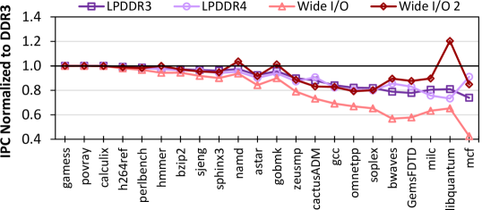
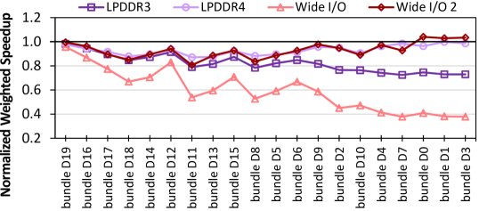
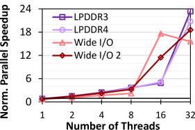
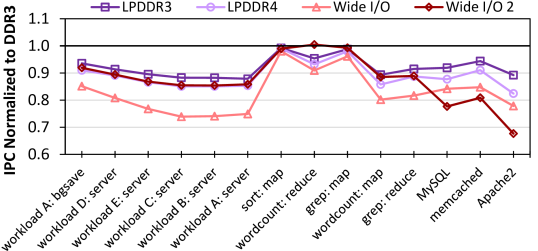
Figure 2 (bottom) shows the performance of the desktop and scientific applications when we use low-power or mobile DRAM types. In general, we note that as the memory intensity (i.e., MPKI) of an application increases, its performance with low-power memory decreases compared to DDR3. In particular, LPDDR3 and LPDDR4 perform worse because they take longer to complete a memory request, increasing the latency for a row miss over DDR3 and DDR4 by 53.2% and 50.0%, respectively (see Table 1). Wide I/O DRAM performs significantly worse than the other DRAM types, as (1) its much lower clock frequency greatly restricts its overall throughput, and (2) its row hit latency is longer. Wide I/O 2 offers significantly higher row buffer locality and lower hit latency than Wide I/O. As a result, applications such as namd and libquantum perform well under Wide I/O 2.
We conclude that even though single-threaded desktop and scientific applications display a wide range of memory access behavior, they generally need DRAM types that offer (1) low access latency and (2) high row buffer locality.
5.3. Multiprogrammed Workload Performance
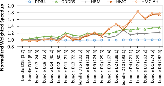
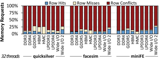
We combine the single-threaded applications into 20 four-core multiprogrammed workloads (see Table 7 in Appendix C for workload details), to study how the memory access behavior changes. Figure 5 shows the performance of the workloads (sorted by MPKI) with each DRAM type. We draw out three findings from the figure.
due to a combination of high BPU and poor row buffer locality.
First, for multiprogrammed workloads, HMC performs better than the other DRAM types despite its significantly smaller row buffer size. On average, HMC improves system performance (as measured by weighted speedup) by 17.0% over DDR3. Note that while some workloads do very well under HMC (with the greatest performance improvement being 83.1% for bundle D7), many workloads with lower memory intensity (i.e., MPKI 70) still perform slightly worse than they do under DDR3 (with the greatest performance loss being 3.4% for bundle D12). We find two major reasons for HMC’s high performance with multiprogrammed workloads: poor row buffer locality and high BPU.
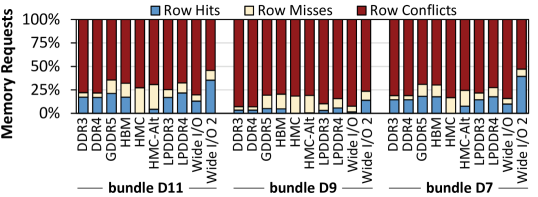
The row buffer locality of the multiprogrammed workloads is much lower than that of the single-threaded applications. Figure 6 shows row buffer locality for three representative workloads. For bundle D9, which has an MPKI of 167.4, the row buffer hit rate never exceeds 5.6% on any DRAM type. We observe that for all of our workloads, the vast majority of memory accesses are row conflicts. This is because each application in a multiprogrammed workload accesses a different address space, and these competing applications frequently interfere with each other when they conflict in banks or channels within the shared DRAM, as also observed in prior works (kim.isca12, ; hassan.hpca16, ; hassan.isca19, ; lee.hpca13, ).
With HMC, we find that the BPU of highly-memory-intensive workloads is significantly higher than the BPU with DDR3. Figure 7 shows the BPU for the three representative workloads. Bundle D11, which has an MPKI of 71.3, does not issue enough parallel memory requests, limiting its BPU. For bundle D7, which has a much higher MPKI of 229.3, concurrent memory requests are distributed across the memory address space, as three out of the four applications in the workload (libquantum, mcf, and milc) are memory intensive (i.e., MPKI 4.0 for single-threaded applications). As a result, with HMC, the workload achieves 2.05 the BPU that it does with DDR3.
Second, unlike HMC, which does not perform well for most non-memory-intensive multiprogrammed workloads, GDDR5 improves performance for all 20 of our multiprogrammed workloads. This is because GDDR5 provides a balanced combination of low memory latencies, high bank parallelism, and high bandwidth. However, GDDR5’s balance across these metrics is not enough to maximize the performance of our highly-memory-intensive workloads, which require very high bandwidth, and thus GDDR5’s average performance improvement over DDR3 on multiprogrammed workloads, 13.0%, is lower than that of HMC (17.0%).
Third, some low-power DRAM types can provide energy savings (see Section 5.4) for multiprogrammed workloads without sacrificing performance. From Figure 5 (bottom), we observe that LPDDR4 and Wide I/O 2 perform competitively with DDR3 for highly-memory-intensive workloads. This is because both DRAM types provide higher amounts of parallelism and bandwidth than DDR3, and the highly-memory-intensive applications make significant use of the available parallelism and memory bandwidth, which lowers application execution time. As a result, such applications are not significantly impacted by the increased memory access latency in LPDDR4 and Wide I/O 2.
We conclude that for multiprogrammed workloads, DRAM types that provide high bank parallelism and bandwidth can significantly improve performance when a workload exhibits (1) high memory intensity, (2) high BPU, and (3) poor row buffer locality.
5.4. DRAM Energy Consumption
We characterize the energy consumption of our desktop and scientific workloads for the DRAM types that we have accurate power models for (i.e., datasheet values for power consumption that are provided by vendors for actual off-the-shelf parts). Figure 8 shows the average DRAM energy consumption by DDR3, DDR4, GDDR5, LPDDR3, and LPDDR4 for our single-threaded applications and multiprogrammed workloads, normalized to the energy consumption of DDR3. We make two new observations from the figure.
For all of our desktop/scientific workloads, LPDDR3/4 consume significantly less energy than DDR3/4 due to the numerous low-power features incorporated in their design (see Section 2.2). In particular, as we discuss in Appendix E, standby power is the single largest source of power consumption for these workloads, and LPDDR3/4 incorporate a number of optimizations to reduce standby power. Unfortunately, these optimizations lead to increased memory request latencies (see Table 1). This, in turn, hurts the overall performance of single-threaded applications, as we see in Figure 2 (bottom). GDDR5 makes the opposite trade-off, with reduced memory request latencies and thus higher performance, but at the cost of 2.15 more energy than DDR3 for single-threaded applications.
For multiprogrammed workloads, LPDDR4 delivers a 68.2% reduction in energy consumption, on average across all workloads, while losing only 7.0% performance compared to DDR3 (see Section 5.3). This is because LPDDR4 compensates for its higher memory request latency over DDR3 by having a greater number of banks. As we discuss in Section 5.3, highly-memory-intensive multiprogrammed workloads can achieve a high BPU, which allows them to take advantage of the increased bank parallelism available in LPDDR4. As a comparison, LPDDR3 still performs poorly with these workloads because it has lower bandwidth and a lower bank count than LPDDR4. In contrast, GDDR5 provides higher throughput than LPDDR4, and due to the high memory intensity of multiprogrammed workloads, the workloads complete much faster with GDDR5 than DDR3 (13.0% higher performance on average; see Section 5.3). The increased performance of GDDR5 comes at the cost of consuming only 25.6% more energy on average than DDR3, which is a much smaller increase than what we observe for the single-threaded applications.
We conclude that (1) low-power DRAM variants (LPDDR3/4) are effective at reducing overall DRAM energy consumption, especially for applications that exhibit high BPU; and (2) the performance improvements of GDDR5 come with a significant energy penalty for single-threaded applications, but with a smaller penalty for multiprogrammed workloads.
6. Multithreaded Desktop and Scientific Programs
Many modern applications, especially in the high-performance computing domain, launch multiple threads on a machine to exploit the thread-level parallelism available in multicore systems. We evaluate the following applications:
-
•
blackscholes, canneal, fluidanimate, raytrace, bodytrack, facesim, freqmine, streamcluster, and swaptions from PARSEC 3.0 (parsec, ), and
- •
6.1. Workload Characteristics
Multithreaded workloads often work on very large datasets (e.g., several gigabytes in size) that are partitioned across the multiple threads. A major component of multithreaded application behavior is how the application scales with the number of threads. This scalability is typically a function of (1) how memory-bound an application is, (2) how much synchronization must be performed across threads, and (3) how balanced the work done by each thread is.
We provide a detailed experimental analysis of the IPC and MPKI of the multithreaded applications in Appendix D.2. From the analysis, we find that these applications have a narrower IPC range than the single-threaded desktop applications. This is often because multithreaded applications are designed to strike a careful balance between computation and memory usage, which is necessary to scale the algorithms to large numbers of threads. Due to this balance, memory-intensive multithreaded applications have significantly higher IPCs compared to memory-intensive single-threaded desktop/scientific applications, even as we scale the number of threads. For example, the aggregate MPKI of miniFE increases from 11.5 with only one thread to 68.1 with 32 threads, but its IPC per thread remains around 1.5 (for both one thread and 32 threads). The relatively high IPC indicates that the application is not completely memory-bound even when its MPKI is high.
6.2. Performance
To study performance and scalability, we evaluate 1, 2, 4, 8, 16, and 32 thread runs of each multithreaded application on each DRAM type. All performance plots show parallel speedup, normalized to one-thread execution on DDR3, on the y-axis, and the thread count (in log scale) on the x-axis. For brevity, we do not show individual results for each application. We find that the applications generally fall into one of three categories: (1) memory-agnostic, where the application is able to achieve near-linear speedup across most thread counts for all DRAM types; (2) throughput-bound memory-sensitive, where the application is highly memory-intensive, and has trouble approaching linear speedup for most DRAM types; and (3) irregular memory-sensitive, where the application is highly memory-intensive, and its irregular memory access patterns allow it to benefit from either lower memory latency or higher memory throughput.
Memory-Agnostic Applications. Six of our applications are memory-agnostic: blackscholes, raytrace, swaptions, quicksilver, pennant, and streamcluster. Figure 9 shows the performance of quicksilver across all thread counts, which is representative of the memory-agnostic applications. We draw out three findings from the figure.
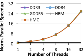
First, regardless of the DRAM type, the performance of quicksilver scales well with the thread count, with no tapering of performance improvements for the standard-power DRAM types (i.e., DDR3/4, GDDR5, HBM, HMC). This is because memory-agnostic applications have relatively low MPKI values (see Appendix D.2), even at high thread counts (e.g., quicksilver has an MPKI of 20.9 at 32 threads). Therefore, all of the standard-power DRAM types are able to keep up as the thread counts increase, and the memory-agnostic applications do not benefit significantly from one DRAM type over another.
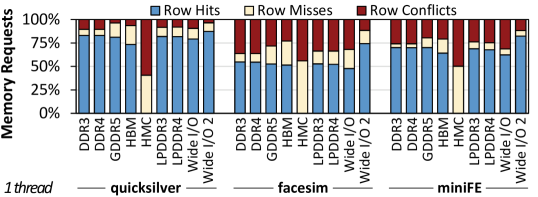
Second, like many of our memory-agnostic applications, quicksilver does not have a fully-linear speedup at 32 threads. This is because when the number of threads increases from 1 to 32, the row hit rate decreases significantly (e.g., for DDR3, from 83.1% with one thread to 7.2% with 32 threads), as shown in Figure 10, due to contention among the threads for shared last-level cache space and shared DRAM banks. The significantly lower row hit rate results in an increase in the average memory request latency. Two of our memory-agnostic applications (swaptions and pennant) maintain higher row hit rates (e.g., 46.6% for pennant at 32 threads; not shown) because they have significantly lower memory intensity (i.e., MPKI 3 at 32 threads) than our other memory-agnostic applications, generating less contention at the last-level cache and DRAM banks. As a result, these two applications have a fully-linear speedup at 32 threads.
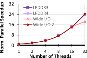
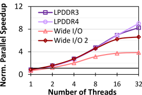
Third, due to the memory-agnostic behavior of these applications, there is no discernible difference in performance between standard-power DRAM types, LPDDR3/4, and Wide I/O 2. Given the minimal memory needs of these applications, the increased latencies and reduced bandwidth of low-power DRAM types do not have a significant impact on the applications in most cases.111The one exception is Wide I/O, for which performance scaling begins to taper off at 32 threads. Wide I/O’s poor scalability is a result of its combination of high memory access latency and a memory bandwidth that is significantly lower than the other DRAM types (see Table 1). Based on these observations, we believe that the LPDDR3/4 and Wide I/O 2 low-power DRAM types are promising to use for memory-agnostic applications, as they can lower the DRAM power consumption with little impact on performance.
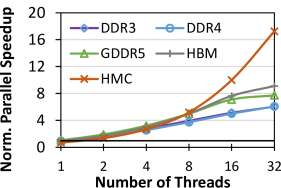
Throughput-Bound Memory Sensitive Applications. Five of our applications are throughput-bound memory-sensitive: bodytrack, canneal, fluidanimate, facesim, and freqmine. Figure 11 shows the performance of facesim across all thread counts, which is representative of the throughput-bound memory-sensitive applications. These applications become highly memory-intensive (i.e., they have very high aggregate MPKI values) at high thread counts. As more threads contend for the limited shared space in the last-level cache, the cache hit rate drops, placing greater pressure on the memory system. This has two effects. First, since the memory requests are generated across multiple threads, where each thread operates on its own working set of data, there is little spatial locality among the requests that are waiting to be serviced by DRAM at any given time. As we see in Figure 10, facesim does not exploit row buffer locality at 32 threads. Second, because of their high memory intensity and poor spatial locality, these applications benefit greatly from a memory like HMC, which delivers higher memory-level parallelism and higher bandwidth than DDR3 at the expense of spatial locality and latency. As Figure 11 shows, (1) the performance provided by the other memories cannot scale at the rate provided by HMC at higher thread counts; and (2) HMC outperforms even GDDR5 and HBM, which in turn outperform other DRAM types.
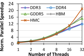
Irregular Memory-Sensitive Applications. Only one application is irregular memory-sensitive: miniFE. Figure 12 shows the performance of miniFE across all thread counts. miniFE operates on sparse matrices, which results in irregular memory access patterns that compilers cannot easily optimize. One result of this irregular behavior is low BPU at all thread counts, corroborating similar observations by prior work (tang.micro16, ) for miniFE and other irregular multithreaded workloads. As a result, for smaller problem sizes (e.g., 32 x 32 x 32 for miniFE), miniFE becomes memory-latency-bound, and behaves much like our single-threaded desktop applications in Section 5. We draw out two findings from Figure 12. First, miniFE with a 32 x 32 x 32 problem size benefits most from traditional, low-latency memories such as DDR3/4 and GDDR5, while it fails to achieve such high benefits with throughput-oriented memories such as HMC and HBM. In fact, just as we see for memory-agnostic applications, many of the low-power memories outperform HMC and HBM at all thread counts. Second, as the core count increases, miniFE benefits more from high memory throughput and high bank-level parallelism. As a result, while the performance improvement with DDR3 starts leveling off after 16 threads, the performance improvements with HBM and with HMC continue to scale at 32 threads. Unlike DDR3, DDR4 continues to scale as well, as DDR4 provides higher throughput and more banks than DDR3.
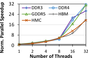
The irregular behavior of miniFE changes as the problem size grows. Figure 13 shows the performance of miniFE as we increase the problem size to 64 x 64 x 64. We observe that as the number of threads increases, the scaling trends look significantly different than they do for the smaller 32 x 32 x 32 problem size (Figure 12). For reference, with a single thread and with the DDR3 DRAM type, the 64 x 64 x 64 problem size takes 13.6x longer than the 32 x 32 x 32 problem size. The larger problem size puts more pressure on the cache hierarchy and the memory subsystem (e.g., the memory footprint increases by 449%; see Table 3 in Appendix C), which causes miniFE to transition from memory-latency-bound to memory-throughput-bound. As a result, when the number of threads increases, lower-throughput DRAM types such as DDR3 and DDR4 become the bottleneck to scalability, limiting parallel speedup at 32 threads to only 6.1x. Likewise, we observe that all of our low-power DRAM types cannot deliver the throughput required by miniFE at high thread counts. In contrast, HMC can successfully take advantage of the high throughput and high contention between threads, due to its large number of banks and high bandwidth. As a result, HMC reaches a parallel speedup of 17.3x at 32 threads, with no drop-off in its scalability as the number of threads increases from 1 to 32. This behavior is similar to what we observe for throughput-bound memory-sensitive applications (e.g., the performance of facesim in Figure 11).
depends on the problem size.
At small problem sizes, these applications are latency-bound, and thus benefit from DRAM types that provide low latency.
As the problem size increases, these applications become throughput-bound, behaving like the throughput-bound memory-sensitive applications, and thus benefit from DRAM types that provide high throughput.
We conclude that the ideal DRAM type for a multithreaded application is highly dependent on the application behavior, and that for many such applications, such as memory-agnostic or irregular memory-sensitive applications with smaller problem sizes, low-power DRAM types such as LPDDR4 can perform competitively with standard-power DRAM types.
7. Server and Cloud Workloads
Server and cloud workloads are designed to accommodate very large data sets, and can often coordinate requests between multiple machines across a network. We evaluate the following workloads with representative inputs:
-
•
the map and reduce tasks (mapreduce, ) for grep, wordcount, and sort, implemented using Hadoop (hadoop, ) for scalable distributed processing (we use four map threads for each application);
- •
-
•
an Apache server (Apache, ), which services a series of wget requests from a remote server;
-
•
Memcached (memcached, ), using a microbenchmark that inserts key-value pairs into a memory cache; and
-
•
the MySQL database (difallah.vldb04, ), using a microbenchmark that loads the sample employeedb database.
7.1. Workload Characteristics
From our analysis, we find that while server and cloud workloads tend to work on very large datasets (e.g., gigabytes of data), the workloads are written to maximize the efficiency of their on-chip cache utilization. As a result, these applications only infrequently issue requests to DRAM, and typically exhibit low memory intensity (i.e., MPKI 10) and high IPCs. We show IPC plots for these workloads in Appendix D.3.
For each of our Hadoop applications, we find that the four map threads exhibit near-identical behavior. As a result, we show the characterization of only one out of the four map threads (map 0) in the remainder of this section.
7.2. Single-Thread Performance
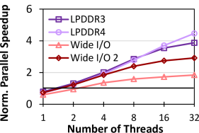
Figure 14 shows the performance of single-threaded applications for server and cloud environments when run on our evaluated DRAM types, normalized to DDR3. We find that none of our workloads benefit significantly from using HBM, HMC, or Wide I/O 2. These DRAM types sacrifice DRAM latency to provide high throughput. Since our workloads have low memory bandwidth needs, they are unable to benefit significantly from this additional throughput.
To understand why high-throughput memories do not benefit these applications, we focus on YCSB (the leftmost six workloads in Figure 14). For these workloads, we observe that as the memory intensity increases, HMC performs increasingly worse compared to DDR3. We find that the YCSB workloads exhibit low BPU values (never exceeding 1.80). Figure 15 shows the BPU (left) and row buffer locality (right) for workload A: server, as a representative YCSB workload. Due to the low BPU of the workload across all DRAM types, the high number of banks provided by HBM, HMC, and Wide I/O are wasted. HMC also destroys the row hits (and thus lower access latencies) that other DRAM types provide, resulting in a significant performance loss of 11.6% over DDR3, on average across the YCSB workloads. HMC avoids performance loss for applications that have high BPU, such as the map process for grep (with a BPU of 18.3; not shown). However, such high BPU values are not typical for the server and cloud workloads we examine.
We find two effects of the low memory intensity and low BPU of server and cloud workloads. First, these workloads are highly sensitive to memory request latency. The limited memory-level parallelism exposes the latency of a memory request to the processor pipeline (ghose.isca13, ; qureshi.isca06, ; mutlu.hpca03, ; mutlu.micro07, ; mutlu.ieeemicro06, ; kirman.hpca05, ; das.micro09, ). Second, the performance loss due to using the low-power DRAM types is mainly due to the increased memory access latencies, and not reduced throughput. For example, as we observe in Figure 14 (bottom), Wide I/O’s performance loss is comparable to the performance loss with other low-power DRAM types for many of our server and cloud workloads, even though the available bandwidth of Wide I/O is only 25% of the bandwidth available with LPDDR4 (see Table 1).
We conclude that the server and cloud workloads we evaluate are highly sensitive to the memory access latency, and are not significantly impacted by memory throughput.
7.3. Multiprogrammed Performance
We combine the single-threaded server and cloud applications into eight four-core multiprogrammed workloads (see Table 8 in Appendix C for workload details). Figure 16 shows the performance of executing four-core multiprogrammed workloads for our YCSB workload bundles (Y0–Y4) and Hadoop workload bundles (H0–H2) with each DRAM type. We identify two trends from the figure.
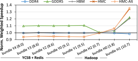
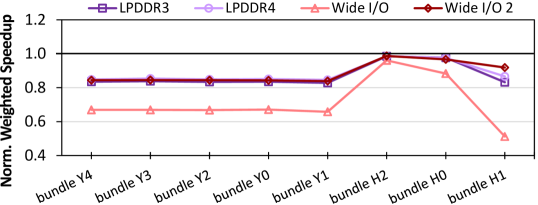
First, we observe that the multiprogrammed YCSB workloads see little benefit from high-throughput memories, much like the single-threaded YCSB applications. One exception to this is when the workloads run on GDDR5, which provides a mean speedup of 10.2% over DDR3 due to the increased memory intensity (and thus higher memory bandwidth demand) of the multiprogrammed workloads. On low-power DRAM types, the multiprogrammed YCSB workloads experience larger performance drops over DDR3 than the single-threaded applications. For LPDDR3, LPDDR4, and Wide I/O 2, the performance drop ranges between 14.5% and 17.2%. For Wide I/O, the performance drop is even worse, with an average drop of 33.3%. Because the multiprogrammed workloads are more memory-intensive than the single-threaded applications, the reduced throughput of low-power DRAM types compared to DDR3 has a greater negative impact on the multiprogrammed workloads than on the single-threaded applications.
Second, we observe that HMC significantly improves the performance of the Hadoop workloads, because the working sets of the individual applications in each workload conflict with each other in the last-level CPU cache. This increases the last-level cache miss rate, which in turn significantly increases the memory intensity compared to the memory intensity of the single-threaded Hadoop applications. Due to the increased memory intensity, the queuing latency of memory requests make up a significant fraction of the DRAM access latency. For example, on DDR3, queuing accounts for 77.2% of the total DRAM access latency for workload H0 (not shown). HMC is able to alleviate queuing significantly for the multiprogrammed Hadoop workloads compared to DDR3 (reducing it to only 23.8% of the total DRAM access latency), similar to what we saw for multiprogrammed desktop and scientific workloads in Section 5.3. On average, with HMC, the Hadoop workloads achieve 2.62 the BPU, with an average performance improvement of 9.3% over DDR3.
We conclude that the performance of multiprogrammed server and cloud workloads depends highly on the interference that occurs between the applications in the workload, and that HMC provides performance benefits when such application interference results in high memory intensity.
7.4. DRAM Energy Consumption
Figure 17 shows the DRAM energy consumption for the single-threaded and multiprogrammed server and cloud workloads. GDDR5 consumes a significant amount of energy (2.65 the energy consumed by DDR3 for single-threaded applications, and 2.23 for multiprogrammed workloads). Given the modest performance gains over DDR3 (3.8% for single-threaded applications, and 9.4% for multiprogrammed workloads), GDDR5 is much less energy efficient than DDR3. This makes GDDR5 especially unsuitable for a datacenter setting, where energy consumption and efficiency are first-order design concerns. In contrast, we find that LPDDR3/LPDDR4 save a significant amount of DRAM energy (58.6%/61.6% on average), while causing only relatively small performance degradations for single-threaded applications compared to DDR3 (8.0%/11.0% on average). Thus, we believe LPDDR3 and LPDDR4 can be competitive candidates for the server and cloud environments, as they have higher memory energy efficiency than DDR3.
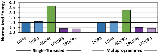
We conclude that low-power DRAM types can be viable options to improve energy efficiency in server and cloud environments, while DRAM types such as GDDR5 are not as energy efficient as DDR3.
8. Heterogeneous System Workloads
In this section, we study the performance and energy consumption of workloads that are representative of those that run on three major types of processors and accelerators in heterogeneous systems, such as systems-on-chip (SoCs) and mobile processors: (1) multimedia acceleration, which we approximate using benchmarks from the MediaBench II suite for JPEG-2000 and H.264 video encoding and decoding (mediabench, ); (2) network acceleration, for which we use traces collected from a commercial network processor (nxp.networkaccel, ); and (3) general-purpose GPU (GPGPU) applications from the Mars (he.pact08, ), Rodinia (rodinia, ), and LonestarGPU (lonestar, ) suites.
8.1. Multimedia Workload Performance
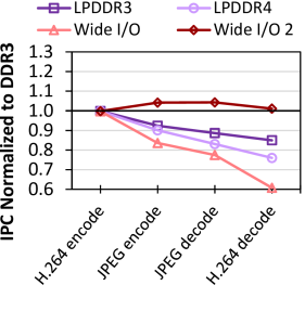
Multimedia accelerators are designed to perform high-throughput parallel operations on media content, such as video, audio, and image processing (mediabench, ). Often, the content is encoded or decoded in a streaming manner, where pieces of the content are accessed from memory and processed in order. Multimedia accelerators typically work one file at a time, and tend to exhibit high spatial locality due to the streaming behavior of their algorithms. The algorithms we explore are often bound by the time required to encode or decode each piece of media (e.g., a video frame). We find that JPEG processing and H.264 encoding applications are highly compute-bound (i.e., MPKI 5.0), and exhibit very slow streaming behavior (i.e., the requests are issued in a streaming fashion, but exhibit low memory intensity). In contrast, we find that H.264 decoding exhibits a highly memory-bound fast streaming behavior, with an MPKI of 124.5.
Figure 18 shows the performance of the multimedia applications on each DRAM type, normalized to DDR3. We draw out two findings from the figure. First, JPEG encoding/decoding and H.264 encoding do not benefit from any of the high-bandwidth DRAM types, due to the applications’ low memory intensity. The performance of some of these applications is actually hurt significantly by HMC, due to HMC’s small row size and high access latencies. In contrast, the larger row width of Wide I/O 2 allows these applications to experience modest speedups over DDR3, by increasing the row hit rate.
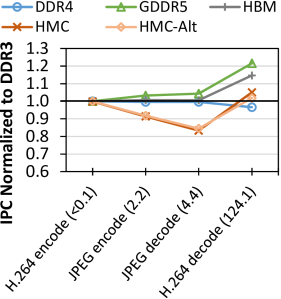
Second, unlike the other multimedia applications, H.264 decoding performs significantly better with certain high-bandwidth memories: with GDDR5/HBM, its performance improves by 21.6%/14.7% over DDR3. We find that GDDR5 and HBM cater well to H.264 decoding, as the application exhibits high memory intensity with highly-localized streaming access patterns, causing the majority of its memory requests to be row hits. Due to its streaming nature, H.264 decoding still relies heavily on DRAM types with wide rows, which can take advantage of spatial locality. As a result, even though the BPU of H.264 decoding increases in HMC by 177.2% over DDR3 (due to the distribution of streaming requests across multiple banks), the application does not see large performance improvements with HMC. The highly-localized access pattern also hurts the performance of H.264 decoding with DDR4. Much like with DDR3, the application’s memory requests exploit spatial locality within a DDR4 DRAM row, but make use of only a limited amount of bank parallelism. As a result, the application cannot take advantage of the additional banks in DDR4 over DDR3, and DDR4 slows down H.264 decoding by 2.6% compared to DDR3 due to its increased access latency.
8.2. Network Accelerator Performance
The network accelerators we study handle a number of data processing tasks (e.g., processing network packets, issuing network responses, storing the data in an application buffer). Such network accelerators can be found in dedicated network processing chips, SoCs, and server chips (nxp.networkaccel, ). Unlike multimedia accelerators, which exhibit regular streaming access patterns, network accelerator memory access patterns are dependent on the rate of incoming network traffic. A network accelerator monitors traffic entering from the network adapter, performs depacketization and error correction, and transfers the data to the main memory system. As a result of its dependency on incoming network traffic, the network accelerator exhibits highly bursty behavior, where it occasionally writes to DRAM, but has a high memory intensity during each write burst.
Figure 19 shows the sustained bandwidth provided by different memory types when running the network accelerators, normalized to DDR3. We sweep the number of network accelerator requests that are allowed to be in flight at any given time, to emulate different network injection rates. We find that the network accelerator workloads behave quite differently than our other applications. Thanks to the highly-bursty nature of the memory requests, the queuing latency accounts for 62.1% of the total request latency, averaged across our workloads. For these workloads, HMC’s combination of high available bandwidth and a very large number of banks allows it to increase the BPU by 2.28 over DDR3, averaged across all of our workloads. This reduces the average queuing latency by 91.9%, leading to an average performance improvement of 63.3% over DDR3. HMC-Alt combines HMC’s low queuing latencies with improved row locality, which better exploits the large (i.e., multi-cache-line) size of each network packet. As a result, HMC-Alt performs 88.4% better than DDR3, on average.
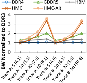
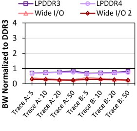
We conclude that SoC accelerators benefit significantly from high-bandwidth memories (e.g., HMC, GDDR5), but the diverse behavior of the different types of accelerators (e.g., multimedia vs. network) makes it difficult to identify a single DRAM type that performs best across the board.
8.3. GPGPU Application Performance
We study ten applications from the Mars (he.pact08, ), Rodinia (rodinia, ), and LonestarGPU (lonestar, ) suites. These applications have diverse memory intensities, with last-level cache MPKIs ranging from 0.005 (dmr) to 25.3 (sp). Figure 20 shows the performance of the applications.
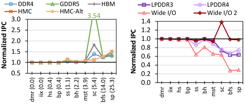
We draw out two key findings from the figure. First, we find that for our applications that are not memory intensive (MPKI 1 for GPGPU applications), all of our DRAM types perform near identically. Second, six of our applications (ss, bh, mst, sc, bfs, sp) are memory intensive, and benefit significantly from executing on a system with high-bandwidth DRAM types (i.e., GDDR5, HBM, or HMC). On average, the IPC of memory-intensive GPGPU applications is 39.7% higher with GDDR5, 26.9% higher with HBM, and 18.3% higher with both HMC and HMC-Alt, compared to DDR3. Unlike the other applications we study, the memory-intensive GPGPU applications also see significant performance improvements with DDR4, which provides an average performance improvement of 16.4% over DDR3.
A large reason for the high speedups of the memory-intensive GPGPU workloads with high-bandwidth DRAM types is memory coalescing (bakhoda.ispass09, ; chatterjee.sc14, ). In a GPU, the memory controller coalesces (i.e., combines) multiple memory requests that target nearby locations in memory into a single memory request. This is particularly useful for GPU and GPGPU applications, where a large number of threads operate in lockstep, and often operate on neighboring pieces of data. Memory coalescing exploits the spatial locality between multiple threads, in order to reduce pressure on the memory system and reduce queuing delays. The coalesced memory requests take significant advantage of the high bandwidth available in GDDR5, and the additional bank parallelism available in DDR4. Coalescing is particularly helpful for sc, where the memory requests are highly bound by the available memory bandwidth (kloosterman.micro15, ). This leads to very high speedups on GDDR5 (253.6%) for sc over DDR3.
Unlike the other memory-intensive applications, memory requests from sp are typically not coalesced (chatterjee.sc14, ) (i.e., requests from multiple threads cannot be combined easily to exploit locality). Without coalescing, the application issues many requests at once to DRAM, and, thus, performs best when it is run on a DRAM type that can provide both high bandwidth and high bank parallelism to service many requests concurrently, such as HBM or HMC. As a result, for sp, HBM outperforms GDDR5 by 8.3%, and HMC outperforms GDDR5 by 11.3%. HMC and HMC-Alt perform within 0.2% of each other, as sp does not have significant locality for HMC-Alt to exploit for additional performance benefits.
We conclude that for memory-intensive GPGPU applications, GDDR5 provides significant performance improvements as long as memory requests can be coalesced, while HBM and HMC improve performance even more when memory requests are not coalesced because both of these DRAM types provide high bank parallelism.
8.4. DRAM Energy Consumption
that have high memory throughput requirements,
GDDR5 provides much greater energy efficiency
(i.e., large performance gains with a
small energy increase) than DDR3.
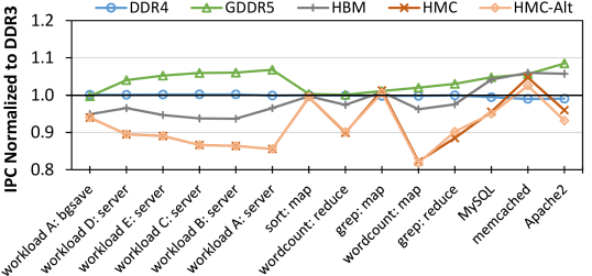
Figure 21 shows the normalized energy consumption for the three major types of heterogeneous system workloads that we study: (1) multimedia acceleration, (2) network acceleration, and (3) GPGPU applications, averaged across all applications of each type. Overall, for multimedia acceleration and GPGPU applications, we observe that GDDR5 consumes more than double the energy of the other memory types, while for network acceleration, GDDR5 consumes only 24.8% more energy than DDR3.
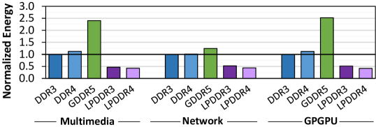
Upon closer inspection, however, we find that for the set of heterogeneous system applications that require high memory throughput (H.264 decoding, all of our network acceleration traces, sc, bfs, and sp), GDDR5’s energy consumption comes with large performance benefits. Figure 22 shows the energy consumption of the high-throughput multimedia and GPGPU applications (see Figure 21 for the network accelerator energy). Averaged across these high-throughput applications, GDDR5 consumes only 31.4% more energy than DDR3, while delivering a performance improvement of 65.6% (not shown). In the extreme case, for sc, GDDR5 consumes only 20.2% more energy than DDR3 to provide a 253.6% speedup. For such accelerator applications, where high memory throughput is combined with high spatial locality, we conclude that GDDR5 can be significantly more energy efficient than the other DRAM types.
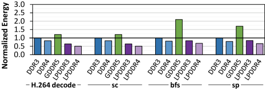
We conclude that certain types of accelerators can achieve higher energy efficiency (i.e., large performance increases with a small energy increase) than with DDR3, by using aggressive DRAM types such as GDDR5, when the accelerators perform tasks that require high memory throughput.
9. Common OS Routines
We collect several traces capturing common kernel-mode activities for different benchmarks:
-
•
IOzone (IOZone, ), a file system benchmark suite that tests a number of I/O performance tasks (Tests 0–12);
-
•
Netperf (Netperf, ), which tests TCP/UDP network calls (UDP_RR, UDP_STREAM, TCP_RR, TCP_STREAM);
-
•
bootup (seshadri.micro13, ), a representative phase of the boot operation in the Debian operating system;
-
•
forkbench (seshadri.micro13, ), a microbenchmark trace that creates a 64MB array of random values, forks itself, and has its child process update 1K random pages; and
-
•
shell (seshadri.micro13, ), a microbenchmark trace of a Unix shell script that runs find on a directory tree and executes ls on each subdirectory.
9.1. Workload Characteristics
While the OS routines that we study perform a variety of different tasks, we find that they exhibit very similar behavior. We depict the row buffer locality of the routines with DDR3 DRAM in Figure 23. From the figure, we find that most of the routines have exceptionally high row buffer locality, with row buffer hit rates greater than 75%. This behavior occurs because many of the OS routines are based on files and file-like structures, and these files are often read or written in large sequential blocks. This causes the routines to access most, if not all, of the data mapped to an OS page (and therefore to the open DRAM row that houses the page). We also observe that memory requests from these routines reach the DRAM at regular time intervals, as opposed to in bursts. The regularly-timed memory requests reduce the peak throughput demand on DRAM.
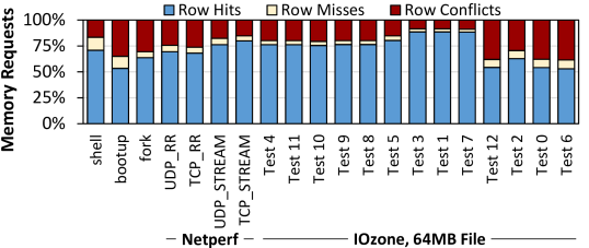
9.2. Performance
Figure 24 shows the performance of the OS routines on standard-power DRAM types, normalized to their performance under DDR3. We find that the overall performance of the routines is similar to the performance trends observed for server and cloud workloads (see Section 7.2): only GDDR5 memory outperforms DDR3 for the majority of routines. The other high-throughput memories are generally unable to significantly improve performance (except HBM, for some workloads), and in many cases actually hurt performance.
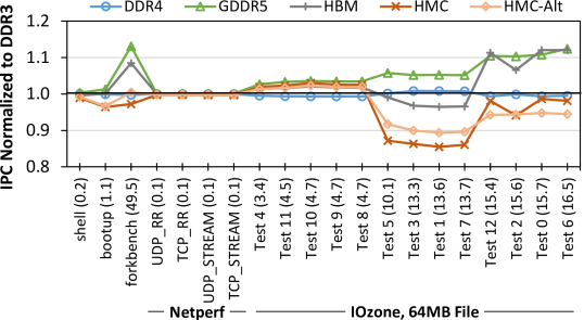
DRAM types with low access latencies
that exploit spatial locality (e.g., GDDR5).
Lower-latency DRAM types such as GDDR5 are best for OS routines due to (1) the serialized access patterns of most of the routines (e.g., dependent memory requests) and (2) the regular time intervals between DRAM requests (see Section 9.1). The regular, serialized accesses require lower latency to be served faster and do not benefit from high memory throughput. As a result, DRAM types that increase access latency to provide higher throughput often hurt the performance of OS routines. This is particularly true of HMC, which greatly sacrifices row buffer locality with its narrow rows to provide high bank parallelism (which OS routines typically cannot take advantage of due to their low BPUs). As we show in Figure 24, if we employ our locality-aware addressing mode for HMC (HMC-Alt), the performance of HMC improves for some (but not all) of the routines, as HMC-Alt can exploit more of the high spatial locality present in OS routines than HMC. GDDR5 provides the highest performance across all OS routines because it reduces latency over DDR3 while also increasing bandwidth.
Figure 25 shows the performance of the common OS routines on low-power DRAM types. We draw out four findings from the figure. First, we observe that the average performance loss from using low-power DRAM types, compared to DDR3, can be relatively small. For example, LPDDR3 leads to an average slowdown of only 6.6% over DDR3. Second, we observe that due to the high sensitivity of OS routines to DRAM access latency, LPDDR4 causes a larger slowdown (9.6% on average over DDR3) than LPDDR3 due to its higher access latency. Third, we observe that there are four routines where Wide I/O 2 provides significant performance improvements over DDR3: Test 12, Test 2, Test 0, and Test 6. This is because Wide I/O 2 significantly increases the row hit rate. As Figure 23 shows, these four routines have much lower row hit rates (an average of 56.1%) than the other routines in DDR3. This is because the four routines have access patterns that lead to a large number of row conflicts. Specifically, Test 12 reads data from a file and scatters it into multiple buffers using the preadv() system call, while Test 2, Test 0, and Test 6 are dominated by write system calls that update both the data and any associated metadata. The data and associated metadata often reside in different parts of the memory address space, which leads to row conflicts in many DRAM types. Wide I/O 2 reduces these row conflicts, and the average row hit rate for these four routines increases to 91.0% (not shown). Fourth, we observe that the performance reduction that forkbench experiences on low-power DRAM types versus DDR3 is much larger than the reduction other routines experience. This is due to the fact that forkbench is significantly more memory intensive (with an MPKI of 49.5) than the other OS routines.
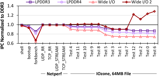
We conclude that OS routines perform better on memories that (1) provide low-latency access and (2) exploit the high amount of spatial locality that exists in the memory access patterns of these routines.
9.3. DRAM Energy Consumption
Figure 26 shows the energy consumed by each of the DRAM types that we have accurate power models for, normalized to DDR3 energy consumption, and averaged across all of the OS routines. We find that the DRAM energy consumption trends of the OS routines is very similar to the trends that we observed for desktop workloads in Section 5.4. Without a large improvement in average performance, GDDR5 consumes 2.1x more energy than DDR3, while LPDDR3/LPDDR4 consume 52.6%/58.0% less energy than DDR3.
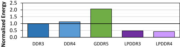
LPDDR3/LPDDR4 incur a much smaller average performance loss (6.6%/9.6%; see Section 9.2) over DDR3 for OS routines than for desktop and scientific applications. While both the OS routines and our desktop and scientific applications exhibit high row buffer locality and low memory intensity, the average row buffer locality is higher for the OS routines, while the average memory intensity is lower. As a result, LPDDR3 and LPDDR4 strike a better compromise between performance and energy consumption for OS routines than they do for desktop and scientific applications.
We conclude that OS routines can attain high energy efficiency (i.e., large energy reductions with a small performance impact), compared to DDR3, when run on low-power DRAM types that provide large row sizes to exploit spatial locality (e.g., LPDDRx).
10. Key Takeaways
From our detailed characterization, and from the twelve key observations that we make, we find that there are a number of high-level lessons and takeaways that can be of use for future DRAM architects, system architects, and programmers. We discuss the four most important (as we deem) takeaways here.
-
(1)
DRAM latency remains a critical bottleneck for many applications. For many of our applications, we observe that the overall application performance degrades when the DRAM access latency increases. These applications cannot easily take advantage of greater memory-level parallelism or higher memory throughput, often because the memory intensity of the applications is not high enough to take advantage of the maximum bandwidth offered by DDR3. As a result, even though many new DRAM types offer higher bandwidth and higher bank parallelism than DDR3, they do not significantly improve performance. In fact, in many cases, new DRAM types reduce performance, because the increased bandwidth and bank parallelism they provide come at the cost of higher latency.
For DRAM architects, this means that newer DRAM types require ways to bring down the latency of a single access, which goes against the recent trend of increasing latency in order to provide other benefits. Several recent works propose ways of reducing DRAM latency at low cost (lee.hpca13, ; kim.isca12, ; lee.hpca15, ; chang.sigmetrics16, ; hassan.hpca16, ; hassan.isca19, ; lee.sigmetrics17, ; kim.iccd18, ; chang.hpca16, ; zhang.hpca16, ; wang.micro18, ; choi.isca15, ; seshadri.micro13, ; chandrasekar.date14, ). We believe such approaches are very promising and critical for modern and future applications, and we encourage the development of more such novel latency reduction mechanisms for DRAM.
For system architects, there is a need to reconsider whether systems should be built with older, lower-latency DRAM types such as DDR3 and GDDR5 instead of with newer, higher-throughput DRAM types such as DDR4 and HMC. The use of memory controller mechanisms to reduce DRAM latency is also promising (lee.hpca15, ; chang.sigmetrics16, ; hassan.hpca16, ; lee.sigmetrics17, ; kim.iccd18, ; zhang.hpca16, ; wang.micro18, ; chandrasekar.date14, ). -
(2)
Bank parallelism is not fully utilized by a wide variety of our applications. As we show in our characterization, bank parallelism utilization (BPU; see Section 4) is a key indicator of whether applications benefit from high-throughput and highly-parallel DRAM types such as HBM and HMC. BPU expresses a combination of the memory intensity and the memory-level parallelism of an application. While there are some applications (e.g., multiprogrammed workloads, high-memory-intensity GPGPU applications) that have high BPU and benefit from using DRAM types such as HBM and HMC, a variety of our applications have low BPU (e.g., single-thread desktop/scientific applications, irregular memory-sensitive multithreaded applications, and server/cloud applications), and thus do not experience appreciable performance gains with HBM and HMC.
For DRAM architects, this indicates that providing a greater number of banks in newer DRAM types may not provide significant gains for especially single-thread performance. For example, while DDR4 doubles the number of banks over DDR3, the increased bank count requires architectural changes (e.g., the introduction of bank groups; see Section 2.2 and Appendix A) that increase access latency. An important (critical) thread with low BPU may not be able to overcome the latency increase, and thus the additional banks would not benefit performance. We see this behavior in several of our workloads, and thus their performance degrades when DDR4 is used instead of DDR3.
For system architects, it may be useful to consider using cheaper DRAM types with fewer banks (and also low latencies) in systems that run applications with low BPU.
We do note that there are several cases where row conflicts remain high even when BPU is low (e.g., our example YCSB server workload in Figure 15, irregular memory-intensive multithreaded workloads, cactusADM, omnetpp, and GemsFDTD). This can occur if memory requests are unevenly distributed across the memory banks, causing some of the banks to be highly contended for while other banks remain idle. For both DRAM architects and programmers, this indicates that there are opportunities to change address interleavings, memory schedulers, memory allocation, and program access patterns to make better use of the available bank-level parallelism. -
(3)
Spatial locality continues to provide significant performance benefits if it is exploited by the memory subsystem. One of the more significant changes made in HMC versus other DRAM types is the reduction of the row buffer size. A row in HMC () is 97% smaller than a row in DDR3/DDR4 (). HMC uses the shorter row size to significantly increase bank-level parallelism and memory throughput. Due to the limited BPU of many applications, the increased parallelism and throughput only occasionally provide benefits when using HMC. In contrast to bank parallelism, applications and virtual memory managers still try to maximize spatial locality as much as they can. While most DRAM types exploit this spatial locality (by using large rows to amortize the high penalty of a row conflict), HMC’s small rows are unable to effectively capture much of this locality. As a result, HMC provides notable performance improvements only in cases where spatial locality is low (or is destroyed), such as for highly-memory-intensive multiprogrammed workloads where multiple applications significantly interfere with each other. Otherwise, HMC can lead to large performance losses compared to other high-throughput memories (e.g., GDDR5, HBM), and HMC often performs worse than most other DRAM types.
For DRAM architects, our observations indicate that new DRAM types that activate at a row granularity should not reduce the row width. A reduced row width typically requires more row activation operations for the same amount of data, which introduces a significant overhead that cannot be (easily) amortized by other benefits (such as higher memory-level parallelism in HMC).
For programmers, applications should maximize the amount of spatial locality that they exploit, as most DRAM types are designed to perform better with higher locality. This could require (a) redesigning data structures to maximize spatial locality based on the application’s memory access patterns, and (b) issuing fewer, larger memory allocation requests that the virtual memory manager can attempt to allocate contiguously in the physical address space. Alternatively, for programs that will execute on systems that make use of low-spatial-locality memories such as HMC, programmers should take the poor hardware locality into account and perhaps rewrite their applications to take better advantage of the large available bank-level parallelism. -
(4)
For some classes of applications, low-power memory can provide large energy savings without sacrificing significant performance. In particular, if we compare DDR3 with LPDDR4, we find that there are two types of memory behavior where LPDDR4 significantly reduces DRAM energy consumption without a significant performance overhead. First, applications with low memory intensity do not perform a large number of memory accesses. As a result, despite the much higher access latency of LPDDR4 ( for a row miss) over that of DDR3 (), such applications do not experience a significant impact on their overall execution time. Second, applications with high BPU can take advantage of the larger number of banks in LPDDR4. The greater number of banks in LPDDR4 (16 per rank) than in DDR3 (8 per rank) actually helps LPDDR4 to (partially) overcome the overhead of additional latency.
For system architects, this means that there are a number of cases where they can deploy systems that use LPDDR4 to reduce the system energy consumption with a small impact on system performance, thereby improving energy efficiency.
For DRAM architects, there is a need to develop new DRAM types and subsystems that consume low energy without impacting system performance across a broad range of applications.
11. Related Work
To our knowledge, this is (1) the first work to uncover new trends about and interactions between different DRAM types and the performance and energy consumption of modern workloads, (2) the most extensive study performed to date on the combined DRAM–workload behavior, and (3) the most comprehensive study to date that compares the performance of monolithic (i.e., 2D) and 3D-stacked DRAM. No prior work presents a comprehensive study across such a wide variety of workloads (115 of them) and DRAM types (nine of them). We briefly discuss the most closely related works.
Cuppu et al. (cuppu.isca99, ; cuppu.tc01, ) present a study of seven DRAM types and their interaction with a suite of desktop and scientific applications. Their work, more than two decades old now, noted several characteristics emerging from then-contemporary DRAM designs (many of which do not exist in the field today), and made recommendations based on these insights. Similar to some of our findings, Cuppu et al. recommend that memory latency needs to be reduced, and spatial locality needs to be further exploited by the memory subsystem. Other recommendations from Cuppu et al. are more relevant for the older DRAM types that they study, and in some cases do not apply to the modern DRAM types that we study in this work. Later work by Cuppu and Jacob (cuppu.isca01, ) studies the impact of different memory channel configurations on application performance, which is orthogonal to the characterizations that we perform.
Zhu and Zhang (zhu.hpca05, ) study how various DRAM types can be optimized to work with simultaneous multithreading (SMT) processors, but do not perform a broad characterization of applications. Zheng and Zhu (zheng.tc10, ) compare the performance of DDR3 DRAM to DDR2 (ddr2, ) and FB-DIMM (fbdimm, ) for 26 desktop and scientific applications. Gomony et al. (gomony.date12, ) characterize three low-power DRAM types for mobile systems, and propose a tool to select the right type for real-time mobile systems. All of these studies predate the emergence of most of the DRAM types that we characterize (DDR4, LPDDR3, LPDDR4, HBM, HMC, Wide I/O 2), do not evaluate energy consumption, and focus only on a limited set of applications.
Li et al. (li.memsys18, ) evaluate the performance and power of nine modern DRAM types, including two versions each of HMC and HBM. However, unlike our wide range of applications, their evaluation studies only 10 desktop and scientific applications. Furthermore, their memory configuration uses row interleaving, which reduces the bank-level parallelism compared to many modern systems that use cache line interleaving (kim.isca12, ; jeong.hpca12, ; kim.hpca10, ; coregen7.datasheet, ; xeone5.datasheet, ; lenovo.xeon.memconfig, ; power9.datasheet, ; zhang.micro00, ; rokicki.tr96, ).
Several works study the impact of new and existing memory controller policies on performance (e.g., (rixner.isca00, ; kim.micro10, ; ghose.isca13, ; ipek.isca08, ; mutlu.isca08, ; kim.hpca10, ; kaseridis.micro2011, ; subramanian.iccd14, ; mutlu.micro07, ; usui.taco16, ; hur.micro04, ; nesbit.micro06, ; mukundan.hpca12, ; subramanian.tpds16, ; moscibroda.podc08, ; ausavarungnirun.isca12, ; muralidhara.micro11, ; rixner.micro04, ; ebrahimi.micro11, ; yuan.micro09, ; jeong.dac12, ; liu.isca12, ; venkatesan.hpca06, ; isen.micro09, ; lee.tr10, ; zhang.micro00, ; rokicki.tr96, ; lee.pact15, ; chang.hpca14, ; lee.hpca15, ; chang.sigmetrics16, ; hassan.hpca16, ; lee.sigmetrics17, ; kim.iccd18, ; zhang.hpca16, ; wang.micro18, ; lee.micro09, ; lee.micro08, ; ebrahimi.isca11, ; seshadri.isca14, ; zhao.micro14, ; jog.sigmetrics16, ; das.dac18, ; stuecheli.isca10, ; stuecheli.micro10, ; chandrasekar.date14, )). These works are orthogonal to our study, which keeps controller policies constant and explores the effect of the underlying DRAM type. Other works profile the low-level behavior of DRAM types by characterizing real DRAM chips (e.g., (lee.hpca15, ; chang.sigmetrics16, ; lee.sigmetrics17, ; ghose.sigmetrics18, ; chang.sigmetrics17, ; kim.isca14, ; kim.hpca19, ; liu.isca13, ; patel.dsn19, ; kim.hpca18, ; kim.iccd18, ; khan.dsn16, ; qureshi.dsn15, ; patel.isca17, ; khan.sigmetrics14, ; khan.micro17, ; khan.cal16, ; hassan.hpca17, ; chandrasekar.date14, )). These works focus on a single DRAM type (DDR3 or LPDDR4), and do not use real-world applications to perform their characterization, since their goal is to understand device behavior independently of workloads. A few works (meza.dsn15, ; schroeder.sigmetrics09, ; hwang.asplos12, ; sridharan.sc13, ; sridharan.asplos15, ) perform large-scale characterization studies of DRAM errors in the field. These works examine reliability in a specific setting (e.g., datacenters, supercomputers), and as a result they do not focus on metrics such as performance or energy, and do not consider a broad range of application domains.
A number of works study the memory access behavior of benchmark suites (e.g., (parsec, ; henning.computer00, ; he.pact08, ; singh.icpe19, ; murphy.tc07, ; agaram.ismm06, ; charney.ibmjrd97, ; mccalpin.tcca95, )). These works focus on only a single DRAM type. Conversely, several works propose DRAM simulators and use the simulators to study the memory access behavior of a limited set of workloads on several memory types (kim.cal15, ; rosenfeld-cal2011, ; radulovic.memsys15, ; suresh.cluster14, ; giridhar.sc13, ; ahn.sc09, ; li.sc17, ). None of these studies (1) take a comprehensive look at as wide a range of workloads and DRAM types as we do, or (2) evaluate energy consumption.
12. Conclusion
It has become very difficult to intuitively understand how modern applications interact with different DRAM types. This is due to the emergence of (1) many new DRAM types, each catering to different needs (e.g., high bandwidth, low power, high memory density); and (2) new applications that are often data intensive. The combined behavior of each pair of workload and DRAM type is impacted by the complex interaction between memory latency, bandwidth, bank parallelism, row buffer locality, memory access patterns, and energy consumption. In this work, we perform a comprehensive experimental study to analyze these interactions, by characterizing the behavior of 115 applications and workloads across nine DRAM types. With the help of new metrics that capture the interaction between memory access patterns and the underlying hardware, we make 12 key observations and draw out many new findings about the combined DRAM–workload behavior. We then provide a number of recommendations for DRAM architects, system architects, and programmers. We hope that our observations inspire the development of many memory optimizations in both hardware and software. To this end, we have released our toolchain with the hope that the tools can assist with future studies and research on memory optimization in both hardware and software.
Acknowledgments
We thank our shepherd Evgenia Smirni and the anonymous reviewers for feedback. We thank the SAFARI Research Group members for feedback and the stimulating intellectual environment they provide. We acknowledge the generous support of our industrial partners: Alibaba, Facebook, Google, Huawei, Intel, Microsoft, and VMware. This research was supported in part by the Semiconductor Research Corporation and the National Science Foundation.
References
- (1) Advanced Micro Devices, Inc., “High Bandwidth Memory (HBM) DRAM,” 2013.
- (2) K. K. Agaram, S. W. Keckler, C. Lin, and K. S. McKinley, “Decomposing Memory Performance: Data Structures and Phases,” in ISMM, 2006.
- (3) J. Ahn, N. Jouppi, C. Kozyrakis, J. Leverich, and R. Schreiber, “Future Scaling of Processor-Memory Interfaces,” in SC, 2009.
- (4) M. A. Z. Alves, C. Villavieja, M. Diener, F. B. Moreira, and P. O. A. Navaux, “SiNUCA: A Validated Micro-Architecture Simulator,” in HPCC/CSS/ICESS, 2015.
- (5) Apache Foundation, “Apache Hadoop,” http://hadoop.apache.org/.
- (6) Apache Foundation, “Apache HTTP Server Project,” http://www.apache.org/.
- (7) R. Ausavarungnirun, K. K. Chang, L. Subramanian, G. H. Loh, and O. Mutlu, “Staged Memory Scheduling: Achieving High Performance and Scalability in Heterogeneous Systems,” in ISCA, 2012.
- (8) A. Bakhoda, G. Yuan, W. W. L. Fung, H. Wong, and T. M. Aamodt, “Analyzing CUDA Workloads Using a Detailed GPU Simulator,” in ISPASS, 2009.
- (9) P. Balaprakash, D. Buntinas, A. Chan, A. Guha, R. Gupta, S. H. K. Narayanan, A. A. Chien, P. Hovland, and B. Norris, “Exascale Workload Characterization and Architecture Implications,” in ISPASS, 2013.
- (10) C. Bienia, S. Kumar, J. P. Singh, and K. Li, “The PARSEC Benchmark Suite: Characterization and Architectural Implications,” Princeton Univ. Dept. of Computer Science, Tech. Rep. TR-811-08, 2008.
- (11) N. Binkert, B. Beckmann, G. Black, S. K. Reinhardt, A. Saidi, A. Basu, J. Hestness, D. R. Hower, T. Krishna, S. Sardashti, R. Sen, K. Sewell, M. Shoaib, N. Vaish, M. D. Hill, and D. A. Wood, “gem5: A Multiple-ISA Full System Simulator with Detailed Memory Model,” CAN, 2011.
- (12) M. Burtscher, R. Nasre, and K. Pingali, “A Quantitative Study of Irregular Programs on GPUs,” in IISWC, 2012.
- (13) Canonical Ltd., “Ubuntu 14.04 LTS (Trusty Tahr),” http://releases.ubuntu.com/14.04/, 2014.
- (14) Canonical Ltd., “Ubuntu 16.04 LTS (Xenial Xerus),” http://releases.ubuntu.com/16.04/, 2016.
- (15) K. Chandrasekar, S. Goossens, C. Weis, M. Koedam, B. Akesson, N. Wehn, and K. Goossens, “Exploiting Expendable Process-Margins in DRAMs for Run-Time Performance Optimization,” in DATE, 2014.
- (16) K. Chandrasekar, C. Weis, Y. Li, S. Goossens, M. Jung, O. Naji, B. Akesson, N. Wehn, and K. Goossens, “DRAMPower: Open-Source DRAM Power & Energy Estimation Tool,” http://www.drampower.info.
- (17) K. K. Chang, D. Lee, Z. Chishti, A. Alameldeen, C. Wilkerson, Y. Kim, and O. Mutlu, “Improving DRAM Performance by Parallelizing Refreshes With Accesses,” in HPCA, 2014.
- (18) K. K. Chang, P. J. Nair, S. Ghose, D. Lee, M. K. Qureshi, and O. Mutlu, “Low-Cost Inter-Linked Subarrays (LISA): Enabling Fast Inter-Subarray Data Movement in DRAM,” in HPCA, 2016.
- (19) K. K. Chang, A. G. Yağlıkçı, S. Ghose, A. Agrawal, N. Chatterjee, A. Kashyap, D. Lee, M. O’Connor, H. Hassan, and O. Mutlu, “Understanding Reduced-Voltage Operation in Modern DRAM Devices: Experimental Characterization, Analysis, and Mechanisms,” in SIGMETRICS, 2017.
- (20) K. K. Chang, “Understanding and Improving the Latency of DRAM-Based Memory Systems,” Ph.D. dissertation, Carnegie Mellon Univ., 2017.
- (21) K. K. Chang, A. Kashyap, H. Hassan, S. Ghose, K. Hsieh, D. Lee, T. Li, G. Pekhimenko, S. Khan, and O. Mutlu, “Understanding Latency Variation in Modern DRAM Chips: Experimental Characterization, Analysis, and Optimization,” in SIGMETRICS, 2016.
- (22) M. J. Charney and T. R. Puzak, “Prefetching and Memory System Behavior of the SPEC95 Benchmark Suite,” IBM JRD, 1997.
- (23) N. Chatterjee, M. O’Connor, G. H. Loh, N. Jayasena, and R. Balasubramonian, “Managing DRAM Latency Divergence in Irregular GPGPU Applications,” in SC, 2014.
- (24) S. Che, M. Boyer, J. Meng, D. Tarjan, J. Sheaffer, S.-H. Lee, and K. Skadron, “Rodinia: A Benchmark Suite for Heterogeneous Computing,” in IISWC, 2009.
- (25) J. Choi, W. Shin, J. Jang, J. Suh, Y. Kwon, Y. Moon, and L.-S. Kim, “Multiple Clone Row DRAM: A Low Latency and Area Optimized DRAM,” in ISCA, 2015.
- (26) Y. Chou, B. Fahs, and S. Abraham, “Microarchitecture Optimizations for Exploiting Memory-Level Parallelism,” in ISCA, 2004.
- (27) B. F. Cooper, A. Silberstein, E. Tam, R. Ramakrishnan, and R. Sears, “Benchmarking Cloud Serving Systems with YCSB,” in SoCC, 2010.
- (28) V. Cuppu, B. Jacob, B. Davis, and T. Mudge, “A Performance Comparison of Contemporary DRAM Architectures,” in ISCA, 1999.
- (29) V. Cuppu, B. Jacob, B. Davis, and T. Mudge, “High-Performance DRAMs in Workstation Environments,” in IEEE Transactions on Computers, 2001.
- (30) V. Cuppu and B. Jacob, “Concurrency, Latency, or System Overhead: Which Has the Largest Impact on Uniprocessor DRAM-System Performance?” in ISCA, 2001.
- (31) A. Das, H. Hassan, and O. Mutlu, “VRL-DRAM: Improving DRAM Performance via Variable Refresh Latency,” in DAC, 2018.
- (32) R. Das, O. Mutlu, T. Moscibroda, and C. Das, “Application-Aware Prioritization Mechanisms for On-Chip Networks,” in MICRO, 2009.
- (33) H. David, C. Fallin, E. Gorbatov, U. R. Hanebutte, and O. Mutlu, “Memory Power Management via Dynamic Voltage/Frequency Scaling,” in ICAC, 2011.
- (34) J. Dean and S. Ghemawat, “MapReduce: Simplified Data Processing on Large Clusters,” in OSDI, 2004.
- (35) R. Desikan, D. Burger, and S. W. Keckler, “Measuring Experimental Error in Microprocessor Simulation,” in ISCA, 2001.
- (36) D. E. Difallah, A. Pavlo, C. Curino, and P. Cudre-Mauroux, “OLTP-Bench: An Extensible Testbed for Benchmarking Relational Databases,” in VLDB, 2004.
- (37) X. Dong, C. Xu, Y. Xie, and N. P. Jouppi, “NVSim: A Circuit-Level Performance, Energy, and Area Model for Emerging Nonvolatile Memory,” TCAD, 2012.
- (38) Dormando, “Memcached: High-Performance Distributed Memory Object Caching System,” http://memcached.org/.
- (39) E. Ebrahimi, C. J. Lee, O. Mutlu, and Y. N. Patt, “Prefetch-Aware Shared Resource Management for Multi-Core Systems,” in ISCA, 2011.
- (40) E. Ebrahimi, R. Miftakhutdinov, C. Fallin, C. J. Lee, J. A. Joao, O. Mutlu, and Y. N. Patt, “Parallel application memory scheduling,” in MICRO, 2011.
- (41) F. A. Endo, D. Coroussé, and H.-P. Charles, “Micro-Architectural Simulation of In-Order and Out-of-Order ARM Microprocessors with gem5,” in SAMOS, 2014.
- (42) S. Eyerman and L. Eeckhout, “System-Level Performance Metrics for Multiprogram Workloads,” IEEE Micro, 2008.
- (43) J. Fritts and B. Mangione-Smith, “MediaBench II - Technology, Status, and Cooperation,” in The Workshop on Media and Stream Processors, 2002.
- (44) S. Ghose, H. Lee, and J. F. Martínez, “Improving Memory Scheduling via Processor-Side Load Criticality Information,” in ISCA, 2013.
- (45) S. Ghose, A. G. Yağlıkçı, R. Gupta, D. Lee, K. Kudrolli, W. X. Liu, H. Hassan, K. K. Chang, N. Chatterjee, A. Agrawal, M. O’Connor, and O. Mutlu, “What Your DRAM Power Models Are Not Telling You: Lessons from a Detailed Experimental Study,” in SIGMETRICS, 2018.
- (46) B. Giridhar, M. Cieslak, D. Duggal, R. Dreslinski, H. Chen, R. Patti, B. Hold, C. Chakrabarti, T. Mudge, and D. Blaauw, “Exploring DRAM Organizations for Energy-Efficient and Resilient Exascale Memories,” in SC, 2013.
- (47) A. Glew, “MLP Yes! ILP No! Memory Level Parallelism, or Why I No Longer Care About Instruction Level Parallelism,” in ASPLOS WACI, 1998.
- (48) M. D. Gomony, C. Weis, B. Akesson, N. Wehn, and K. Goossens, “DRAM Selection and Configuration for Real-Time Mobile Systems,” in DATE, 2012.
- (49) G. Hamerly, E. Perelman, J. Lau, and B. Calder, “Simpoint 3.0: Faster and More Flexible Program Phase Analysis,” JILP, 2005.
- (50) H. Hassan, M. Patel, J. S. Kim, A. G. Yağlıkçı, N. Vijaykumar, N. M. Ghiasi, S. Ghose, and O. Mutlu, “CROW: A Low-Cost Substrate for Improving DRAM Performance, Energy Efficiency, and Reliability,” in ISCA, 2019.
- (51) H. Hassan, N. Vijaykumar, S. Khan, S. Ghose, K. Chang, G. Pekhimenko, D. Lee, O. Ergin, and O. Mutlu, “SoftMC: A Flexible and Practical Open-Source Infrastructure for Enabling Experimental DRAM Studies,” in HPCA, 2017.
- (52) H. Hassan, G. Pekhimenko, N. Vijaykumar, V. Seshadri, D. Lee, O. Ergin, and O. Mutlu, “ChargeCache: Reducing DRAM Latency by Exploiting Row Access Locality,” in HPCA, 2016.
- (53) B. He, W. Fang, Q. Luo, N. Govindaraju, and T. Wang, “Mars: A MapReduce Framework on Graphics Processors,” in PACT, 2008.
- (54) J. L. Henning, “SPEC CPU2000: Measuring CPU Performance in the New Millennium,” IEEE Computer, 2000.
- (55) Hewlett-Packard, “Netperf: A Network Performance Benchmark (Rev. 2.1),” 1996.
- (56) U. Holzle and L. A. Barroso, The Datacenter as a Computer: An Introduction to the Design of Warehouse-Scale Machines. Morgan & Claypool, 2009.
- (57) I. Hur and C. Lin, “Adaptive History-Based Memory Schedulers,” in MICRO, 2004.
- (58) A. Hwang, I. Stefanovici, and B. Schroeder, “Cosmic Rays Don’t Strike Twice: Understanding the Nature of DRAM Errors and the Implications for System Design,” in ASPLOS, 2012.
- (59) Hybrid Memory Cube Consortium, “Hybrid Memory Cube Specification 2.1,” 2015.
- (60) IBM Corp., POWER9 Processor RegistersSpecification, Vol. 3, May 2017.
- (61) Intel Corp., “Product Specification: Intel® Core™ i7-2600K,” https://ark.intel.com/products/52214/.
- (62) Intel Corp., “Product Specification: Intel® Core™ i7-975 Processor Extreme Edition,” https://ark.intel.com/products/37153/.
- (63) Intel Corp., “Product Specification: Intel® Xeon® Processor E5-2630 v4,” https://ark.intel.com/products/92981/.
- (64) Intel Corp., 7th Generation Intel® Processor Families for S Platforms and Intel® Core™ X-Series Processor Family Datasheet, Vol. 1, December 2018.
- (65) Intel Corp., Intel® Xeon® Processor E5-1600/2400/2600/4600 (E5-Product Family) Product Families Datasheet Vol. 2, May 2018.
- (66) IOzone Lab, “IOzone Filesystem Benchmark,” http://www.iozone.org/, 2016.
- (67) E. İpek, O. Mutlu, J. F. Martínez, and R. Caruana, “Self-Optimizing Memory Controllers: A Reinforcement Learning Approach,” in ISCA, 2008.
- (68) C. Isen and L. John, “ESKIMO — Energy Savings Using Semantic Knowledge of Inconsequential Memory Occupancy for DRAM Subsystem,” in MICRO, 2009.
- (69) J. Jeddeloh and B. Keeth, “Hybrid Memory Cube New DRAM Architecture Increases Density and Performance,” in VLSIT, 2012.
- (70) JEDEC Solid State Technology Assn., JESD206: FBDIMM Architecture and Protocol, January 2007.
- (71) JEDEC Solid State Technology Assn., JESD79-2F: DDR2 SDRAM Standard, November 2009.
- (72) JEDEC Solid State Technology Assn., JESD229: Wide I/O Single Data Rate (Wide I/O SDR) Standard, December 2011.
- (73) JEDEC Solid State Technology Assn., JESD79-3F: DDR3 SDRAM Standard, July 2012.
- (74) JEDEC Solid State Technology Assn., JESD235: High Bandwidth Memory (HBM) DRAM, October 2013.
- (75) JEDEC Solid State Technology Assn., JESD229-2: Wide I/O 2 (WideIO2) Standard, August 2014.
- (76) JEDEC Solid State Technology Assn., JESD209-3C: Low Power Double Data Rate 3 (LPDDR3) Standard, August 2015.
- (77) JEDEC Solid State Technology Assn., JESD212C: Graphics Double Data Rate (GDDR5) SGRAM Standard, February 2016.
- (78) JEDEC Solid State Technology Assn., JESD209-4B: Low Power Double Data Rate 4 (LPDDR4) Standard, March 2017.
- (79) JEDEC Solid State Technology Assn., JESD79-4B: DDR4 SDRAM Standard, June 2017.
- (80) M. K. Jeong, D. H. Yoon, D. Sunwoo, M. Sullivan, I. Lee, and M. Erez, “Balancing DRAM Locality and Parallelism in Shared Memory CMP Systems,” in HPCA, 2012.
- (81) M. K. Jeong, M. Erez, C. Sudanthi, and N. Paver, “A QoS-Aware Memory Controller for Dynamically Balancing GPU and CPU Bandwidth Use in an MPSoC,” in DAC, 2012.
- (82) A. Jog, O. Kayiran, A. Pattnaik, M. T. Kandemir, O. Mutlu, R. Iyer, and C. R. Das, “Exploiting Core Criticality for Enhanced GPU Performance,” in SIGMETRICS, 2016.
- (83) U. Kang, H.-S. Yu, C. Park, H. Zheng, J. Halbert, K. Bains, S. Jang, and J. Choi, “Co-Architecting Controllers and DRAM to Enhance DRAM Process Scaling,” in The Memory Forum, 2014.
- (84) D. Kaseridis, J. Stuecheli, and L. K. John, “Minimalist Open-Page: A DRAM Page-Mode Scheduling Policy for the Many-Core Era,” in MICRO, 2011.
- (85) S. Khan, D. Lee, and O. Mutlu, “PARBOR: An Efficient System-Level Technique to Detect Data Dependent Failures in DRAM,” in DSN, 2016.
- (86) S. Khan, D. Lee, Y. Kim, A. R. Alameldeen, C. Wilkerson, and O. Mutlu, “The Efficacy of Error Mitigation Techniques for DRAM Retention Failures: A Comparative Experimental Study,” in SIGMETRICS, 2014.
- (87) S. Khan, C. Wilkerson, D. Lee, A. R. Alameldeen, and O. Mutlu, “A Case for Memory Content-Based Detection and Mitigation of Data-Dependent Failures in DRAM,” CAL, 2016.
- (88) S. Khan, C. Wilkerson, Z. Wang, A. Alameldeen, D. Lee, and O. Mutlu, “Detecting and Mitigating Data-Dependent DRAM Failures by Exploiting Current Memory Content,” in MICRO, 2017.
- (89) G. Kim, J. Kim, J. H. Ahn, and J. Kim, “Memory-Centric System Interconnect Design with Hybrid Memory Cubes,” in PACT, 2013.
- (90) J. S. Kim, C. Oh, H. Lee, D. Lee, H. R. Hwang, S. Hwang, B. Na, J. Moon, J. G. Kim, H. Park, J. W. Ryu, K. Park, S. K. Kang, S. Y. Kim, H. Kim, J. M. Bang, H. Cho, M. Jang, C. Han, J. B. Lee, K. Kyung, J. S. Choi, and Y. H. Jun, “A 1.2V 12.8GB/s 2Gb Mobile Wide-I/O DRAM with 4x128 I/Os Using TSV-Based Stacking,” in ISSCC, 2011.
- (91) J. S. Kim, M. Patel, H. Hassan, and O. Mutlu, “Solar-DRAM: Reducing DRAM Access Latency by Exploiting the Variation in Local Bitlines,” in ICCD, 2018.
- (92) J. S. Kim, M. Patel, H. Hassan, and O. Mutlu, “The DRAM Latency PUF: Quickly Evaluating Physical Unclonable Functions by Exploiting the Latency–Reliability Tradeoff in Modern DRAM Devices,” in HPCA, 2018.
- (93) J. S. Kim, M. Patel, H. Hassan, L. Orosa, and O. Mutlu, “D-RaNGe: Using Commodity DRAM Devices to Generate True Random Numbers with Low Latency and High Throughput,” in HPCA, 2019.
- (94) Y. Kim, D. Han, O. Mutlu, and M. Harchol-Balter, “ATLAS: A Scalable and High-Performance Scheduling Algorithm for Multiple Memory Controllers,” in HPCA, 2010.
- (95) Y. Kim, M. Papamichael, O. Mutlu, and M. Harchol-Balter, “Thread Cluster Memory Scheduling: Exploiting Differences in Memory Access Behavior,” in MICRO, 2010.
- (96) Y. Kim, W. Yang, and O. Mutlu, “Ramulator: A Fast and Extensible DRAM Simulator,” CAL, 2015.
- (97) Y. Kim, R. Daly, J. Kim, C. Fallin, J. H. Lee, D. Lee, C. Wilkerson, K. Lai, and O. Mutlu, “Flipping Bits in Memory Without Accessing Them: An Experimental Study of DRAM Disturbance Errors,” in ISCA, 2014.
- (98) Y. Kim, V. Seshadri, D. Lee, J. Liu, and O. Mutlu, “A Case for Exploiting Subarray-Level Parallelism (SALP) in DRAM,” in ISCA, 2012.
- (99) N. Kırman, M. Kırman, M. Chaudhuri, and J. F. Martínez, “Checkpointed Early Load Retirement,” in HPCA, 2005.
- (100) J. Kloosterman, J. Beaumont, M. Wollman, A. Sethia, R. Dreslinski, T. Mudge, and S. Mahlke, “WarpPool: Sharing Requests with Inter-Warp Coalescing for Throughput Processors,” in MICRO, 2015.
- (101) K. Lawton, B. Denney, and C. Bothamy, “The Bochs IA-32 emulator project,” http://bochs.sourceforge.net, 2006.
- (102) C. J. Lee, O. Mutlu, V. Narasiman, and Y. N. Patt, “Prefetch-Aware DRAM Controllers,” in MICRO, 2008.
- (103) C. J. Lee, V. Narasiman, O. Mutlu, and Y. N. Patt, “Improving Memory Bank-Level Parallelism in the Presence of Prefetching,” in MICRO, 2009.
- (104) C. J. Lee, E. Ebrahimi, V. Narasiman, O. Mutlu, and Y. N. Patt, “DRAM-Aware Last-Level Cache Writeback: Reducing Write-Caused Interference in Memory Systems,” Univ. of Texas at Austin, High Performance Systems Group, Tech. Rep. TR-HPS-2010-002, 2010.
- (105) D. Lee, S. Khan, L. Subramanian, S. Ghose, R. Ausavarungnirun, G. Pekhimenko, V. Seshadri, and O. Mutlu, “Design-Induced Latency Variation in Modern DRAM Chips: Characterization, Analysis, and Latency Reduction Mechanisms,” in SIGMETRICS, 2017.
- (106) D. Lee, L. Subramanian, R. Ausavarungnirun, J. Choi, and O. Mutlu, “Decoupled Direct Memory Access: Isolating CPU and IO Traffic by Leveraging a Dual-Data-Port DRAM,” in PACT, 2015.
- (107) D. Lee, “Reducing DRAM Latency at Low Cost by Exploiting Heterogeneity,” Ph.D. dissertation, Carnegie Mellon Univ., 2016.
- (108) D. Lee, S. Ghose, G. Pekhimenko, S. Khan, and O. Mutlu, “Simultaneous Multi-Layer Access: Improving 3D-Stacked Memory Bandwidth at Low Cost,” TACO, 2016.
- (109) D. Lee, Y. Kim, G. Pekhimenko, S. Khan, V. Seshadri, K. Chang, and O. Mutlu, “Adaptive-Latency DRAM: Optimizing DRAM Timing for the Common-Case,” in HPCA, 2015.
- (110) D. Lee, Y. Kim, V. Seshadri, J. Liu, L. Subramanian, and O. Mutlu, “Tiered-Latency DRAM: A Low Latency and Low Cost DRAM Architecture,” in HPCA, 2013.
- (111) C. Lefurgy, K. Rajamani, F. Rawson, W. Felter, M. Kistler, and T. Keller, “Energy Management for Commercial Servers,” Computer, 2003.
- (112) Lenovo Group Ltd., “Intel Xeon Scalable Family Balanced Memory Configurations,” https://lenovopress.com/lp0742.pdf, 2017.
- (113) A. Li, W. Liu, M. R. B. Kistensen, B. Vinter, H. Wang, K. Hou, A. Marquez, and S. L. Song, “Exploring and Analyzing the Real Impact of Modern On-Package Memory on HPC Scientific Kernels,” in SC, 2017.
- (114) S. Li, D. Reddy, and B. Jacob, “A Performance & Power Comparison of Modern High-Speed DRAM Architectures,” in MEMSYS, 2018.
- (115) J. Liu, B. Jaiyen, R. Veras, and O. Mutlu, “RAIDR: Retention-Aware Intelligent DRAM Refresh,” in ISCA, 2012.
- (116) J. Liu, B. Jaiyen, Y. Kim, C. Wilkerson, and O. Mutlu, “An Experimental Study of Data Retention Behavior in Modern DRAM Devices: Implications for Retention Time Profiling Mechanisms,” in ISCA, 2013.
- (117) G. H. Loh, “3D-Stacked Memory Architectures for Multi-Core Processors,” in ISCA, 2008.
- (118) C.-K. Luk, R. Cohn, R. Muth, H. Patil, A. Klauser, G. Lowney, S. Wallace, V. J. Reddi, and K. Hazelwood, “Pin: Building Customized Program Analysis Tools with Dynamic Instrumentation,” in PLDI, 2005.
- (119) K. Luo, J. Gummaraju, and M. Franklin, “Balancing Throughput and Fairness in SMT Processors,” in ISPASS, 2001.
- (120) K. T. Malladi, F. A. Nothaft, K. Periyathambi, B. C. Lee, C. Kozyrakis, and M. Horowitz, “Towards Energy-Proportional Datacenter Memory with Mobile DRAM,” in ISCA, 2012.
- (121) J. A. Mandelman, R. H. Dennard, G. B. Bronner, J. K. DeBrosse, R. Divakaruni, Y. Li, and C. J. Radens, “Challenges and Future Directions for the Scaling of Dynamic Random-Access Memory (DRAM),” IBM JRD, 2002.
- (122) J. D. McCalpin, “Memory Bandwidth and Machine Balance in Current High Performance Computers,” TCCA Newsletter, 1995.
- (123) J. Meza, Q. Wu, S. Kumar, and O. Mutlu, “Revisiting Memory Errors in Large-Scale Production Data Centers: Analysis and Modeling of New Trends from the Field,” in DSN, 2015.
- (124) Micron Technology, Inc., Technical Note TN-46-12: Mobile DRAM Power-Saving Features and Calculations, May 2009, https://www.micron.com/~/media/documents/products/technical-note/dram/tn4612.pdf.
- (125) Micron Technology, Inc., “DDR3 SDRAM Verilog Model, v. 1.74,” https://www.micron.com/-/media/client/global/documents/products/sim-model/dram/ddr3/ddr3-sdram-verilog-model.zip, 2015.
- (126) Micron Technology, Inc., 178-Ball 2E0F Mobile LPDDR3 SDRAM Data Sheet, April 2016.
- (127) Micron Technology, Inc., 2Gb: x4, x8, x16 DDR3 SDRAM Data Sheet, February 2016.
- (128) Micron Technology, Inc., 200-Ball Z01M LPDDR4 SDRAM Automotive Data Sheet, May 2018.
- (129) Micron Technology, Inc., 4Gb: x4, x8, x16 DDR4 SDRAM Data Sheet, June 2018.
- (130) T. Moscibroda and O. Mutlu, “Distributed Order Scheduling and Its Application to Multi-Core DRAM Controllers,” in PODC, 2008.
- (131) J. Mukundan and J. F. Martínez, “MORSE: Multi-objective Reconfigurable Self-Optimizing Memory Scheduler,” in HPCA, 2012.
- (132) S. P. Muralidhara, L. Subramanian, O. Mutlu, M. Kandemir, and T. Moscibroda, “Reducing Memory Interference in Multicore Systems via Application-Aware Memory Channel Partitioning,” in MICRO, 2011.
- (133) R. C. Murphy and P. M. Kogge, “On the Memory Access Patterns of Supercomputer Applications: Benchmark Selection and Its Implications,” TC, 2007.
- (134) O. Mutlu, “The RowHammer Problem and Other Issues We May Face as Memory Becomes Denser,” in DATE, 2017.
- (135) O. Mutlu and T. Moscibroda, “Parallelism-Aware Batch Scheduling: Enhancing Both Performance and Fairness of Shared DRAM Systems,” in ISCA, 2008.
- (136) O. Mutlu, “Memory Scaling: A Systems Architecture Perspective,” in IMW, 2013.
- (137) O. Mutlu, H. Kim, and Y. N. Patt, “Techniques for Efficient Processing in Runahead Execution Engines,” in ISCA, 2005.
- (138) O. Mutlu, H. Kim, and Y. N. Patt, “Efficient Runahead Execution: Power-Efficient Memory Latency Tolerance,” IEEE Micro, 2006.
- (139) O. Mutlu and J. S. Kim, “RowHammer: A Retrospective,” TCAD, 2019.
- (140) O. Mutlu and T. Moscibroda, “Stall-Time Fair Memory Access Scheduling for Chip Multiprocessors,” in MICRO, 2007.
- (141) O. Mutlu, J. Stark, C. Wilkerson, and Y. N. Patt, “Runahead Execution: An Alternative to Very Large Instruction Windows for Out-of-Order Processors,” in HPCA, 2003.
- (142) K. J. Nesbit, N. Aggarwal, J. Laudon, and J. E. Smith, “Fair Queuing Memory Systems,” in MICRO, 2006.
- (143) NVIDIA Corp., “GeForce GTX 480: Specifications,” https://www.geforce.com/hardware/desktop-gpus/geforce-gtx-480/specifications.
- (144) NXP Semiconductors, “QorIQ Processing Platforms: 64-Bit Multicore SoCs,” https://www.nxp.com/products/processors-and-microcontrollers/applications-processors/qoriq-platforms:QORIQ_HOME.
- (145) M. Patel, J. S. Kim, H. Hassan, and O. Mutlu, “Understanding and Modeling On-Die Error Correction in Modern DRAM: An Experimental Study Using Real Devices,” in DSN, 2019.
- (146) M. Patel, J. Kim, and O. Mutlu, “The Reach Profiler (REAPER): Enabling the Mitigation of DRAM Retention Failures via Profiling at Aggressive Conditions,” in ISCA, 2017.
- (147) I. Paul, W. Huang, M. Arora, and S. Yalamanchili, “Harmonia: Balancing Compute and Memory Power in High-Performance GPUs,” in ISCA, 2015.
- (148) J. T. Pawlowski, “Hybrid Memory Cube (HMC),” in HC, 2011.
- (149) S. Pelley, “atomic-memory-trace,” https://github.com/stevenpelley/atomic-memory-trace, 2013.
- (150) S. Peter, J. Li, I. Zhang, D. R. Ports, D. Woos, A. Krishnamurthy, T. Anderson, and T. Roscoe, “Arrakis: The Operating System Is the Control Plane,” TOCS, 2016.
- (151) M. K. Qureshi, D. H. Kim, S. Khan, P. J. Nair, and O. Mutlu, “AVATAR: A Variable-Retention-Time (VRT) Aware Refresh for DRAM Systems,” in DSN, 2015.
- (152) M. K. Qureshi, D. N. Lynch, O. Mutlu, and Y. N. Patt, “A Case for MLP-Aware Cache Replacement,” in ISCA, 2006.
- (153) M. Radulovic, D. Zivanovic, D. Ruiz, B. R. de Supinski, S. A. McKee, P. Radojković, and E. Ayaguadé, “Another Trip to the Wall: How Much Will Stacked DRAM Benefit HPC?” in MEMSYS, 2015.
- (154) S. Rixner, “Memory Controller Optimizations for Web Servers,” in MICRO, 2004.
- (155) S. Rixner, W. J. Dally, U. J. Kapasi, P. Mattson, and J. D. Owens, “Memory Access Scheduling,” in ISCA, 2000.
- (156) T. Rokicki, “Indexing Memory Banks to Maximize Page Mode Hit Percentage and Minimize Memory Latency,” HP Laboratories Palo Alto, Tech. Rep. HPL-96-95, 1996.
- (157) P. Rosenfeld, E. Cooper-Balis, T. Farrell, D. Resnick, and B. Jacob, “Peering Over the Memory Wall: Design Space and Performance Analysis of the Hybrid Memory Cube,” Univ. of Maryland Systems and Computer Architecture Group, Tech. Rep. UMD-SCA-2012-10-01, 2012.
- (158) P. Rosenfeld, E. Cooper-Balis, and B. Jacob, “DRAMSim2: A Cycle Accurate Memory System Simulator,” CAL, 2011.
- (159) SAFARI Research Group, “GPGPUSim+Ramulator — GitHub Repository,” https://github.com/CMU-SAFARI/GPGPUSim-Ramulator.
- (160) SAFARI Research Group, “MemBen: A Memory Benchmark Suite for Ramulator — GitHub Repository,” https://github.com/CMU-SAFARI/MemBen.
- (161) SAFARI Research Group, “Ramulator: A DRAM Simulator — GitHub Repository,” https://github.com/CMU-SAFARI/ramulator.
- (162) B. Schroeder, E. Pinheiro, and W.-D. Weber, “DRAM Errors in the Wild: A Large-Scale Field Study,” in SIGMETRICS, 2009.
- (163) V. Seshadri, A. Bhowmick, O. Mutlu, P. B. Gibbons, M. A. Kozuch, and T. C. Mowry, “The Dirty-Block Index,” in ISCA, 2014.
- (164) V. Seshadri, Y. Kim, C. Fallin, D. Lee, R. Ausavarungnirun, G. Pekhimenko, Y. Luo, O. Mutlu, P. B. Gibbons, M. A. Kozuch, and T. C. Mowry, “RowClone: Fast and Energy-Efficient In-DRAM Bulk Data Copy and Initialization,” in MICRO, 2013.
- (165) V. Seshadri, D. Lee, T. Mullins, H. Hassan, A. Boroumand, J. Kim, M. A. Kozuch, O. Mutlu, P. B. Gibbons, and T. C. Mowry, “Ambit: In-Memory Accelerator for Bulk Bitwise Operations Using Commodity DRAM Technology,” in MICRO, 2017.
- (166) V. Seshadri and O. Mutlu, “In-DRAM Bulk Bitwise Execution Engine,” in Advances in Computers, 2020, available as arXiv:1905.09822 [cs.AR].
- (167) S. Singh and M. Awasthi, “Memory Centric Characterization and Analysis of SPEC CPU2017 Suite,” in ICPE, 2019.
- (168) SK Hynix Inc., 2Gb (64Mx32) GDDR5 SGRAM Data Sheet, November 2011.
- (169) A. Snavely and D. M. Tullsen, “Symbiotic Jobscheduling for a Simultaneous Multithreading Processor,” in ASPLOS, 2000.
- (170) Y. H. Son, S. O, Y. Ro, J. W. Lee, and J. H. Ahn, “Reducing Memory Access Latency with Asymmetric DRAM Bank Organizations,” in ISCA, 2013.
- (171) V. Sridharan, J. Stearley, N. DeBardeleben, S. Blanchard, and S. Gurumurthi, “Feng Shui of Supercomputer Memory: Positional Effects in DRAM and SRAM Faults,” in SC, 2013.
- (172) V. Sridharan, N. DeBardeleben, S. Blanchard, K. B. Ferreira, J. Stearley, J. Shalf, and S. Gurumurthi, “Memory Errors in Modern Systems: The Good, The Bad, and the Ugly,” in ASPLOS, 2015.
- (173) Standard Performance Evaluation Corp., “SPEC CPU2006 Benchmarks,” http://www.spec.org/cpu2006/.
- (174) J. Stuecheli, D. Kaseridis, H. C. Hunter, and L. K. John, “Elastic Refresh: Techniques to Mitigate Refresh Penalties in High Density Memory,” in MICRO, 2010.
- (175) J. Stuecheli, D. Kaseridis, D. Daly, H. C. Hunter, and L. K. John, “The Virtual Write Queue: Coordinating DRAM and Last-Level Cache Policies,” in ISCA, 2010.
- (176) L. Subramanian, D. Lee, V. Seshadri, H. Rastogi, and O. Mutlu, “BLISS: Balancing Performance, Fairness and Complexity in Memory Access Scheduling,” TPDS, 2016.
- (177) L. Subramanian, D. Lee, V. Seshadri, H. Rastogi, and O. Mutlu, “The Blacklisting Memory Scheduler: Achieving High Performance and Fairness at Low Cost,” in ICCD, 2014.
- (178) B. Sun, X. Li, Z. Zhu, and X. Zhou, “Behavior Gaps and Relations between Operating System and Applications on Accessing DRAM,” in ICECCS, 2014.
- (179) A. Suresh, P. Cicotti, and L. Carrington, “Evaluation of Emerging Memory Technologies for HPC, Data Intensive Applications,” in CLUSTER, 2014.
- (180) X. Tang, M. Kandemir, P. Yedlapalli, and J. Kotra, “Improving Bank-Level Parallelism for Irregular Applications,” in MICRO, 2016.
- (181) J. Tuck, L. Ceze, and J. Torrellas, “Scalable Cache Miss Handling for High Memory-Level Parallelism,” in MICRO, 2006.
- (182) R. Ubal, B. Jand, P. Mistry, D. Schaa, and D. Kaeli, “Multi2Sim: A Simulation Framework for CPU–GPU Computing,” in PACT, 2012.
- (183) United States Department of Energy, “CORAL Benchmark Codes,” https://asc.llnl.gov/CORAL-benchmarks/, 2014.
- (184) United States Department of Energy, “CORAL-2 Benchmarks,” https://asc.llnl.gov/coral-2-benchmarks/, 2017.
- (185) H. Usui, L. Subramanian, K. K. Chang, and O. Mutlu, “DASH: Deadline-Aware High-Performance Memory Scheduler for Heterogeneous Systems with Hardware Accelerators,” TACO, 2016.
- (186) R. K. Venkatesan, S. Herr, and E. Rotenberg, “Retention-Aware Placement in DRAM (RAPID): Software Methods for Quasi-Non-Volatile DRAM,” in HPCA, 2006.
- (187) Y. Wang, A. Tavakkol, L. Orosa, S. Ghose, N. Mansouri Ghiasi, M. Patel, J. S. Kim, H. Hassan, M. Sadrosadati, and O. Mutlu, “Reducing DRAM Latency via Charge-Level-Aware Look-Ahead Partial Restoration,” in MICRO, 2018.
- (188) M. Ware, K. Rajamani, M. Floyd, B. Brock, J. C. Rubio, F. Rawson, and J. B. Carter, “Architecting for Power Management: The IBM POWER7 Approach,” in HPCA, 2010.
- (189) D. H. Yoon, J. Chang, N. Muralimanohar, and P. Ranganathan, “BOOM: Enabling Mobile Memory Based Low-Power Server DIMMs,” in ISCA, 2012.
- (190) G. L. Yuan, A. Bakhoda, and T. M. Aamodt, “Complexity Effective Memory Access Scheduling for Many-Core Accelerator Architectures,” in MICRO, 2009.
- (191) J. Zawodny, “Redis: Lightweight Key/Value Store That Goes the Extra Mile,” in Linux Magazine, 2009.
- (192) X. Zhang, Y. Zhang, B. R. Childers, and J. Yang, “Restore Truncation for Performance Improvement in Future DRAM Systems,” in HPCA, 2016.
- (193) Z. Zhang, Z. Zhu, and X. Zhang, “A Permutation-Based Page Interleaving Scheme to Reduce Row-Buffer Conflicts and Exploit Data Locality,” in MICRO, 2000.
- (194) J. Zhao, O. Mutlu, and Y. Xie, “FIRM: Fair and High-Performance Memory Control for Persistent Memory Systems,” in MICRO, 2014.
- (195) H. Zheng and Z. Zhu, “Power and Performance Trade-Offs in Contemporary DRAM System Designs for Multicore Processors,” TC, 2010.
- (196) Z. Zhu and Z. Zhang, “A Performance Comparison of DRAM Memory System Optimizations for SMT Processors,” in HPCA, 2005.
- (197) W. Zuravleff and T. Robinson, “Controller for a Synchronous DRAM That Maximizes Throughput by Allowing Memory Requests and Commands to Be Issued Out of Order,” U.S. Patent No. 5,630,096, 1997.
Appendix
Appendix A Background on Modern DRAM Types
DDR3. Double Data Rate (DDR3) (ddr3, ) memory is the third generation of DDR DRAM. Each rank in DDR3 consists of eight banks, which ideally allows eight memory requests to be performed in parallel in a rank. All of the banks share a single memory channel, and the memory controller must schedule resources to ensure that request responses do not conflict with each other on the channel when each response is being sent from DRAM to the processor. In order to reduce memory channel contention and increase memory throughput, DDR3 transmits data on both the positive and negative edges of the bus clock, which doubles the data rate by allowing a data burst (i.e., a piece of data) to be transmitted in only half a clock cycle. In DDR3, eight 64-bit data bursts are required for each 64-byte read request (ddr3, ). DDR3 was first released in 2007 (ddr3, ), but continues to be one of the most popular types of DRAM available on the market today due to its low cost. However, with the limited number of banks per rank and the difficulties of increasing DDR3 bus clock frequencies, manufacturers no longer aggressively increase the density of DDR3 memories.
DDR4. DDR4 (ddr4, ) has evolved from the DDR3 DRAM type as a response to solving some of the issues of earlier DDR designs. A major barrier to DRAM scalability is the eight-bank design used in DDR3 memories, as it is becoming more difficult to increase the size of the DRAM array within each bank. In response to this, DDR4 employs bank groups (ddr4, ), which enable DDR4 to double the number of banks in a cost-effective manner. A bank group represents a new level of hierarchy, where it is faster to access two banks in two different bank groups than it is to access two banks within the same group. This is a result of the additional I/O sharing that takes place within a bank group, which reduces hardware cost but leads to conflicts when two requests access different banks in the same bank group. One drawback of the DDR4 implementation of bank groups is that the average memory access takes longer in DDR4 than it did in DDR3. DRAM vendors make the trade-off of having additional bank-level parallelism and higher bus throughput in DDR4, which can potentially offset the latency increase when an application effectively exploits bank-level parallelism.
GDDR5. Like DDR4, Graphics DDR5 (GDDR5) (gddr5, ) memory uses bank groups to double the number of banks. However, GDDR5 does so without increasing memory latency, instead increasing the die area and energy. Due to these additional costs, GDDR5 is currently unable to support the memory densities available in DDR4. GDDR5 increases memory throughput significantly over DDR3 by quad pumping its data (i.e., it effectively sends four pieces of data in a single clock cycle, as opposed to the two pieces sent by DDR3) (gddr5, ). In addition, GDDR5 memories are clocked at a faster frequency. This aggressive throughput is especially helpful for GPUs, as they often perform many data-parallel operations that require high memory throughput. As a result, many GPUs use GDDR5 memory.
3D-Stacked DRAM. Thanks to recent innovations, manufacturers are now able to build 3D-stacked memories, where multiple layers of DRAM are stacked on top of one another. A major advantage of 3D stacking is the availability of through-silicon vias (loh2008stacked, ; lee.taco16, ), vertical interconnects that provide a high-bandwidth interface across the layers. The High Bandwidth Memory (HBM), Wide I/O, and Wide I/O 2 DRAM types exploit 3D stacking for different purposes. HBM (hbm, ; AMD.hbm, ) is a response to the need for improved memory bandwidth for GPUs without the high power costs associated with GDDR5. HBM DRAM is clocked much slower than GDDR5, but connects four to eight memory channels to a single DRAM module. The large number of memory channels allows each HBM module to service a large number of requests in parallel without I/O contention. Wide I/O (wideio, ) and Wide I/O 2 (wideio2, ) apply the same principle while targeting low-power devices (e.g., mobile phones) (kim.isscc2011, ). As mobile devices are not expected to require as much throughput as GPUs, Wide I/O and Wide I/O 2 have fewer memory channels connected to each stack, and use fewer banks than HBM and GDDR5.
The Hybrid Memory Cube (HMC) (jeddeloh2012hybrid, ; pawlowski.hc11, ; rosenfeld.tr12, ; hmc.2.1, ) makes more radical changes to the memory design. HMC is a 3D-stacked memory designed to maximize the amount of parallelism that DRAM can deliver. It has increased access latencies in order to provide a significant increase in the number of banks (256 in HMC v2.1 (hmc.2.1, )). Instead of employing a traditional on-chip memory controller, a processor using an HMC chip simply sends requests in FIFO order to the memory, over a high-speed serial link. Unlike other DRAM types, all scheduling constraints in HMC are handled within the memory itself, as the HMC memory controller in the logic layer of the memory chip performs scheduling. To keep this scheduling logic manageable, HMC partitions its DRAM into multiple vaults, each of which consists of a small, multi-bank vertical slice of memory. To facilitate the partitioning of memory into vaults, HMC reduces the size of each row in memory from the typical down to 256 bytes.
LPDDR3 and LPDDR4. In order to decrease the power consumed by DDRx DRAM, manufacturers have created low-power (LP) variants, known as LPDDR3 and LPDDR4. LPDDR3 (lpddr3, ) reduces power over DDR3 by using a lower core voltage, employing deep power-down modes, and reducing the number of chips used in each DRAM module. One drawback of the lower core voltage and the deep power-down mode is that memory accesses take significantly longer on low-power memories (see Table 1). LPDDR4 (lpddr4, ) achieves even greater power savings by cutting the width of each chip in half with respect to LPDDR3. A smaller chip width leads to lower power consumption, but requires LPDDR4 to perform double the number of data bursts (i.e., have higher latency) for each request to keep the throughput intact.
Appendix B Ramulator Modifications
We characterize the different DRAM architectures using a heavily-modified version of Ramulator (kim.cal15, ). Ramulator is a detailed and extensible open-source DRAM simulator (ramulator.github, ). We make several modifications to Ramulator to improve the fidelity of our experiments. First, we implement a shared last-level cache, to ensure that the initial contention between memory requests from different cores takes place before the requests reach memory, just as they would in a real computer. Second, we add support for virtual-to-physical address translation. Third, we implement a faithful model of HMC version 2.1 (hmc.2.1, ). Our model accurately replicates the high-speed serial link in HMC, and includes a logic layer where DRAM commands are scheduled.
Our modifications allow us to use application traces to drive the simple core model built into Ramulator, as opposed to using a detailed CPU timing simulator to execute the application, without losing accuracy. As a result, we can significantly reduce the total simulation time required (by an average of 9.8, with a range of 1.4%–24.7%, for our SPEC CPU 2006 benchmarks), and can simulate applications with much larger memory footprints without the need for large computing resources. We simulate a 4 GHz, 4-issue processor with a 128-entry reorder buffer, and an 8-way set associative shared last-level cache (see Table 2 in Section 3). We have open-sourced our modified version of Ramulator (ramulator.github, ).
Validation. We validate our trace-based approach by comparing (a) the simple core model results from our modified version of Ramulator with (b) results generated when we execute applications using gem5 (gem5, ), a detailed, full-system, cycle-accurate CPU timing simulator. We integrate gem5 (gem5, ) with the unmodified version of Ramulator to accurately model the memory system. Prior work (kim.cal15, ) has already validated the memory model in the unmodified Ramulator with a Verilog memory model provided by Micron (ddr3.verilogmodel, ).
To perform our validation, we run all of our SPEC CPU2006 (spec2006, ) applications using both our trace-driven modified Ramulator and the full-system gem5 with Ramulator. We configure both simulators to use the system configuration in Table 2. As we are interested in comparing trends across applications and across memory types, we normalize the performance (i.e., execution time) of each application to one benchmark (gamess). We find that normalized performance results from our trace-driven modified Ramulator differ by an average of only 6.1% from the performance results when using full-system gem5 and Ramulator. As other works have shown, much larger differences between a simulation platform and the system being modeled by the simulator are still representative of the behavior of the modeled system. For example, other popular and publicly-available simulators that have been validated report average errors of 4.9% (endo.samos14, ), 12–19% (alves.hpcc15, ), 20% (ubal.pact12, ), and 19.5% (desikan.isca01, ). We believe that our average validation error, which at 6.1% is on the lower end of this error range, represents that the quantitative values generated by our simulator can be trusted, and that the general observations that we make are accurate.
Appendix C Workload Details
We study 87 different applications, spread over a diverse range of uses. In our characterization, we categorize our applications into one of six families: desktop/scientific (spec2006, ; coral, ; coral-2, ; parsec, ), server/cloud (hadoop, ; ycsb, ; redis, ; Apache, ; memcached, ; difallah.vldb04, ), multimedia acceleration (mediabench, ), network acceleration (nxp.networkaccel, ), GPGPU (he.pact08, ; rodinia, ; lonestar, ), and OS routines (IOZone, ; Netperf, ; seshadri.micro13, ). These applications have been collected from a wide variety of sources. The 87 evaluated applications are listed across four tables: Table 3 lists desktop/scientific applications (characterized in Sections 5 and 6); Table 4 lists server/cloud applications (characterized in Section 7); Table 5 lists multimedia, network accelerator, and GPGPU applications (characterized in Section 8); and Table 6 lists OS routines (characterized in Section 9). In each table, we list the input size, and the total DRAM footprint of memory accesses performed in DRAM (i.e., the number of unique byte addresses that are read from or written to DRAM). Note that the DRAM footprints consider only last-level cache misses to DRAM, and do not include any memory accesses that hit in the caches. As a result, the DRAM footprints that we report may be smaller than the working set sizes reported in other works.
| Application | Benchmark | Input Set/ | DRAM |
| Suite | Name | Problem Size | Footprint |
| SPEC CPU2006 | gamess | ref | |
| povray | ref | ||
| calculix | ref | ||
| h264ref | ref | ||
| perlbench | ref | ||
| hmmer | ref | ||
| bzip2 | ref | ||
| sjeng | ref | ||
| sphinx3 | ref | ||
| namd | ref | ||
| astar | ref | ||
| gobmk | ref | ||
| zeusmp | ref | ||
| cactusADM | ref | ||
| gcc | ref | ||
| omnetpp | ref | ||
| soplex | ref | ||
| bwaves | ref | ||
| GemsFDTD | ref | ||
| milc | ref | ||
| libquantum | ref | ||
| mcf | ref | ||
| PARSEC | blackscholes | simmedium | |
| canneal | simmedium | ||
| fluidanimate | simmedium | ||
| raytrace | simmedium | ||
| bodytrack | simmedium | ||
| facesim | simmedium | ||
| freqmine | simmedium | ||
| streamcluster | simmedium | ||
| swaptions | simmedium | ||
| CORAL | miniFE | 32 x 32 x 32 | |
| 64 x 64 x 64 | |||
| CORAL-2 | quicksilver | Coral2_P1.inp, 4 x 4 x 4 | |
| pennant | leblanc.pnt |
| Application | Benchmark | Input Set/ | DRAM |
| Suite | Name | Problem Size | Footprint |
| Hadoop | grep | map 0: | |
| map 1: | |||
| map 2: | |||
| map 3: | |||
| reduce: | |||
| wordcount | map 0: | ||
| map 1: | |||
| map 2: | |||
| map 3: | |||
| reduce: | |||
| sort | map 0: | ||
| map 1: | |||
| map 2: | |||
| map 3: | |||
| YCSB + Redis | workload A | — | server: |
| bgsave: | |||
| workload B | — | server: | |
| workload C | — | server: | |
| workload D | — | server: | |
| workload E | — | server: | |
| — | MySQL | employeedb | |
| Memcached | continuous insertions | ||
| Apache2 | continuous wget() calls |
| Application | Benchmark | Input Set/ | DRAM |
| Suite | Name | Problem Size | Footprint |
| MediaBench II | H.264 encode | base_4CIF | |
| H.264 decode | base_4CIF | ||
| JPEG-2000 encode | base_4CIF | ||
| JPEG-2000 decode | base_4CIF | ||
| NXP Network | Trace A | — | |
| Accelerator | Trace B | — | |
| LonestarGPU | dmr | r1M | |
| bh | 50K bodies | ||
| mst | USA-road-d.FLA | ||
| bfs | rmat20 | ||
| sp | 4.2M literals, 1M clauses | ||
| Rodinia | hs | 512 | |
| bp | 64K nodes | ||
| sc | 64K points | ||
| Mars | iix | 3 web pages | |
| ss | 1024 x 256 |
| Application | Benchmark | Input Set/ | DRAM |
| Suite | Name | Problem Size | Footprint |
| Netperf | UDP_RR | — | |
| UDP_STREAM | — | ||
| TCP_RR | — | ||
| TCP_STREAM | — | ||
| IOzone | Test 0 (write/re-write) | file | |
| Test 1 (read/re-read) | file | ||
| Test 2 (random-read/write) | file | ||
| Test 3 (read backwards) | file | ||
| Test 4 (record re-write) | file | ||
| Test 5 (strided read) | file | ||
| Test 6 (fwrite/re-fwrite) | file | ||
| Test 7 (fread/re-fread) | file | ||
| Test 8 (random mix) | file | ||
| Test 9 (pwrite/re-pwrite) | file | ||
| Test 10 (pread/re-pread) | file | ||
| Test 11 (pwritev/re-pwritev) | file | ||
| Test 12 (preadv/re-preadv) | file | ||
| — | shell | — | |
| bootup | — | ||
| fork | shared data, | ||
| 1K updates |
We run our workloads to completion, with three exceptions. For our desktop benchmarks, we identify a representative phase of execution using Simpoint (hamerly2005simpoint, ). During simulation, we warm up the caches for 100 million instructions, and then run a 1-billion instruction representative phase. We execute each GPGPU application until the application completes, or until the GPU executes 100 million instructions, whichever occurs first. For Netperf, we emulate 10 real-world seconds of execution time for each benchmark.
In addition to our 87 applications listed in Tables 3–6, we assemble 28 multiprogrammed workloads for our desktop (Table 7) and server/cloud (Table 8) applications by selecting bundles of four applications to represent varying levels of memory intensity. To ensure that we accurately capture system-level contention, we restart any applications that finish until all applications in the bundle complete. Note that we stop collecting statistics for an application once it has restarted.
| Bundle | Applications | % Mem | Memory |
|---|---|---|---|
| Name | in Workload | Intensive | Footprint |
| D0 | milc, GemsFDTD, mcf, libquantum | 100% | |
| D1 | bwaves, omnetpp, mcf, libquantum | 100% | |
| D2 | libquantum, bwaves, soplex, GemsFDTD | 100% | |
| D3 | soplex, mcf, omnetpp, milc | 100% | |
| D4 | milc, mcf, GemsFDTD, h264ref | 75% | |
| D5 | soplex, omnetpp, milc, namd | 75% | |
| D6 | libquantum, omnetpp, bwaves, povray | 75% | |
| D7 | libquantum, mcf, milc, zeusmp | 75% | |
| D8 | omnetpp, GemsFDTD, cactusADM, hmmer | 50% | |
| D9 | GemsFDTD, mcf, gamess, zeusmp | 50% | |
| D10 | milc, mcf, bzip2, h264ref | 50% | |
| D11 | bwaves, soplex, gamess, namd | 50% | |
| D12 | omnetpp, sjeng, namd, gcc | 25% | |
| D13 | GemsFDTD, hmmer, zeusmp, astar | 25% | |
| D14 | GemsFDTD, povray, sphinx3, calculix | 25% | |
| D15 | soplex, zeusmp, sphinx3, gcc | 25% | |
| D16 | povray, astar, gobmk, perlbench | 0% | |
| D17 | povray, bzip2, sphinx3, cactusADM | 0% | |
| D18 | astar, sjeng, gcc, cactusADM | 0% | |
| D19 | calculix, namd, perlbench, gamess | 0% |
| Application | Bundle | Applications | Memory |
|---|---|---|---|
| Suite | Name | in Workload | Footprint |
| YCSB + Redis | Y0 | workload A: server, workload B: server, workload C: server, workload D: server | |
| Y1 | workload A: server, workload B: server, workload C: server, workload E: server | ||
| Y2 | workload A: server, workload B: server, workload D: server, workload E: server | ||
| Y3 | workload A: server, workload C: server, workload D: server, workload E: server | ||
| Y4 | workload B: server, workload C: server, workload D: server, workload E: server | ||
| Hadoop | H0 | four grep: map processes with different inputs | |
| H1 | four wordcount: map processes with different inputs | ||
| H2 | four sort:map processes with different inputs |
Appendix D Detailed Workload Characterization Results
D.1. Single-Threaded Desktop/Scientific Applications
Figure 27 shows the instructions per cycle (IPC) for each of the desktop applications when run on a system with DDR3 memory. The benchmarks along the x-axis are sorted in ascending order of MPKI (i.e., memory intensity). As we discuss in Section 5.1, our desktop applications consist of both applications with predominantly integer computations and applications with predominantly floating point computations. Prior work shows that within the CPU, there is a notable difference in the behavior of integer applications (typically desktop and/or business applications) from floating point applications (typically scientific applications) (henning.computer00, ). From Figure 27, we observe that the performance of the two groups is interspersed throughout the range of MPKIs and IPCs. Thus, we conclude that there is no discernible difference between integer and floating point applications, from the perspective of main memory.
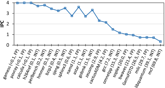
We observe from Figure 27 that, in general, the overall IPC of desktop and scientific applications decreases as the MPKI increases. However, there are two notable exceptions: namd and gobmk. We discuss how these exceptions are the result of differences in bank parallelism utilization (BPU) in Section 5.1. Figure 28 shows the BPU of each application when run with the DDR3 DRAM type. Note that our DDR3 configuration, with four channels, and eight banks per channel, has a total of 32 banks available. Thus, the theoretical maximum BPU is 32, though this does not account for (1) request serialization for banks that share a memory channel or that are part of the same bank group, or (2) maintenance operations such as refresh that reduce the bank parallelism of requests. As we observe from the figure, none of our desktop and scientific applications come close to the maximum BPU. We find that namd and gobmk exhibit much higher BPU values than other applications with similar MPKI values. This indicates that these two applications often issue their memory requests in clusters, i.e., they have bursty memory access patterns. As a result, these two applications exploit memory-level parallelism (MLP), where the latencies of multiple memory requests are overlapped with each other, better than other applications. This increased MLP reduces the application stall time (ghose.isca13, ; qureshi.isca06, ; mutlu.hpca03, ; mutlu.micro07, ; mutlu.ieeemicro06, ; kirman.hpca05, ; das.micro09, ), which in turn increases the IPC of the application.
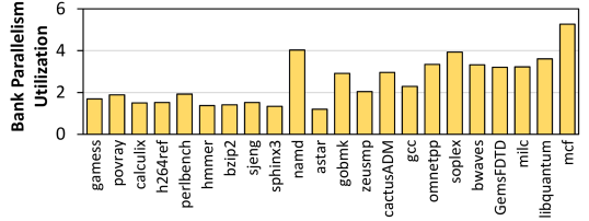
Figure 29 shows the row buffer locality of each single-threaded desktop/scientific application when run on DDR3. We do not see a correlation between the memory intensity of an application and its row buffer locality. This suggests that the locality is predominantly a function of the application’s memory access patterns and row buffer size, and is not related to memory intensity (as expected). We compare the row buffer locality under DDR3 to the row buffer locality with our other DRAM types (not shown for brevity). We find that, with the exception of HMC (which reduces the row width by 97%), row buffer locality characteristics remain similar across different DRAM types.
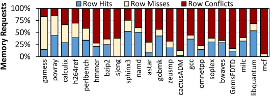
D.2. Multithreaded Desktop/Scientific Applications
To gain insight on limiting factors on the scalability of our multithreaded applications (see Section 6), we study the MPKI and IPC of each application when run using DDR3-2133, and when the application runs with 1, 2, 4, 8, 16, and 32 threads. Figure 30 shows the per-thread IPC for all 12 applications, when the applications are run with one thread and with 32 threads, and lists both the 1-thread and 32-thread MPKI (which quantifies the memory intensity of the application). We observe from the figure that unlike our single-threaded desktop/scientific applications, many of our multithreaded applications maintain a relatively high IPC even at 32 threads, despite the high memory intensity. This is often because multithreaded applications are designed to strike a careful balance between computation and memory usage, which is necessary to scale the algorithms to large numbers of threads. As a result, several memory-intensive multithreaded applications have significantly higher IPCs when compared to single-threaded desktop/scientific applications with similar MPKI values. We note that as a general trend, multithreaded applications with a higher MPKI tend to have a lower IPC relative to multithreaded applications with a lower MPKI.
As an example, we see that miniFE becomes more memory-intensive as the number of threads increases, with its MPKI increasing from 11.5 with only one thread to 68.1 with 32 threads. Despite this increase in memory intensity, its per-thread IPC remains around 1.5, indicating that the application is not completely memory-bound. Prior work (balaprakash.ispass13, ) corroborates this behavior, with an analysis of miniFE showing that in its two hotspot functions, the application spends about 40% of its time on load instructions, but also spends about 40% of its time on integer or floating-point instructions. This exemplifies the balanced approach between computation and memory that most of our multithreaded applications take, regardless of their memory intensity.
D.3. Server and Cloud Workloads
To characterize our server and cloud workloads (see Section 7), we study their performance and memory intensity using the DDR3 DRAM type. Figure 31 shows the performance of each application (IPC; see Section 4), and lists its MPKI. As we see from the figure, the IPC of all of the applications is very high, with the lowest-performing application (Apache2) having an IPC of 1.9 (out of a maximum possible IPC of 4.0). The high performance is a result of the low memory utilization of our server and cloud workloads, which are highly optimized to take advantage of on-chip caches.
Appendix E DRAM Power Breakdown
Figure 32 shows the breakdown of power consumed by the five DRAM types for which we have accurate power models, averaged across all of our single-threaded applications and across our multiprogrammed workloads from Section 5. We observe that all of the evaluated DRAM types consume a large amount of standby power (we simulate a DRAM capacity of ), with DDR3’s standby power representing 77.8% of its total power consumption. As the density and capacity of DRAM continues to increase, the standby power consumption is expected to grow as well. However, the total power consumed varies widely between DRAM types. For example, for our single-threaded desktop and scientific workloads, GDDR5 consumes 2.25x the power of DDR3, while LPDDR4 consumes 67.7% less power than DDR3.
Across all of our workloads (including other workload categories, not shown for brevity), we observe three major trends: (1) standby power is the single biggest source of average power consumption in standard-power DRAM types (because most of the DRAM capacity is idle at any given time); (2) LPDDR3 and LPDDR4 cut down standby power consumption significantly, due to a number of design optimizations that specifically target standby power (see Appendix A); and (3) workloads with a high rate of row conflicts and/or row misses spend more power on activate and precharge commands, as a new row must be opened for each conflict or miss.