Structural origins of electronic conduction in amorphous copper-doped alumina
Abstract
We perform an ab initio modeling of amorphous copper-doped alumina (a-Al2O3:Cu), a prospective memory material based on resistance switching, and study the structural origin of electronic conduction in this material. We generate molecular dynamics based models of a-Al2O3:Cu at various Cu-concentrations and study the structural, electronic and vibrational properties as a function of Cu-concentration. Cu atoms show a strong tendency to cluster in the alumina host, and metallize the system by filling the band gap uniformly for higher Cu-concentrations. We also study thermal fluctuations of the HOMO-LUMO energy splitting and observe the time evolution of the size of the band gap, which can be expected to have an important impact on the conductivity. We perform a numerical computation of conduction pathways, and show its explicit dependence on Cu connectivity in the host. We present an analysis of ion dynamics and structural aspects of localization of classical normal modes in our models.
I Introduction
Non-volatile memory devices based on resistive switching characteristics have been studied since the late 1960s Simmons and Verderber (1967). In these devices, application of an external bias potential across an electrolyte changes the electrical conductivity of the electrolyte by changing its structure. This process is reversible and can be performed in the time scale of nanoseconds. Three types of resistive random access memory (RRAM) devices have been studied in detail Waser et al. (2009) and these include RRAM based on oxygen vacancies, RRAM based on thermo-chemical effects and RRAM based on the electro-chemical metallization. The later class of devices are also called conducting bridge random access memory or CBRAM. The CBRAM devices are composed of a thin solid electrolyte layer placed between an oxidizable anode ( Cu, Ag or TiN) and an inert cathode ( W or Pt). The Cu, in its ionic state, is converted into the conducting “filament” by the applied field: the ions are reduced by electrons flowing from the cathode to leave them in their metallic form, although other counter ions (e.g., OH-) may also be involved in this process Tappertzhofen et al. (2013). With the application of a reverse bias, the connectivity of the cluster can be destroyed, and the device is put into a highly electronically resistive state. The details of the mechanism of CBRAMs have been described elsewhere Kozicki and Barnaby (2016); Dietrich et al. (2007). The performance of CBRAM devices has been studied with several materials as the solid electrolyte which include chalcogenides Kund et al. (2005); Lee et al. (2017), insulating metal oxides Chen et al. (2017); Tsuruoka et al. (2010); Gu et al. (2010); Xu et al. (2014); Belmonte et al. (2013, 2015); Pandey et al. (2015) and bilayer materials Tsai et al. (2016); Barci et al. (2016). CBRAM devices have demonstrated excellent performance in terms of operational voltage, read/write speed, endurance and data retention. Among the host materials reviewed for CBRAM devices, alumina (Al2O3) shows particular promise. It has a high dielectric constant, large band gap, and its amorphous phase is highly stable Kittl et al. (2009); Eklund et al. (2009). The experimental results for CBRAM devices based on Cu alloyed with Al2O3 have shown that the cell exhibits highly controlled set and reset operations, fast pulse programming (10 ns) at low voltage (<3 V) and low-current (10 A) with 106 cycles per second for the writing speed Belmonte et al. (2013).
In this paper, we use ab initio molecular dynamics (AIMD) to generate atomic models of a-Al2O3:Cu and investigate the microscopic origin of elctronic conduction in this material. The work presented in this paper shows that an increase in local Cu-concentration can result in stable conducting pathways due to the strong tendency of Cu atoms to cluster in the ionic host. This would lead to a highly stable low resistance state (LRS) for high copper concentration, which does indeed seem to be the case for copper-alumina devices Belmonte et al. (2013). We study the electronic properties for these models and are able to crudely estimate the local concentration of Cu above which CBRAM device switch to the LRS. We present the numerical computation of conduction-active parts of the network based on our recent work on computing space projected conductivity (SPC) Prasai et al. (2018), and show that the strong electron-lattice coupling for electron states near the gap leads to interesting and substantial thermally induced conductivity fluctuations on a picosecond time scale.
The rest of the paper is organized as follows. Section II describes computational details used to create the structures and also the details of our method to obtain the SPC. Section III includes results where we discuss structural, electronic and vibrational properties of the models in different subsections. Section IV provides the conclusions.
II Computations
II.1 Model Generation
In this work, we use AIMD to generate four atomic models with the composition of (a-Al2O3)1-nCun with 0, 0.1, 0.2 and 0.3. We used a density of 3.175 g/cm3 for a-Al2O3 Gutiérrez et al. (2000); Vashishta et al. (2008). For the Cu-doped models, we referred to the literature Miranda Hernández J.G. and Rocha-Rangel (2006) to make an initial guess, then carried out a zero-pressure relaxation to correct/optimize the result. For each model, we began by taking a cubic supercell of 200 atoms with randomly initialized positions of the atoms. Plane wave density functional calculations were performed using the VASP package Kresse and Hafner (1993) and projector-augmented wave (PAW) Blöchl (1994); Kresse and Joubert (1999) potentials within the local density approximation (LDA) Perdew and Zunger (1981) using periodic boundary conditions. We used a kinetic energy cutoff of 420 eV and the -point to sample the Brillouin zone. A time step of 1.5 fs was used and the temperature was controlled by a Nosé-Hoover thermostat throughout.
We performed a melt-quench simulation Drabold (2009) with a starting temperature of 3500 K. After annealing the “hot liquid” for 7.5 ps at 3500 K, we cooled each model to 2600 K at a rate of 0.27 K/fs as discussed in reference Momida et al. (2006a) and then equilibrated for 10 ps. Each model was then quenched to 300 K at the same cooling rate 0.27 K/fs and further equilibrated for another 10 ps. Zero pressure relaxations were used to determine the final densities for Cu-doped models. The final force between the atoms is no more than 0.01 eV/atom. The initial and final densities are provided in table 1.
| Cu content | Mol. Formula | (g/cc) | (g/cc) |
|---|---|---|---|
| 0% | (Al2O3)1.00Cu0.00 | 3.175 | 3.175 |
| 10% | (Al2O3)0.90Cu0.10 | 3.58 | 3.75 |
| 20% | (Al2O3)0.80Cu0.20 | 3.78 | 3.99 |
| 30% | (Al2O3)0.70Cu0.30 | 4.53 | 4.82 |
II.2 Spatial Projection of Electronic Conductivity
In this section, we discuss a method to obtain a space projected electronic conductivity. We discuss the method in detail in Ref. Prasai et al. (2018). We begin by writing the diagonal elements of the conductivity tensor for each k-point k and frequency using the standard Kubo-Greenwood formula KGF Kubo (1957); Greenwood (1958) as:
| (1) | |||
In the above equation (1), e and m represent the charge and mass of the electron respectively. represents the volume of the supercell. We average over diagonal elements of conductivity tensor(). is the Kohn-Sham orbital associated with energy and denotes the Fermi-Dirac weight. is the momentum operator along each Cartesian direction . Let
Then suppressing the explicit dependence of on k and , the conductivity can be expressed as:
| (2) |
a form that reminds of the the current-current correlation function origins of Kubo’s approach. If we define complex valued functions on a real space grid (call them x) with uniform spacing of width h in three dimensions, then we can approximate the integrals as a sum on the grid. Thus, Eq. (2) can be written as:
| (3) |
In the preceding, the approximation becomes exact as . If we define a Hermitian, positive-semidefinite matrix:
| (4) |
we can spatially decompose the conductivity at each grid point as . contains vital information about the conduction-active parts of the system111A simpler scheme is to just look at the structure of the Kohn-Sham eigenfunctions near the Fermi level to identify the conduction active parts of the network. While this is a sensible first approximation, it entirely neglects the current-current correlations that underlie the derivation of The Kubo formula from linear response theory..
To implement the method, we used VASP and associated Kohn-Sham orbitals . We divided the supercell into grid points and obtained the wavefunction at each point by using the convenient code of R. M. Feenstra and M. Widom Feenstra and Widom (2012). In computing the , we used a centered finite-difference method to compute the gradient of for each . We used an electronic temperature of T = 1000 K for the Fermi-Dirac distribution. We approximated the function in Eq. (1) by Gaussian distribution of width kT, where k is Boltzmann’s constant.
III Results
III.1 Bonding and topology of the models
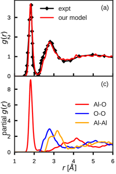
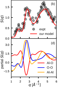
As a test of validity of our models, we compute the total radial distribution function, , on a-Al2O3 models and compare with experimentally measured neutron scattering from Lamparter and Kniep (1997). A plot showing these two is presented in Fig. 1 and shows that the models capture the structural order upto 6 Å reasonably well. We also compute the structure factor, , on our models at 2600 K and compare it with measured on l-Al2O3 Landron et al. (2001). The plot shows that these two show a satisfactory agreement, especially on the positions of peaks at 1.8 Å-1, 2.8 Å-1, 4.7 Å-1. The bottom left plot in Fig. 1 presents the partial computed on models of a-Al2O3. The peaks at 1.81 Å, 2.78 Å and 3.17 Å correspond to the geometrical bond distances for Al-O, O-O and Al-Al pairs respectively; these results are in agreement with similar earlier works Chagarov and Kummel (2009); Momida et al. (2006b); Sankaran et al. (2012). The bottom right plot in Fig. 1 shows the partial corresponding to Al-Al, Al-O and O-O pairs computed on a-Al2O3 models. We see that the first peak in the total occurs at 2.8 Å-1 due to the partial cancellation arising from Al-O correlations.
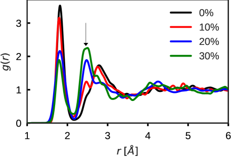
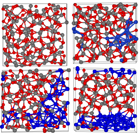
For doped models, the computed are plotted in Fig. 2 and shows that the position of first peak remains largely the same as undoped a-Al2O3 suggesting that Al-O bond remains unaltered. As the concentration of Cu increases, a hump corresponding to Cu-Cu correlation appears and grows at 2.44 Å. The relative sharpness of Cu-Cu hump, even for the lowest concentration of Cu, provides a hint that Cu atoms are probably clustered. Indeed, a visual inspection of the models, shown here in Fig. 3, clearly shows the strong tendency of Cu-atoms to cluster.
It is significant that Cu strongly tends to cluster. A study by Dawson and Robertson Dawson and Robertson (2016) asserts that the Cu-Cu interactions become more favorable with increasing Cu content. We study the average coordination number around Cu atom at different Cu-concentrations as shown in table 2. We take the first minima in partial as the cutoff distance to define the coordination number. The increase in Cu-coordination by Cu and the decrease in Cu-coordination by Al and O supports the segregation of Cu from the host and formation of cluster.
| Cu content(%) | Cu-O | Cu-Cu | Cu-Al |
|---|---|---|---|
| 10 | 1.15 | 5.1 | 3.0 |
| 20 | 0.68 | 6.85 | 2.45 |
| 30 | 0.48 | 8.27 | 1.78 |
III.2 Electronic structure
III.2.1 Density of States and the Localization
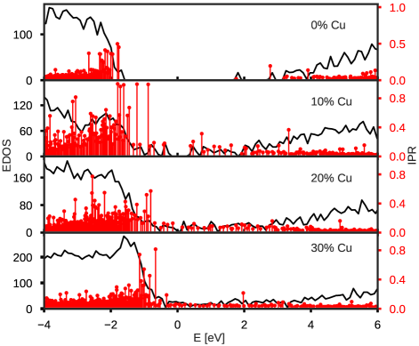
Doping by copper in a-Al2O3 is expected to have effects on electronic properties which are of interest for applications of these materials in CBRAM devices. We investigate these effects by examining the density of Kohn-Sham eigenstates (EDOS) and their spatial localization. The localization is gauged by computing the inverse participation ratio (IPR) that is defined as IPR= Ziman (1979), where the ’s are the contribution to eigenfunction from the atomic projected orbital obtained from VASP. Fig. 4 shows the computed EDOS and IPR as a function of Cu-concentration. We find a decrease in HOMO-LUMO gap with increasing Cu-concentration; at Cu-concentration 20% and 30%, The EDOS is continuous across the Fermi level. The states that fill-in the band gap are quite extended as indicated by small values of IPR around the Fermi level in Fig. 4.
The mean IPR values around the gap declines monotonically with Cu-concentration.
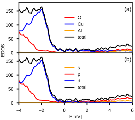
By projecting the electronic states onto atomic sites, we observe that the states near the Fermi level for the doped models consist of Cu-orbitals. An example of the site projected EDOS, for 20% Cu, is plotted in Fig. 5. It is quite interesting that at 20% and 30% Cu-concentrations, Cu levels almost uniformly fill the host a-Al2O3 gap. The Cu does not form an impurity band, as one might naively suppose from experience on heavily-doped semiconductors. We see that models with higher Cu-concentration produce states near Fermi level that yield an essentially metallic form of conduction. This is qualitatively different than the case of Ag in GeSe3 Prasai et al. (2017), wherein the Ag atoms do not cluster and do not introduce states in the optical gap of the host. We observe that electron states in the gap are filled mostly by 3d, 4s and 4p orbitals of Cu.
III.2.2 Charge analysis on Cu atoms
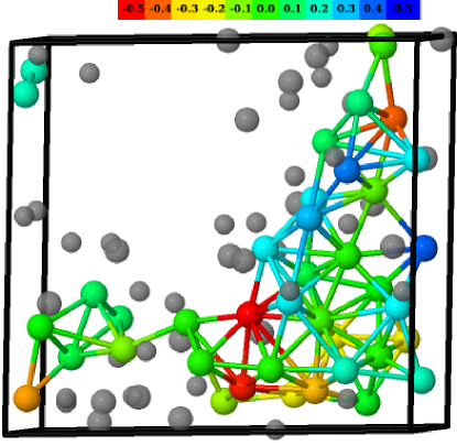
The formation of Cu-cluster in a-Al2O3 matrix leaves the Cu atoms in different charge states depending on the local environment of these Cu atoms with O and/or Al atoms. We performed Bader charge analysis Tang et al. (2009) to calculate net charge on these atoms and an analysis for 20% Cu-doped model is shown in Fig. 6. The charge state of the Cu atoms (shown in color in Fig. 6) can be explained by a simple analysis of the first neighbors around the Cu atoms. Among all the Cu-atoms shown in the figure, only five Cu atoms have exclusively Cu neighbors and are neutral in nature; the rest of the Cu are neighbors with at least one Al or O atoms. When a Cu atom is a neighbor with Al or O atoms, bonding or charge transfer occurs. A Cu atom bonded with O atoms is positively charged, whereas a Cu atom bonded with Al atoms is slightly negatively charged and can be understood in terms of difference in electronegativities of Cu and Al. When a Cu atom is bonded with both O and Al atoms, it is charge neutral. The charge compensation likely to happen in such bonding. The Cu atoms shown in green are therefore almost metallic in nature and are likely to form a conducting channel for the current to flow in the network.
III.2.3 Thermally driven conduction fluctuations
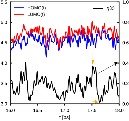
In this section, we discuss relatively dramatic thermally-induced fluctuations in the HOMO-LUMO splitting and consider the electronic conduction mechanisms222Here and elsewhere in this paper, electronic time evolution refers only to variation in Kohn-Sham eigenvalues/states on the Born-Oppenheimer surface – no attempt is made to solve a time-dependent Kohn-Sham equation. We illustrate with one of the conducting models (including 20% Cu) and performed molecular dynamics (MD) at 1000 K for 24 ps. The fluctuation of the frontier HOMO and LUMO levels with time is provided in Fig. 7. is the HOMO-LUMO splitting through the course of the MD. The model reveals a large thermally driven fluctuation in the value of the HOMO-LUMO gap with time.
To physically interpret the connection of the gap with electronic conductivity (), let us write a simple expression for the dc conductivity (T = 0 K) following Mott and Davis Mott and Davis (1979),
| (5) |
where is a matrix element of between Kohn-Sham states near the Fermi level and () is the density of states. So, for dc conduction to occur, there needs to be finite density of states at the Fermi level (to enable electronic transitions, as from Fermi’s Golden Rule) and non-vanishing matrix elements as in Eq. (1). We expect more available states near the Fermi level for the system with small gap, thus the conductivity can be very crudely linked to (small large ) in the spirit of Landau-Zener tunneling Landau (1932); Zener (1932). We provisionally interpret the small gap (small ) instantaneous configurations as low resistance states, and the large gap configurations as high resistance states.
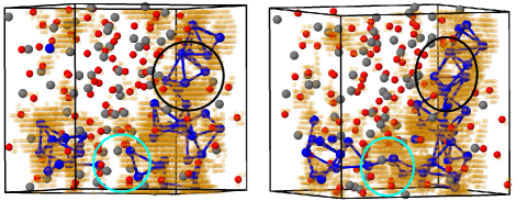
It is therefore interesting to visualize the conduction-active parts of the network for these different states. We selected two snapshots (shown by orange arrows in Fig. 7), one representing a small gap (low ) and the other large gap (high ) from the simulation and obtained the SPC as described in section II.2. The variation of the HOMO-LUMO gap due to thermal fluctuations has also been studied in Boron-doped -Si at 600 K, where it was observed that with addition of hydrogen to the network, there occurs a thermal modulation of HOMO and LUMO states causing the HOMO and LUMO states to be overlapped at a certain interval of the thermal simulation representing highly conducting configuration Pandey et al. (2014). This computation makes it clear that the DC conductivity is difficult to accurately estimate, since to handle the large electron-phonon coupling for states near the Fermi level, long MD averages at constant temperature would be required (within an adiabatic picture for which one simply averages the Kubo formula over a trajectory.
III.2.4 Space-Projected Conductivity
We investigated SPC by computing as described in section II.2 in our models. SPC values are evaluated at coarse 3D grid points inside the supercells. A graphical representation of SPC values in 3D grid points overlaid with the atomic configuration is shown in Fig. 8. This figure shows the SPC computed on two models: one with large and the other with and small . We include 12% of the highest local contributions to SPC in each plot. The SPC reveals that the conduction path is primarily along interconnected Cu atoms. A few O atoms in the vicinity of Cu atoms also participate in the conduction whereas Al atoms do not show any role in the conduction. We see that the SPC for the large gap snapshot is disconnected so that appears to be localized in certain region whereas the SPC with small gap forms an interconnected chain for the conduction. For these two particular structures, we observed the local configurations as shown by the enclosed circles of Fig. 8 where the Cu atoms come closer to form short bonds and form a closed network. This shows that the connectivity among Cu atoms determines the conductivity of the system. Besides the structural difference, the type and the number of clusters also affect the HOMO-LUMO gap. It has been shown that an alternation of the HOMO-LUMO gap occurs between even and odd numbered isolated clusters due to electron-pairing effects and particularly large gap for cluster size 2, 8, 18, 20, 34 and 40 which are also called as magic clusters Kabir et al. (2004). At this temperature, the diffusion of Cu atoms may cause the change in the bonding environment of Cu atoms resulting in the variation of the gap with time.
III.3 Ionic motion
As a representative example, the 20% model was annealed at different temperatures 800 K and 1000 K for 15 ps, and the resulting ion dynamics were studied by calculating the mean-squared displacement for each atomic species as:
| (6) |
where represents the number of atoms of species , represents the position of atom at time t, and the represents an average on the time steps and/or the particles. The connection between mean-squared displacement and the self-diffusion coefficient is given by Einstein’s relation
| (7) |
where is the self-diffusion coefficient, is a constant and is the simulation time.
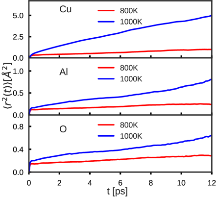
Figure 9 shows the mean-squared displacement for the corresponding species. Clearly, Cu atoms are more diffusive than Al and O atoms. On taking the snapshots of the position of atoms (figures not shown here), we find that the Cu atoms do not diffuse into the host matrix but diffuse within the Cu clusters and thus the Cu clusters become stable at these range of temperatures. We then calculated the self-diffusion coefficient for each species using Eq. (7). The diffusion coefficient for Cu at 800 K and 1000 K are obtained to be and respectively. Cu is relatively static in a-Al2O3 compared to chalcogenides Prasai and Drabold (2011).
III.4 Lattice Dynamics
We study the lattice dynamics of these Cu-doped systems by the means of vibrational density of states (VDOS), species projected VDOS and the vibrational IPR. The properties are studied within the harmonic approximation using the first principles method. The dynamical matrix is obtained by displacing each atoms by 0.015 Å along , and directions. The diagonalization of the dynamical matrix yields eigenfrequencies and the corresponding eigenmodes. The normalized VDOS and the partial VDOS are expressed as Pasquarello et al. (1998)
| (8) | ||||
| (9) |
where are the normalized eigenfrequencies (3N in total). Here, the sum over is over all the atoms belonging to the species and corresponds to the displacement vector of atom with Cartesian components where = x, y and z. We approximate the function by a Gaussian distribution function of width 10 . Among the 3N eigenmodes, we neglect the first three translational modes with frequency very close to zero.
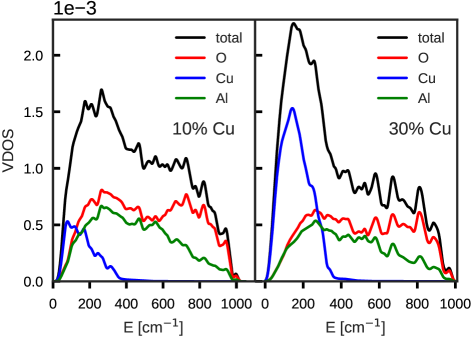
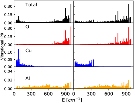
Figure 10 shows the total and partial VDOS for 10% and 30% Cu content. The lower vibrational modes correspond to the Cu atoms. The higher frequency modes are unsurprisingly dominated by O atoms. To study the localization of the vibrational eigenstates, we calculated the vibrational IPR for each species. From Fig. 11, we see that the higher modes corresponding to the O atoms are more localized compared to the lower modes for both concentrations of Cu. The lower eigenstates corresponding to Cu for 10% Cu model are quite localized compared to the 30% Cu model. The vibrational states for aluminum are mostly extended for both models.
IV Conclusion
In this paper, we studied realistic models of a-Al2O3:Cu, and showed that the Cu atoms have a strong propensity to cluster in the ionic a-Al2O3 host. We observed a continuous filling of the optical gap by Cu levels, especially at 20% and 30% models. As the Cu-concentration increases (and Cu-Cu connectivity increases), the Cu levels band to enable metallic conduction. We observed the opening and closing of the HOMO-LUMO gap at an elevated temperature, and projected electronic conductivity into real space and visualized the conduction-active parts of the network. We showed that the connectivity of Cu atoms play a significant role in the electronic conduction. We studied the diffusion of Cu atoms in a-Al2O3 at different temperatures and observed that the Cu atoms do not diffuse easily into the a-Al2O3 in contrast with relatively covalent chalcogenides like GeSe3 Prasai and Drabold (2011). We discussed the harmonic lattice dynamics of the models by calculating vibrational density of states and the vibrational IPR and showed that the lower vibrational modes correspond to Cu atoms and the higher modes correspond to O atoms.
The results presented in this work on a-Al2O3:Cu show an interesting contrast with similar study performed on GeSe3:Ag Subedi et al. (2019). We find that the properties of Cu in the oxide host (in this case, a-Al2O3:Cu) contrast with that of Ag in chalcogenide (in case of Subedi et al. (2019), GeSe3:Ag). The Ag atoms do not form a cluster in the GeSe3 and no uniform filling of the optical gap is observed. In other words, one has to electrochemically work hard to draw Ag atoms together to form a cluster in GeSe3. So, the electronic conduction is likely to occur by hopping process in GeSe3:Ag whereas the conduction in Al2O3:Cu is most likely through the interconnected Cu atoms in the network. We observed that Cu in a-Al2O3 exhibits different charge states (negative, neutral and positive) whereas the charge state of Ag in GeSe3 changes from neutral when isolated to ionic (positive) near the trapping center sites (host atoms) Chaudhuri et al. (2009).
V Acknowledgments
We thank US NSF support under grants DMR 1507670 and 1506836. We thank NVIDIA Corporation for donating a Tesla K40 GPU which was used in some of our calculations. Some of this work used the Extreme Science and Engineering Discovery Environment (XSEDE), which is supported by National Science Foundation grant number ACI-1548562, using BRIDGES at the Pittsburgh Supercomputer Center under the allocation TG-DMR180083. We thank Prof. Gang Chen for valuable discussions during this work.
References
- Simmons and Verderber (1967) J. G. Simmons and R. R. Verderber, Radio and Electronic Engineer 34, 81 (1967).
- Waser et al. (2009) R. Waser, R. Dittmann, G. Staikov, and K. Szot, Advanced Materials 21, 2632 (2009).
- Tappertzhofen et al. (2013) S. Tappertzhofen, I. Valov, T. Tsuruoka, T. Hasegawa, R. Waser, and M. Aono, ACS Nano 7, 6396 (2013).
- Kozicki and Barnaby (2016) M. N. Kozicki and H. J. Barnaby, Semiconductor Science and Technology 31, 113001 (2016).
- Dietrich et al. (2007) S. Dietrich, M. Angerbauer, M. Ivanov, D. Gogl, H. Hoenigschmid, M. Kund, C. Liaw, M. Markert, R. Symanczyk, L. Altimime, S. Bournat, and G. Mueller, IEEE Journal of Solid-State Circuits 42, 839 (2007).
- Kund et al. (2005) M. Kund, G. Beitel, C. . Pinnow, T. Rohr, J. Schumann, R. Symanczyk, K. Ufert, and G. Muller, in IEEE InternationalElectron Devices Meeting, 2005. IEDM Technical Digest. (2005) pp. 754–757.
- Lee et al. (2017) D. Lee, S. Oukassi, G. Molas, C. Carabasse, R. Salot, and L. Perniola, IEEE Journal of the Electron Devices Society 5, 283 (2017).
- Chen et al. (2017) W. Chen, S. Tappertzhofen, H. J. Barnaby, and M. N. Kozicki, Journal of Electroceramics 39, 109 (2017).
- Tsuruoka et al. (2010) T. Tsuruoka, K. Terabe, T. Hasegawa, and M. Aono, Nanotechnology 21, 425205 (2010).
- Gu et al. (2010) T. Gu, T. Tada, and S. Watanabe, ACS Nano 4, 6477 (2010).
- Xu et al. (2014) X. Xu, J. Liu, and M. P. Anantram, Journal of Applied Physics 116, 163701 (2014).
- Belmonte et al. (2013) A. Belmonte, W. Kim, B. Chan, N. Heylen, A. Fantini, M. Houssa, M. Jurczak, and L. Goux, in 2013 5th IEEE International Memory Workshop (2013) pp. 26–29.
- Belmonte et al. (2015) A. Belmonte, U. Celano, R. Degraeve, A. Fantini, A. Redolfi, W. Vandervorst, M. Houssa, M. Jurczak, and L. Goux, IEEE Electron Device Letters 36, 775 (2015).
- Pandey et al. (2015) S. C. Pandey, R. Meade, and G. S. Sandhu, Journal of Applied Physics 117, 054504 (2015).
- Tsai et al. (2016) T. Tsai, F. Jiang, C. Ho, C. Lin, and T. Tseng, IEEE Electron Device Letters 37, 1284 (2016).
- Barci et al. (2016) M. Barci, G. Molas, C. Cagli, E. Vianello, M. Bernard, A. Roule, A. Toffoli, J. Cluzel, B. D. Salvo, and L. Perniola, IEEE Journal of the Electron Devices Society 4, 314 (2016).
- Kittl et al. (2009) J. Kittl, K. Opsomer, M. Popovici, N. Menou, B. Kaczer, X. Wang, C. Adelmann, M. Pawlak, K. Tomida, A. Rothschild, and et al., Microelectronic Engineering 86, 1789 (2009).
- Eklund et al. (2009) P. Eklund, M. Sridharan, G. Singh, and J. Bøttiger, Plasma Processes and Polymers 6, S907 (2009).
- Prasai et al. (2018) K. Prasai, K. N. Subedi, K. Ferris, P. Biswas, and D. A. Drabold, physica status solidi (RRL) – Rapid Research Letters 12, 1800238 (2018).
- Gutiérrez et al. (2000) G. Gutiérrez, A. B. Belonoshko, R. Ahuja, and B. Johansson, Physical Review E 61, 2723 (2000).
- Vashishta et al. (2008) P. Vashishta, R. K. Kalia, A. Nakano, and J. P. Rino, Journal of Applied Physics 103, 083504 (2008).
- Miranda Hernández J.G. and Rocha-Rangel (2006) A. Miranda Hernández J.G., Soto Guzmán and E. Rocha-Rangel, J.Ceram. Proc. Res 7, 311 (2006).
- Kresse and Hafner (1993) G. Kresse and J. Hafner, Phys. Rev. B 47, 558 (1993).
- Blöchl (1994) P. E. Blöchl, Phys. Rev. B 50, 17953 (1994).
- Kresse and Joubert (1999) G. Kresse and D. Joubert, Phys. Rev. B 59, 1758 (1999).
- Perdew and Zunger (1981) J. P. Perdew and A. Zunger, Phys. Rev. B 23, 5048 (1981).
- Drabold (2009) D. A. Drabold, Eur. Phys. J. B 68, 1 (2009).
- Momida et al. (2006a) H. Momida, T. Hamada, Y. Takagi, T. Yamamoto, T. Uda, and T. Ohno, Phys. Rev. B 73, 054108 (2006a).
- Kubo (1957) R. Kubo, J. Phys. Soc. Jpn. 12, 570 (1957).
- Greenwood (1958) D. A. Greenwood, Proceedings of the Physical Society 71, 585 (1958).
- Feenstra and Widom (2012) R. M. Feenstra and M. Widom, (2012), www.andrew.cmu.edu/user/feenstra/wavetrans.
- Lamparter and Kniep (1997) P. Lamparter and R. Kniep, Physica B: Condensed Matter 234-236, 405 (1997).
- Landron et al. (2001) C. Landron, L. Hennet, T. E. Jenkins, G. N. Greaves, J. P. Coutures, and A. K. Soper, Phys. Rev. Lett. 86, 4839 (2001).
- Chagarov and Kummel (2009) E. A. Chagarov and A. C. Kummel, The Journal of Chemical Physics 130, 124717 (2009).
- Momida et al. (2006b) H. Momida, T. Hamada, Y. Takagi, T. Yamamoto, T. Uda, and T. Ohno, Phys. Rev. B 73, 054108 (2006b).
- Sankaran et al. (2012) K. Sankaran, L. Goux, S. Clima, M. Mees, J. Kittl, M. Jurczak, L. Altimime, G.-M. Rignanese, and G. Pourtois (Electrochemical Society, 2012) pp. 317–330.
- Dawson and Robertson (2016) J. A. Dawson and J. Robertson, The Journal of Physical Chemistry C 120, 14474 (2016).
- Ziman (1979) J. M. Ziman, Models of disorder : The theoretical physics of homogeneously disordered systems (Cambridge University Press Cambridge [Eng.] ; New York, 1979) pp. xiii, 525 p. :.
- Prasai et al. (2017) K. Prasai, G. Chen, and D. A. Drabold, Phys. Rev. Materials 1, 015603 (2017).
- Tang et al. (2009) W. Tang, E. Sanville, and G. Henkelman, Journal of Physics: Condensed Matter 21, 084204 (2009).
- Mott and Davis (1979) N. F. Mott and E. A. Davis, Electronic processes in non-crystalline materials / by N.F. Mott and E.A. Davis, 2nd ed. (Clarendon Press ; Oxford University Press Oxford : New York, 1979) pp. xiv, 590 p. :.
- Landau (1932) L. D. Landau, Phys. Z. Sowjetunion 2, 46 (1932).
- Zener (1932) C. Zener, Proceedings of the Royal Society of London Series A 137, 696 (1932).
- Pandey et al. (2014) A. Pandey, B. Cai, N. Podraza, and D. A. Drabold, Phys. Rev. Applied 2, 054005 (2014).
- Kabir et al. (2004) M. Kabir, A. Mookerjee, and A. K. Bhattacharya, Phys. Rev. A 69, 043203 (2004).
- Prasai and Drabold (2011) B. Prasai and D. A. Drabold, Phys. Rev. B 83, 094202 (2011).
- Pasquarello et al. (1998) A. Pasquarello, J. Sarnthein, and R. Car, Phys. Rev. B 57, 14133 (1998).
- Subedi et al. (2019) K. N. Subedi, K. Prasai, and D. A. Drabold, arXiv e-prints , arXiv:1901.04324 (2019), arXiv:1901.04324 [cond-mat.dis-nn] .
- Chaudhuri et al. (2009) I. Chaudhuri, F. Inam, and D. A. Drabold, Phys. Rev. B 79, 100201(R) (2009).