Evidence for flat zero-energy bands in bilayer graphene with a periodic defect lattice
Abstract
In this work, we perform ab initio calculations, based on the density functional theory, of the electronic structure of a graphene bilayer with a periodic array of topological defects. The defects are generated by intercalation of carbon atoms between the layers and their subsequent absorption by one of the layers. We use the unit cell of the bilayer to construct larger unit cells (supercells), positioning a single carbon atom in the hollow position between the monolayers and periodically replicating the supercell. By increasing the size of the supercell and, consequently, the periodicity of the inserted atoms, we not only optimize the results but also vary the size of the defect lattice. Our main result is the appearance of a doubly degenerate flat band at the Fermi level. These states are interpreted as coming from the periodic deformation of the bilayer due to the topological defects generated by the inserted atoms. It acts as a non-Abelian flux network creating zero energy flat bands as predicted by San-Jose, González and Guinea in 2012. Since the periodic strain field associated to the defect array has such a strong influence on the electronic properties of the bilayer, it may be useful for practical applications. For instance, it can act as frozen-in magnetic-like field flux tubes. All-carbon nanostructures can then be designed to have electronic behavior at different regions tailored by the chosen defect pattern.
1 Introduction
The advent of carbon-based low-dimensional materials, like nanotubes, fullerenes, single layer graphene (SLG) and bilayer graphene (BLG), to name a few, brought forward very rich physics and a wide range of applications. While SLG has a zero band gap and linear dispersion relation, allowing a description by massless Dirac fermions [1], BLG has an easily tunable electronic band gap and parabolic dispersion relation, when in the A-B, (or Bernal-stacked) form [2]. These differences make BLG more attractive to electronic and photonic applications, without losing its fundamental physics appeal, as illustrated by the recently reported discovery of the exotic 5/2 quantum Hall state in BLG [3] and unconventional supercondutivity in twisted BLG [4]. Moreover, electrons in SLG (BLG) are chiral quasiparticles which, when adiabatically propagated along a closed orbit, acquire a Berry phase of (), according to their degree of chirality [5].
It is well known that mono and bilayer graphene and graphene-based materials have found their way to many technological applications [6]. Nevertheless, other two-dimensional systems like hexagonal boron-nitride (h-BN) [7], phosphorene [8, 9, 10], borophene [11], silicene [12], germanium monosulfide [13, 14], siligraphene [15, 16], etc., also appear as promising materials for nanoelectronics, spintronics and optoelectronics applications.
The recently reported superconductivity in twisted BLG [4, 17] turns it even more important for the study of fundamental physics as well as for applications. Theory has predicted that flat bands, not only enable superconductivity but also can enhance its transition temperature [18]. Flat bands in BLG could be obtained by doping or gating but, in twisted bilayer graphene (TBLG), they arise as a consequence of the moiré pattern associated to the twist [19]. As explained in reference [19], the moiré superlattice appears to the electrons in TBLG as a periodic array of non-Abelian gauge fluxes, which leads to localized Landau-like levels, the flat bands. These flat bands start to form as the pattern period increases. In this work, by doing DFT calculations, we show that BLG periodically intercalated with carbon atoms presents a similar behavior. The inserted atoms bond to one of the layers producing a periodic array of topological defects. We observe localized bands near the defects, which gradually flatten out as the separation between the defects increases. The local deformation of the BLG lattice due to each intercalated atom acts as a pseudomagnetic flux [20, 21, 22] giving rise to the observed localized states. This way, we present evidence that a periodic array of topological defects generated by intercalation of carbon atoms in BLG leads to flat bands as observed in TBLG. An exciting experimental perspective is to combine twisting with the introduction of topological defects, in contrast with twisting plus doping done in [23].
Reference [24] reports an extensive study of periodic arrays of fullerenes incorporated into a single layer graphene sheet, so-called bubble-wrap carbon. The electronic structure there obtained shows clearly the emergence of flat bands. Also, metallic behavior is achieved at high density of the bubbles. Although both SLG and BLG are very important for technological applications, since their basic physics are quite different, it is important to verify if anything similar to what was observed in [24] also happens in BLG. For this end we choose to work with BLG with the simplest “bubble” we could think of, a topological defect formed by the periodic absorption of a carbon atom by one of the layers (see Fig. 2). We focus on the most stable graphene bilayer, which consists of two graphene monolayers stacked in a model known as A-B Bernal phase, in which one of the layers is rotated by relative to one another and the interaction between the layers is of van der Waals type [5]. For recent reviews on electronic properties of this and the other types of BLG see Refs. [25] and [26].
2 Computational Methodology
The graphene bilayer can be obtained experimentally by Chemical Vapor Deposition [27] and its lattice parameters are Å ( and indicate the crystal lattice constants in the plane) [28]. Its unit cell has four atoms and the separation distance between the monolayers is Å [29]. Using these data, we performed first principles calculations of the graphene bilayer intercalated with carbon atoms in the hollow position. The calculations were done using the CASTEP code, which is included in the Materials Studio software package and uses the density functional theory plane-wave pseudopotential method (DFT) [30, 31]. The CASTEP code also uses the generalized gradient approximation (GGA), and the Perdew-Burke-Ernzerhof (PBE) functional [32].
In our calculations we used norm-conserved pseudopotential, which increases the computational cost, but yields good results. The Monkhorst-Pack grid [33] was 11111, for a better analysis of integrals in the reciprocal space. The structures used were optimized with the total minimum energy, in which the maximum energy change during geometry optimization was eV/cell, the maximum force is eV/Å, pressure smaller than GPa, and maximum atomic displacement not exceeding Å. Furthermore, we had a self-consistent field (SCF) tolerance of 1 eV/cell, and convergence window of three cycles. The energy cutoff is eV.
3 Results and discussion
3.1 Geometry optimization
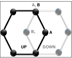
The top view of the Bernal stacking of our system is shown in Fig. 1 where gray represents the lower layer and black represents the upper layer. As we can see, position of the top layer lies exactly above the center of the hexagon of the bottom layer. The position of the upper layer coincides with the position of the lower layer and the position of the lower layer exactly matches the center of the hexagon of the upper layer. Finally, in the hollow position, the atom is above the center of the hexagon formed by the lower monolayer, as shown in Figure 1.


In our study, we used the supercell scheme, in which the cells are periodically arranged in space. We used 4 different sizes for the supercell: 22, 33, 44 and 55, each with 16, 36, 64 and 100 carbon atoms, respectively (not counting the extra atom). The four structures are represented by their supercells in Fig. 2. The lattice parameters of each structure is shown in Table 1. With respect to the lattice parameter , associated to the periodicity in the direction normal to the bilayers, we always used Å to ensure that there is no interaction between the multiple bilayers that arise due to the periodicity of the system.
In the optimization geometry, our structures were relaxed until they reached the convergence criteria. As can be seen in all cases depicted in Fig. 2, the inserted atom binds to the upper layer pushing one of its atoms to an out-of-plane position. Thus, when the C atom joins the monolayer, it does not only assume the position of one of the atoms, but rather reorganizes the bonds in that region, deforming the structure. In fact, as it is clear form Fig. 2, the three neighboring atoms of the one above the intercalated atom change their hybridization from to . Consequently, the intercalated atom and its upstairs neighbor are pushed out of the graphene plane. The resulting structure cannot be relaxed back to the hexagonal lattice without cutting and rejoining chemical bonds, what characterizes a topological defect. The repetition of the supercell with the extra atom in 2D space then generates an infinite BLG with a periodic deformation reminiscent of bubble-wrap graphene [24]. In Fig. 3 it is shown a representation of the lattice generated by the 22 supercell before optimization.
In Table 1 we have the superlattice parameter , which corresponds to the periodicity of the defect array, for each of the structures studied. was obtained from the value for the pristine BLG unit cell, Å, by appropriate scaling. The parameter Å is the same for all structures. is the binding energy of the system, which is obtained from the expression,
| (1) |
where is the energy of the pure bilayer, the energy of a single C atom, and is the energy of the system with the atom intercalated in the bilayer. corresponds to the distance between the intercalated C atom and its closest neighbor in the monolayer. is the distance between the monolayers after the atom is added to the system, whose value for pure bilayers is Å [29].
We observe that the formation energy of BLG(33), BLG(44) and BLG(55) scale approximately with the cell size. The higher value for BLG(22) seems to be due to the interaction between defects in neighboring cells. This effect naturally dies off quickly for larger cells. In all systems investigated, the bond distances between the intercalated atom and the monolayer atom attached to it are very close to the usual single bond distance of Å [34]. The separation of the layers near the defects follows an increasing order as the defect lattice parameter increase, from the lower value Å for the BLG(22) system, to the higher value Å for BLG(55). Away from the defects the separation is Å, which is the value for the pure bilayer. Throughout the text we distinguish the pristine and hollow-intercalated structures by referring, respectively, to BLGp and BLGh.
| BLG(22) | BLG(33) | BLG(44) | BLG(55) | |
|---|---|---|---|---|
| (Å) | 4.92 | 7.38 | 9.84 | 12.30 |
| (eV) | 1.41 | 0.54 | 0.65 | 1.04 |
| aC-layer (Å) | 1.54 | 1.59 | 1.58 | 1.58 |
| (Å) | 3.38 | 3.54 | 3.59 | 3.76 |
For the sake of verification of mechanical and thermodynamical stability of the structures, we also calculated the phonon spectrum, phonon density of states and the thermodynamic functions (enthalpy, entropy, Gibbs free energy, heat capacity and Debye temperature), which will be the subject of a separate publication. We observed that all structures studied are stable, since they present only positive frequencies and can be built spontaneously (an exothermic process).
3.2 Flat zero-energy bands
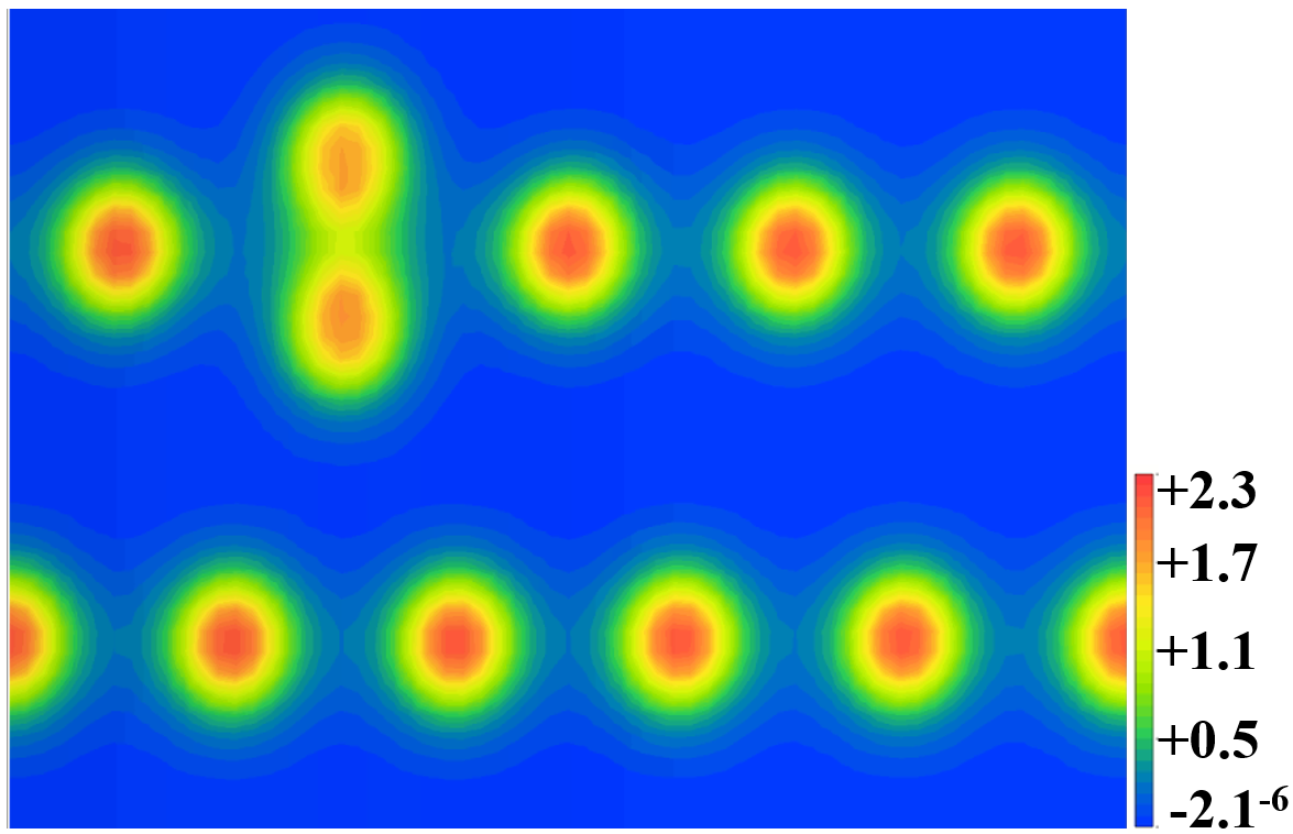
The fact that the intercalated atoms get incorporated into one of the graphene layers without really doping it (not transferring charge) generates a structurally stable lattice of local deformations. For a single graphene layer these deformations are well described [20] by an Abelian gauge field; i.e., a pseudomagnetic field. This gives rise to localized, Landau-like, levels [21]. In the case of the bilayer, the interlayer hopping is affected by the distortions in such a way that the effective field is now non-Abelian [19]. In this reference, it is shown that a periodic pattern, with large periodicity, of such non-Abelian fluxes induces spatial confinement of electronic states in flat bands. As the periodicity of the pattern increases they observed that “the system develops two increasingly narrow sub-bands around zero energy states”. This is exactly what we obtain in our study of periodically C-intercalated BLG, as shown in Fig. 5. Even though the results of Ref. [19] were obtained for sheared or twisted bilayers, in the resulting structure, the interlayer separation is periodically corrugated as it also happens in our system. This is clear in Fig. 4 where we show the charge density profile in a transverse cut of our system.
3.3 Band Structure and Density of States
We now present the calculated energy bands as a function of the periodicity of the defect lattice (or supercell size). The analysis is performed by observing the bands in relation to the points of high symmetry in the first Brillouin zone. We also compute both the total and the spin-resolved density of states (DOS) for each case.
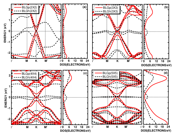
The high symmetry points are in the following sequence: (0.000, 0.000, 0.000), M (0.000, 0.500, 0.000), K (0.333, 0.333, 0.000), M’ (0.500, 0.000, 0.000) and (0.000, 0.000, 0.000). In Fig. 5, we present the calculated band structure and corresponding density of states for each supercell size. For the sake of comparison, each graph includes both BLGh (dotted black lines) and BLGp (red lines).
Ideally, the calculations should be performed for the actual experimental size of the bilayer, which is unfeasible due to the large number of atoms involved. A way of getting by this difficulty is by defining a unit cell and then using periodic boundary conditions. Obviously, one expects that the larger the unit cell the more realistic the results will be. For this matter, we did calculations for four different supercell sizes in order to infer any tendency of convergence of the computed physical observables. Besides improving the quality and reliability of the results, this procedure naturally gives us a way of changing the lattice parameter of the topological defect array. In figure 5 we show the band structure and density of states for the four cases, both with and without the extra carbon atoms. In the pristine bilayer (BLGp) case, the usual gapless parabolic dispersion relation appears clearly for all supercell sizes, in agreement with the literature [35]. For the intercalated BLGh a small band gap appears at the K point which tends to 0.2 eV as one goes to the larger structures. Further, starting at the 33 structure, there appears two energy bands spread around the Fermi level. As the size of the structure increases, those bands converge to a single flat band at the Fermi level. A doubly degenerate zero mode which is clearly seen in the density of states plots of the corresponding structures.
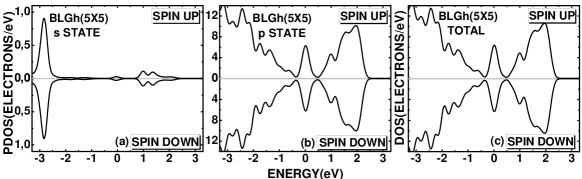
Evidence that the zero modes are localized on the deformed region created by the intercalated atom, comes from Fig. 6. There, we present the spin-resolved projected density of states (PDOS) on the site of the deformation for the 5 structure. The PDOS is shown separately for the and states, as well as for their sum. There is no clear spin separation in the outcome of our calculations which is natural in an all-carbon structure. Furthermore, the fact that both and states have peaks in the same energy region, confirms the hybridization observed in Fig. 2.
The occurrence of the flat bands at zero energy in the larger periodicity BLGh is the main result of this article. We interpret this finding under the light of the pseudomagnetic field associated to distortions of graphene [20, 21, 22]. The extra carbon atoms are incorporated to one of the layers more like a topological defect than as a dopant, since it is an all-carbon structure. Alternatively, the same structures can, in principle, be obtained by suitably cutting bonds, rearranging them, changing the hybridization of the involved atoms from to and reconnecting the appropriate bonds. So, what we have is a periodic array of “bubbles” very much like the bubble-wrap carbon reported in [24]. Incidentally, the band structures shown in reference [24] present almost flat bands near the Fermi level.
4 Conclusion
We performed first-principles calculations for a graphene bilayer periodically intercalated with carbon atoms in the hollow position, using the DFT formalism with the GGA approach and PBE functional, implemented in the CASTEP module. In our study, we worked with four sizes of supercells, therefore increasing the periodicity of the lattice of inserted atoms. The extra atoms are found to bind covalently to one of the layers with hybridization, which introduces an out-of-plane distortion. Since the inserted atoms are of the same species, their inclusion just creates a topological defect, locally deforming the layer. The result is a periodic array of topologically stable deformations in one of the layers. If it were a single layer this would act as an array of pseudomagnetic fluxes threading the structure. Since we have a bilayer, the interlayer hopping is affected by the deformations and we effectively have a non-Abelian gauge field as the one studied in [19]. For each of the systems generated in our study, it was obtained the electronic band structure and density of states. The major difference between the band structure of pristine BLG and the one with the periodic deformation in one of the layers is the appearance of two new bands spread around the Fermi level in the latter. As the period of the deformation lattice increases these two bands get narrower and narrower tending to a single degenerate flat band at the Fermi level. Exactly as predicted in Ref. [19].
It is worth mentioning that flat, or partially flat, bands also appear in bilayer graphene under the application of a perpendicular magnetic field [36]. Moreover, in [36] it is reported that, due to the interaction of the electron spin with the magnetic field, the hybridization is destroyed, leading to a semimetal to metal transition. In a similar way, the destruction of the hybridization is done locally by each topological defect in our system. In this sense, our array of topological defects works very much as a lattice of magnetic flux tubes, locally changing the hybridization. The effect on the electronic structure is the opening of a small gap and the creation of flat bands in the gap. Therefore, a tight-binding calculation along the lines of Ref. [36], for the system studied here, with and without a perpendicular magnetic field, would be very interesting for comparison with our results. Of particular interest, is the comparison between pristine BLG under a perpendicular magnetic field and the bilayer with topological defects, in the limit of a very dense array of defects (without magnetic field). A final comment on this process of destruction of the hybridization, concerning graphene-like structures, is due here. Preliminary results from our group indicate that Bernal h-BN bilayers intercalated with boron atoms also acquire flat bands in the gap, possibly due to a similar mechanism of hybridization change. This is also observed when pristine h-BN bilayer is under the action of a perpendicular magnetic field [36].
Since both pristine SLG and BLG have zero band gaps, engineering both the gap and the band shape is a must for technological applications. Molecular doping [37], use of an applied electric field [38] or even a magnetic field [36] are known means of achieving this. Another possibility, suggested by the results presented here, is a “clean” doping using carbon atoms, or rewiring of the network, in order to create stable topological defects on the all-carbon structure. As seen above, besides opening a gap, this also introduces flat bands in the electronic structure, which opens up new experimental possibilities for gap and band shape control.
Acknowledgments
Financial support from INCT-Nanocarbono, Conselho Nacional de Desenvolvimento Científico e Tecnológico (CNPq), Coordenação de Aperfeiçoamento de Pessoal de Nível Superior (CAPES) and Fundação de Amparo à Ciência e Tecnologia do Estado de Pernambuco (FACEPE) is acknowledged. DLA acknowledges the Mato Grosso Research Foundation - FAPEMAT for financial support through the Grant PRONEX CNPq/FAPEMAT-850109/2009.
5 References
References
- Novoselov et al. [2005] K. S. Novoselov, A. K. Geim, S. Morozov, D. Jiang, M. Katsnelson, I. Grigorieva, S. Dubonos, A. A. Firsov, Two-dimensional gas of massless dirac fermions in graphene, Nature 438 (2005) 197.
- McCann [2006] E. McCann, Asymmetry gap in the electronic band structure of bilayer graphene, Physical Review B 74 (2006) 161403.
- Li et al. [2017] J. Li, C. Tan, S. Chen, Y. Zeng, T. Taniguchi, K. Watanabe, J. Hone, C. Dean, Even-denominator fractional quantum hall states in bilayer graphene, Science 358 (2017) 648–652.
- Cao et al. [2018] Y. Cao, V. Fatemi, S. Fang, K. Watanabe, T. Taniguchi, E. Kaxiras, P. Jarillo-Herrero, Unconventional superconductivity in magic-angle graphene superlattices, Nature 556 (2018) 43.
- McCann and Fal’ko [2006] E. McCann, V. I. Fal’ko, Landau-level degeneracy and quantum hall effect in a graphite bilayer, Physical Review Letters 96 (2006) 086805.
- Coroş et al. [2019] M. Coroş, F. Pogăcean, L. Măgeruşan, C. Socaci, S. Pruneanu, A brief overview on synthesis and applications of graphene and graphene-based nanomaterials, Frontiers of Materials Science 13 (2019) 23–32.
- Brito et al. [2019] E. Brito, L. Leite, S. Azevedo, J. da Rocha Martins, B. de Lima Bernardo, Theoretical investigation of the electronic and optical properties of gallium-doped hexagonal boron nitride through monte carlo and ab initio calculations, Physica E: Low-dimensional Systems and Nanostructures 106 (2019) 277–282.
- Le et al. [2019] P. Le, M. Davoudiniya, K. Mirabbaszadeh, B. Hoi, M. Yarmohammadi, Combined electric and magnetic field-induced anisotropic tunable electronic phase transition in ab-stacked bilayer phosphorene, Physica E: Low-dimensional Systems and Nanostructures 106 (2019) 250–257.
- Le and Yarmohammadi [2019] P. Le, M. Yarmohammadi, Perpendicular electric field effects on the propagation of electromagnetic waves through the monolayer phosphorene, Journal of Magnetism and Magnetic Materials 491 (2019) 165629.
- Le et al. [2019a] P. Le, M. Davoudiniya, M. Yarmohammadi, Perturbation-induced magnetic phase transition in bilayer phosphorene, Journal of Applied Physics 125 (2019a) 213903.
- Le et al. [2019b] P. Le, T. Phong, M. Yarmohammadi, 12-borophene becomes a semiconductor and semimetal via a perpendicular electric field and dilute charged impurity, Physical Chemistry Chemical Physics 21 (2019b) 21790–21797.
- Zhao et al. [2016] J. Zhao, H. Liu, Z. Yu, R. Quhe, S. Zhou, Y. Wang, C. C. Liu, H. Zhong, N. Han, J. Lu, et al., Rise of silicene: A competitive 2d material, Progress in Materials Science 83 (2016) 24–151.
- Zhang et al. [2016] S. Zhang, N. Wang, S. Liu, S. Huang, W. Zhou, B. Cai, M. Xie, Q. Yang, X. Chen, H. Zeng, Two-dimensional ges with tunable electronic properties via external electric field and strain, Nanotechnology 27 (2016) 274001.
- Le et al. [2019a] P. Le, C. V. Nguyen, D. V. Thuan, T. V. Vu, V. Ilyasov, N. Poklonski, H. V. Phuc, I. Ershov, G. Geguzina, N. V. Hieu, et al., Strain-tunable electronic and optical properties of monolayer germanium monosulfide: Ab-initio study, Journal of Electronic Materials 48 (2019a) 2902–2909.
- Le et al. [2019b] P. Le, M. Ebrahimi, M. Davoudiniya, M. Yarmohammadi, Real-space exciton distribution in strained-siligraphene g-sic7, Journal of Applied Physics 126 (2019b) 063104.
- Hussain et al. [2019] T. Hussain, A. H. Farokh Niaei, D. J. Searles, M. Hankel, Three-dimensional silicon carbide from siligraphene as a high capacity lithium ion battery anode material, The Journal of Physical Chemistry C 123 (2019) 27295–27304.
- Cao et al. [2018] Y. Cao, V. Fatemi, A. Demir, S. Fang, S. L. Tomarken, J. Y. Luo, J. D. Sanchez-Yamagishi, K. Watanabe, T. Taniguchi, E. Kaxiras, et al., Correlated insulator behaviour at half-filling in magic-angle graphene superlattices, Nature 556 (2018) 80.
- Kopnin et al. [2011] N. Kopnin, T. Heikkilä, G. Volovik, High-temperature surface superconductivity in topological flat-band systems, Physical Review B 83 (2011) 220503.
- San-Jose et al. [2012] P. San-Jose, J. González, F. Guinea, Non-abelian gauge potentials in graphene bilayers, Physical Review Letters 108 (2012) 216802.
- Manes [2007] J. L. Manes, Symmetry-based approach to electron-phonon interactions in graphene, Physical Review B 76 (2007) 045430.
- Guinea et al. [2010] F. Guinea, M. Katsnelson, A. Geim, Energy gaps and a zero-field quantum hall effect in graphene by strain engineering, Nature Physics 6 (2010) 30.
- Levy et al. [2010] N. Levy, S. Burke, K. Meaker, M. Panlasigui, A. Zettl, F. Guinea, A. C. Neto, M. Crommie, Strain-induced pseudo–magnetic fields greater than 300 tesla in graphene nanobubbles, Science 329 (2010) 544–547.
- Cress et al. [2016] C. D. Cress, S. W. Schmucker, A. L. Friedman, P. Dev, J. C. Culbertson, J. W. Lyding, J. T. Robinson, Nitrogen-doped graphene and twisted bilayer graphene via hyperthermal ion implantation with depth control, ACS nano 10 (2016) 3714–3722.
- Liu et al. [2018] W. Liu, J.-y. Liu, J. Xia, H.-q. Lin, M.-s. Miao, Bubble-wrap carbon: an integration of graphene and fullerenes, Nanoscale 10 (2018) 11328–11334.
- McCann and Koshino [2013] E. McCann, M. Koshino, The electronic properties of bilayer graphene, Reports on Progress in Physics 76 (2013) 056503.
- Rozhkov et al. [2016] A. Rozhkov, A. Sboychakov, A. Rakhmanov, F. Nori, Electronic properties of graphene-based bilayer systems, Physics Reports 648 (2016) 1–104.
- Yan et al. [2011] K. Yan, H. Peng, Y. Zhou, H. Li, Z. Liu, Formation of bilayer bernal graphene: layer-by-layer epitaxy via chemical vapor deposition, Nano letters 11 (2011) 1106–1110.
- Slonczewski and Weiss [1958] J. Slonczewski, P. Weiss, Band structure of graphite, Physical Review 109 (1958) 272.
- Choi and Lee [2016] W. Choi, J.-w. Lee, Graphene: synthesis and applications, CRC press, 2016.
- Hohenberg and Kohn [1964] P. Hohenberg, W. Kohn, Inhomogeneous electron gas, Phys. Rev. 136 (1964) B864.
- Kohn and Sham [1965] W. Kohn, L. J. Sham, Self-consistent equations including exchange and correlation effects, Phys. Rev. 140 (1965) A1133.
- Perdew et al. [1996] J. P. Perdew, K. Burke, M. Ernzerhof, Generalized gradient approximation made simple, Physical Review Letters 77 (1996) 3865.
- Monkhorst and Pack [1976] H. J. Monkhorst, J. D. Pack, Special points for brillouin-zone integrations, Phys. Rev. B 13 (1976) 5188–5192.
- Atkins et al. [2016] P. Atkins, L. Jones, , L. Laverman, Chemical Principles: The Quest for Insight, W. H. Freeman, 2016.
- Ohta et al. [2006] T. Ohta, A. Bostwick, T. Seyller, K. Horn, E. Rotenberg, Controlling the electronic structure of bilayer graphene, Science 313 (2006) 951–954.
- Le et al. [2019] P. T. Le, M. Davoudiniya, M. Yarmohammadi, Interplay of orbital hopping and perpendicular magnetic field in anisotropic phase transitions for bernal bilayer graphene and hexagonal boron-nitride, Physical Chemistry Chemical Physics 21 (2019) 238–245.
- Samuels and Carey [2013] A. J. Samuels, J. D. Carey, Molecular doping and band-gap opening of bilayer graphene, Acs Nano 7 (2013) 2790–2799.
- Kanayama and Nagashio [2015] K. Kanayama, K. Nagashio, Gap state analysis in electric-field-induced band gap for bilayer graphene, Scientific reports 5 (2015) 15789.