An optomechanical platform with a 3-dimensional waveguide cavity
Abstract
At low temperatures, microwave cavities are often preferred for the readout and control of a variety of systems. In this paper, we present design and measurements on an optomechanical device based on a 3-dimensional rectangular waveguide cavity. We show that by suitably modifying the electromagnetic field corresponding to the fundamental mode of the cavity, the equivalent circuit capacitance can be reduced to 29 fF. By coupling a mechanical resonator to the modified electromagnetic mode of the cavity, we achieved a capacitance participation ratio of 43 . We demonstrate an optomechanical cooperativity, 40, characterized by performing measurements in the optomechanically-induced absorption (OMIA) limit. In addition, due to a low-impedance environment between the two-halves of the cavity, our design has the flexibility of incorporating a DC bias across the mechanical resonator, often a desired feature in tunable optomechanical devices.
pacs:
I Introduction
Cavity-optomechanical systems have demonstrated an exquisite ability to control the quantum state of massive-mechanical resonators. A prototypical cavity-optomechanical system consists of an electromagnetic mode and a mechanical mode coupled by radiation-pressure or coulombic-force. braginsky_quantum_1995 ; RevModPhys.86.1391 . Apart from improving the transduction sensitivity metcalfe2014applications , these systems offer a platform to control and manipulate the quantum state of macroscopic mechanical resonators, and to implement tailored interactions brendel_pseudomagnetic_2017 . From earlier demonstrations of achieving quantum ground state, both in optical and in microwave domains teufel_sideband_2011 ; chan_laser_2011 , design and technological advancements in these experimental systems have enabled several milestones such as, capturing a single-microwave photon and its storage in mechanical vibrations reed_faithful_2017 , non-reciprocal microwave circuits peterson_demonstration_2017 ; bernier_nonreciprocal_2017 , hybrid systems with artificial atoms pirkkalainen_hybrid_2013 ; schmidt_ultrawide-range_2018 , and quantum entanglement between two mechanical resonators ockeloen-korppi_stabilized_2018 ; riedinger_remote_2018 .
For optomechanical systems in microwave domain, a common strategy is to couple a mechanically-compliant capacitor to a lumped inductor, or to the distributed inductance of a coplanar waveguide cavity teufel_circuit_2011 ; suh_mechanically_2014 ; andrews_bidirectional_2014 ; teufel_nanomechanical_2009 ; singh2014optomechanical . In this context, 3-dimensional (3D) waveguide cavities provide a unique platform. Due to their intrinsically higher coherence, there has been a lot of interest in using 3D cavities for quantum devices reagor_reaching_2013 . Such cavities have been used for the readout and manipulation of a wide variety of systems such as superconducting qubits paik_observation_2011 , hybrid systems for inter-frequency convertors menke_reconfigurable_2017 , nitrogen-vacancy centers in diamond ball_loop-gap_2018 , and magnons tabuchi_coherent_2015 . To achieve efficient coupling of these systems to electromagnetic field, often one has to engineer the electromagnetic mode to balance the electric and magnetic field components. Primarily due to a large mode volume, 3D cavities have also been used to couple the motion of mm-sized SiN-membrane resonators demonstrating high cooperativity and quantum ground state of motion yuan2015large ; noguchi2016ground . However, in these systems, large parasitic capacitance in the microwave design, and non-lithographic device assembly techniques limit the achieved single photon coupling strength.
In this work, we demonstrate an optomechanical platform based on a 3D-waveguide cavity, where the resonant mode can be engineered to minimize the parasitic capacitance, and thereby achieve a high participation of the mechanically-compliant capacitance. These design guidelines can further be used to develop similar systems with novel materials such as graphene, NbSe2, and to develop hybrid systems with other superconducting circuits while reducing fabrication complexities of the microwave part singh2014optomechanical ; will_high_2017 ; northeast_suspension_2018 . Moreover, our optomechanical system allows to incorporate a DC voltage bias across the mechanically compliant capacitor, thus providing a tunability of mechanical and cavity modes without requiring additional on-chip filter circuitry. The design and low temperature measurements on such a system are described in the following sections.
II Simulations and Design
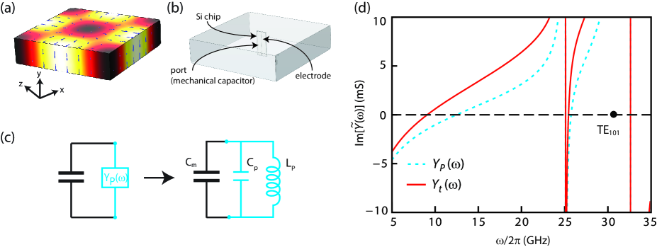
The central idea behind this implementation is to modify the electromagnetic field corresponding to the fundamental TE101 mode of a rectangular waveguide cavity in a manner that maximizes the electric field at its center. A typical distribution of surface charge-current for the fundamental mode is shown in Fig. 1(a). The magnitude of the current drops towards the center of the top and bottom surfaces of the cavity. This is balanced by a corresponding displacement current flowing across the bottom and top surfaces. This suggests that one possible way to maximize the electric field at the center of the cavity could be to direct the charge current towards this region. This is achieved by electrically connecting two electrodes from the middle of the two surfaces (top and bottom), and bringing them closer towards the center, as shown schematically in Fig. 1(b). Thus, an optomechanical system can be formed by placing a mechanically compliant capacitor at the center of the cavity and galvanically connecting its leads to the cavity walls.
Fig. 1(c) shows the equivalent lumped element model, where the “modified-cavity” environment is represented as a complex admittance. The added mechanically compliant capacitor is simulated as a capacitance , which further lowers the resonant frequency of the mode. By applying Foster’s theorem for a loss-less network, the complex-admittance offered by the cavity environment can be decomposed to the equivalent lumped elements foster1924reactance . The mode frequencies ’s of the system are determined by the zeros of the imaginary part of the total admittance, defined by foster1924reactance ; nigg_black-box_2012 . Further, the mode impedance is determined from the positive slope at zero crossing, i.e., . The capacitance and inductance of the corresponding mode are then calculated from and .
We perform numerical simulations to determine the eigen-frequencies with such a major modification to the cavity geometry that extends beyond perturbative analysis nigg_black-box_2012 . With an objective to minimize the parasitic capacitance (cavity-mode capacitance ), we start with a 7 mm 4 mm 7 mm (dimensions along the x, y, z axes as shown in Fig. 1(a)) cavity which has a fundamental resonance mode at 30.3 GHz. We then incorporate a 3 mm 4 mm 0.3 mm (corresponding to the x, y, z axes) silicon chip at the center of the cavity. The chip is designed with a 7 m wide electrode having a 25 m gap at the middle of the cavity. The electrode runs all the way up to the cavity surfaces, forming an electrical short. In the gap between the electrode pattern, we define a lumped port to simulate the admittance seen by the mechanical resonator. The complete geometry is represented in Fig. 1(b) and an image of a real system is shown in Fig. 2(a).
Using finite element methods, we then numerically compute the complex admittance of the environment as seen from this port. In a real device, of course, the port is replaced by a mechanical capacitor and an effective electromagnetic cavity mode is formed by combining a mechanical capacitance to the complex admittance . Since the typical size of the mechanical capacitor is much smaller than the wavelength of the microwave signals, it justifies the choice of a lumped port at the center.
| Cavity size | Electrode width | Mode frequency | |||
|---|---|---|---|---|---|
| (mm3) | (m) | (fF) | (GHz) | (fF) | (nH) |
| 28 6 28 (for device in Fig. 4) | 50 | 7.1 | 6.4 | 148.6 | 4.0 |
| 28 6 28 | 7 | 7.1 | 6.3 | 93.7 | 6.3 |
| 7 4 7 (for device 1 in Fig. 3(c)) | 7 | 23 | 9.4 | 29.8 | 5.4 |
The simulations were performed for various cavity dimensions and device geometries, in order to have a system with a maximum participation ratio. Fig. 1(d) shows plots of the imaginary parts of admittance of the cavity environment , and total admittance in presence of an added mechanical capacitance of 26 fF for the dimensions mentioned earlier. The connecting electrodes have an effect of lowering the bare cavity TE101 mode to 12.5 GHz. The frequency gets reduced further to 9.1 GHz when the mechanical capacitance is added, as indicated by the first zero-crossing with a positive slope in Fig. 1(d). From the slope at the first root of , we estimated a cavity capacitance fF and an inductance nH. For an optomechanical device with fF, it corresponds to a mode impedance of 485 . A summary of simulation results for cavities of different sizes and electrode widths is listed in Table 1. Additional simulation results are included in the supplemental material (SM)SM .
It is interesting to point out here that a large lumped capacitance at the center of the cavity leads to a significant modification of the eigen-modes such that most of the electric field remains concentrated between the lumped capacitor plates. However, the mode still retains some characteristics of a waveguide field distribution, and can be called a lumped-distributive mode, corroborating well with higher harmonics appearing with large spectral range as seen in Fig. 1(d).
III Device fabrication and assembly
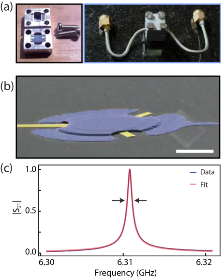
For experimental realization, rectangular waveguide cavities of size 7 mm 4 mm 7 mm were machined using 6061-T5 aluminum alloy, having diamond polished interior surfaces as shown in Fig. 2(a). A more detailed image of the cavity assembly is provided in SM. The bare cavity has a fundamental mode frequency of 30.3 GHz, approximately. In order to lower the electromagnetic mode frequency to within our measurement bandwidth of 4-8 GHz, the mechanical resonator, serving the role of an added capacitor must be designed appropriately. To sufficiently load the electromagnetic mode capacitively, two drumhead-shaped mechanical resonators having their capacitances in parallel were designed. Each resonator has a diameter of 22 m, a gap of 300 nm from the bottom capacitor plate, and is patterned with a 7 m wide connecting electrode. This accounts for approximately 23 fF mechanically compliant capacitance, potentially lowering the cavity mode frequency to 9.4 GHz.
The mechanical resonator device was fabricated on a high resistivity ( 10 k-cm) silicon substrate using multiple steps of optical lithography. The bottom and top electrodes were patterned on 100 nm aluminum films deposited by e-beam evaporation and dc sputtering methods, respectively. The deposition parameters for the top electrode were systematically investigated and optimized to obtain films of high tensile stress. A tilted angle image of one of the mechanical resonators in the drumhead shape is shown in Fig. 2(b). To increase the mechanical capacitance, we pattern two drumhead shaped mechanical resonators having their capacitance in parallel. Such a sample is then placed inside a two port microwave cavity. Patterned electrodes on the chip were wire-bonded to the cavity surface using aluminum wires of 25 m diameter. A complete assembly of the device is shown in Fig. 2(a).
IV Measurements and Analysis
The assembled cavity was mounted to the mixing chamber plate of a dilution refrigerator and cooled down to the base temperature of 20 mK. A sufficiently attenuated input signal was used to drive the cavity and the transmitted signal was first amplified using a low-noise-amplifier and then measured using a vector network analyzer (VNA). In presence of the drumhead-shaped mechanical resonators, the fundamental mode of the cavity was recorded at GHz with a total line width of kHz, as shown in Fig. 2(c). From simulations of the coupling ports, we estimated input and output coupling rates of 96 kHz and 330 kHz, respectively. Since most of the electric field remains in vacuum between the parallel plates of the capacitor, an internal cavity decay rate of 55 kHz is encouraging for future experiments in the quantum regime of motion. As the measured frequency is far off from the simulated value, we suspect the wirebonds ( 2.5 mm long on each side) add a significant inductance to the cavity mode. Kinetic inductance, and reduction in the gap of the mechanical capacitor due to thermal contraction could also be playing a minor role.
The mechanical drumhead resonators and the optomechanical coupling were characterized by performing measurements in the optomechanically induced transparency (OMIT) configuration, wherein two microwave signals are used : a strong pump signal near and a weak probe signal near , where and are the cavity and mechanical resonant frequencies, respectively weis_optomechanically_2010 . In the sideband resolved limit (), the presence of two signals detuned by exerts a beating radiation pressure force on the mechanical resonator, thereby driving it at its resonant frequency. The coherent motion of the mechanical resonator up-converts the sideband signal to exactly the probe frequency . The resulting optomechanical interaction between the microwave field and drum motion manifests in the form of a narrow absorption (OMIA) or a transmission (OMIT) window in an otherwise smooth cavity response.
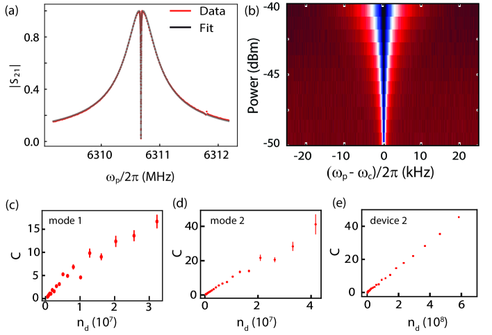
Fig. 3(a) shows the cavity response measured in an OMIT configuration wherein, a sharp dip at the cavity frequency is observed. A small feature near 6.312 GHz corresponds to the second mechanical mode. In presence of a pump tone at the lower sideband (), the cavity transmission is given by,
| (1) |
where and are the coupling efficiencies of the input and output ports, , is the optomechanical cooperativity, is the number of pump photons, and are the cavity and mechanical linewidths, respectively. Measurement results shown in Fig. 3(a) were fitted using Eq. 1. From these measurements, we determine the following parameters for the two mechanical modes: MHz, MHz, intrinsic linewidths of Hz and Hz.
At low pump powers, the linewidth of the OMIA feature is predominantly determined by intrinsic losses in the mechanical resonator, and the magnitude of the cavity transmission at the OMIA feature drops by a factor of . At higher pump powers, the optomechanical damping dominates, leading to a broadening of the OMIA feature as the strength of pump tone is increased, as shown in Fig. 3(b). Thus, a measurement of the optomechanically-induced absorption feature can directly be used to estimate the optomechanical cooperativity. Figs. 3(c) and (d) show the variation of cooperativity for the two mechanical modes. The number of pump photons were estimated from the known losses in the input chain. The errors bars result from the numerical fits performed using Eq. 1 to the complete cavity response. From the linear variation of with at low powers, we estimated a single photon coupling strength of 8.0 Hz, and 6.5 Hz for the two mechanical modes, which are close to the simulated values of 8.9 Hz, and 7.5 Hz. At high pump powers, the sub-linear variation of the cooperativity stems from the increase in cavity dissipation rate.
It is interesting to contrast this behavior with a device fabricated and assembled differently. A mechanical resonator of 17 m diameter with a gap of 300 nm, patterned with a 50 m wide connecting electrode was coupled to a 28 mm 6 mm 28 mm cavity. In this device, we use indium bump pads (instead of wire-bonds) to make galvanic connection to the cavity walls, which were tightly pressed by the other half. A variation of cooperativity with for this device is shown in Fig. 3(e). With this approach, we are able to achieve a higher dynamic range, and even at the highest pump powers no sublinear variation in cooperativity was noticed. This observation suggests the potential role of current crowding near the cavity walls in wire-bonded devices.
V Tunable optomechanical device
The applicability of an optomechanical system can be extended by tuning the mechanically compliant capacitor with a DC voltage. Such systems could enable in-situ tuning of the mechanical modes and potentially have applications in deterministic capture of quantum information andrews_quantum-enabled_2015 . Incorporating a DC bias in a microwave cavity while maintaining low internal losses at microwave frequencies is challenging. For broadband operations, it requires heavy on-chip reflective filtering on the DC-port andrews_quantum-enabled_2015 . For near-resonant operation, specially engineered devices exploiting the voltage nodes of the resonator have been attempted chen_introduction_2011 ; bosman_broadband_2015 .
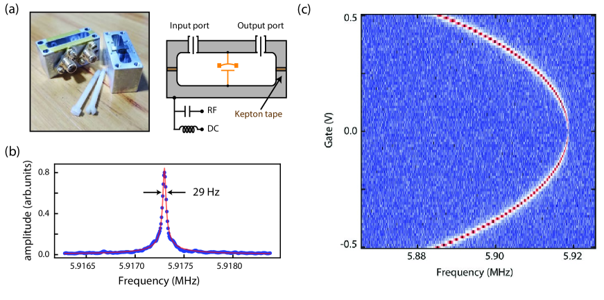
The large capacitance between the two halves of a 3D waveguide cavity naturally offers a low-impedance environment around the electromagnetic mode of the cavity. Based on the physical dimensions of cavity-halves, we estimated a capacitance of 250 pF between them, suggesting a possibility of applying a DC-voltage via the two halves. We introduce a DC voltage in our optomechanical device by electrically isolating the two halves of the cavity by a thin-insulating layer cohen_split-cavity_2017 . A representative image of cavity assembly, along with a schematic of such a device is shown in Fig. 4(a). Electrical isolation obtained between the two parts of the cavity enables the application of a DC voltage across the mechanical capacitor. Further, a low frequency RF signal can be added using a bias tee at low temperatures, facilitating a direct drive of the mechanical resonator given by the force , where and are the amplitudes of RF and DC signals, respectively. For mechanical readout, a microwave tone at is injected into the cavity, and the transmitted signal is then demodulated and recorded at room temperature, while the mechanical resonator is driven by a low frequency RF signal. To reduce any RF-leakage to the output chain, we added two 4-8 GHz bandpass filters before the low noise amplifiers, yielding a 80 dB suppression of low frequency signals. We measured an insertion loss of 34dB between the input microwave port and DC port of the cavity.
On characterization of microwave cavity, the internal linewidth was measured to be MHz. Further details on the cooperativity and single photon coupling strength of this system are provided in the SM. Fig. 4(b) shows the measurements from a device assembled to have a DC-voltage across the mechanical resonator. While directly driving it with a low-frequency RF signal, the mechanical response shows a linewidth of = 29 Hz. The DC voltage allows us to tune the mechanical resonant frequency by electrostatic-pulling. Fig. 4(c) shows the parabolic variation in drum frequency with an applied gate voltage. Such a “negative-dispersion” of resonant frequency with DC gate voltage is well-understood due to capacitive-softening of the effective spring constant of the mechanical resonator kozinsky_tuning_2006 .
VI Conclusions and Outlook
To summarize, we described a scheme to couple nano/micro-mechanical resonators to a waveguide cavity. The design guidelines discussed here, help to minimize the parasitic capacitance, an important criterion to improve single-photon coupling strength. Our design, along with the ability to add a DC voltage can easily be extended to optomechanical systems with novel materials such as graphene, NbSe2, BSCCO, etc to study their intrinsic performance, phase-transitions, or to further improve the single-photon coupling rate, while much simplifying the related nano-fabrication. Looking forward, by reducing the separation between the capacitor plates, we will be able to improve the single-photon coupling rate to 200 Hz for a gap of 60 nm. Together with the large dynamic range of 3D cavities, this would let us perform experiments near the ultra-strong coupling limit, enabling the study of quantum behavior of massive mechanical resonators.
VII Acknowledgments
The authors would like to thank Mandar Deshmukh for providing valuable inputs. This work was supported by the Department of Atomic Energy, under the Young Scientist Research Award. B.G. acknowledges support by the UGC under the D.S. Kothari Fellowship program. The authors acknowledge device fabrication facilities at CeNSE, IISc Bangalore, and central facilities at the Department of Physics funded by DST.
References
- (1) Braginsky, V. B. and Khalili, F. Y. Quantum Measurement. Cambridge University Press, May (1995).
- (2) Aspelmeyer, M., Kippenberg, T. J., and Marquardt, F. Rev. Mod. Phys. 86, 1391–1452 Dec (2014).
- (3) Metcalfe, M. Applied Physics Reviews 1(3), 031105 (2014).
- (4) Brendel, C., Peano, V., Painter, O. J., and Marquardt, F. Proceedings of the National Academy of Sciences 114(17), E3390–E3395 April (2017).
- (5) Teufel, J. D., Donner, T., Li, D., Harlow, J. W., Allman, M. S., Cicak, K., Sirois, A. J., Whittaker, J. D., Lehnert, K. W., and Simmonds, R. W. Nature 475(7356), 359–363 July (2011).
- (6) Chan, J., Alegre, T. P. M., Safavi-Naeini, A. H., Hill, J. T., Krause, A., Gröblacher, S., Aspelmeyer, M., and Painter, O. Nature 478(7367), 89–92 October (2011).
- (7) Reed, A. P., Mayer, K. H., Teufel, J. D., Burkhart, L. D., Pfaff, W., Reagor, M., Sletten, L., Ma, X., Schoelkopf, R. J., Knill, E., and Lehnert, K. W. Nature Physics 13(12), 1163–1167 December (2017).
- (8) Peterson, G., Lecocq, F., Cicak, K., Simmonds, R., Aumentado, J., and Teufel, J. Physical Review X 7(3), 031001 July (2017).
- (9) Bernier, N. R., Tóth, L. D., Koottandavida, A., Ioannou, M. A., Malz, D., Nunnenkamp, A., Feofanov, A. K., and Kippenberg, T. J. Nature Communications 8(1), 604 September (2017).
- (10) Pirkkalainen, J.-M., Cho, S. U., Li, J., Paraoanu, G. S., Hakonen, P. J., and Sillanpää, M. A. Nature 494(7436), 211–215 February (2013).
- (11) Schmidt, P., Schwienbacher, D., Pernpeintner, M., Wulschner, F., Deppe, F., Marx, A., Gross, R., and Huebl, H. Applied Physics Letters 113(15), 152601 October (2018).
- (12) Ockeloen-Korppi, C. F., Damskägg, E., Pirkkalainen, J.-M., Asjad, M., Clerk, A. A., Massel, F., Woolley, M. J., and Sillanpää, M. A. Nature 556(7702), 478–482 April (2018).
- (13) Riedinger, R., Wallucks, A., Marinković, I., Löschnauer, C., Aspelmeyer, M., Hong, S., and Gröblacher, S. Nature 556(7702), 473–477 April (2018).
- (14) Teufel, J. D., Li, D., Allman, M. S., Cicak, K., Sirois, A. J., Whittaker, J. D., and Simmonds, R. W. Nature 471(7337), 204–208 March (2011).
- (15) Suh, J., Weinstein, A. J., Lei, C. U., Wollman, E. E., Steinke, S. K., Meystre, P., Clerk, A. A., and Schwab, K. C. Science 344(6189), 1262–1265 June (2014).
- (16) Andrews, R. W., Peterson, R. W., Purdy, T. P., Cicak, K., Simmonds, R. W., Regal, C. A., and Lehnert, K. W. Nature Physics 10(4), 321–326 April (2014).
- (17) Teufel, J. D., Donner, T., Castellanos-Beltran, M. A., Harlow, J. W., and Lehnert, K. W. Nature Nanotechnology 4(12), 820–823 December (2009).
- (18) Singh, V., Bosman, S., Schneider, B., Blanter, Y. M., Castellanos-Gomez, A., and Steele, G. Nature nanotechnology 9(10), 820 (2014).
- (19) Reagor, M., Paik, H., Catelani, G., Sun, L., Axline, C., Holland, E., Pop, I. M., Masluk, N. A., Brecht, T., Frunzio, L., Devoret, M. H., Glazman, L., and Schoelkopf, R. J. Applied Physics Letters 102(19), 192604 May (2013).
- (20) Paik, H., Schuster, D. I., Bishop, L. S., Kirchmair, G., Catelani, G., Sears, A. P., Johnson, B. R., Reagor, M. J., Frunzio, L., Glazman, L. I., Girvin, S. M., Devoret, M. H., and Schoelkopf, R. J. Physical Review Letters 107(24), 240501 December (2011).
- (21) Menke, T., Burns, P. S., Higginbotham, A. P., Kampel, N. S., Peterson, R. W., Cicak, K., Simmonds, R. W., Regal, C. A., and Lehnert, K. W. Review of Scientific Instruments 88(9), 094701 September (2017).
- (22) Ball, J. R., Yamashiro, Y., Sumiya, H., Onoda, S., Ohshima, T., Isoya, J., Konstantinov, D., and Kubo, Y. Applied Physics Letters 112(20), 204102 May (2018).
- (23) Tabuchi, Y., Ishino, S., Noguchi, A., Ishikawa, T., Yamazaki, R., Usami, K., and Nakamura, Y. Science 349(6246), 405–408 July (2015).
- (24) Yuan, M., Singh, V., Blanter, Y. M., and Steele, G. A. Nature communications 6, 8491 (2015).
- (25) Noguchi, A., Yamazaki, R., Ataka, M., Fujita, H., Tabuchi, Y., Ishikawa, T., Usami, K., and Nakamura, Y. New Journal of Physics 18(10), 103036 (2016).
- (26) Will, M., Hamer, M., Müller, M., Noury, A., Weber, P., Bachtold, A., Gorbachev, R. V., Stampfer, C., and Güttinger, J. Nano Letters 17(10), 5950–5955 October (2017).
- (27) Northeast, D. B. and Knobel, R. G. Materials Research Express 5(3), 035023 (2018).
- (28) Foster, R. M. Bell System Technical Journal 3(2), 259–267 (1924).
- (29) Nigg, S. E., Paik, H., Vlastakis, B., Kirchmair, G., Shankar, S., Frunzio, L., Devoret, M. H., Schoelkopf, R. J., and Girvin, S. M. Physical Review Letters 108(24), 240502 June (2012).
- (30) The supplemental material is available at URL (to be inserted by the publisher).
- (31) Weis, S., Rivière, R., Deléglise, S., Gavartin, E., Arcizet, O., Schliesser, A., and Kippenberg, T. J. Science 330(6010), 1520–1523 December (2010).
- (32) Andrews, R. W., Reed, A. P., Cicak, K., Teufel, J. D., and Lehnert, K. W. Nature Communications 6, 10021 November (2015).
- (33) Chen, F., Sirois, A. J., Simmonds, R. W., and Rimberg, A. J. Applied Physics Letters 98(13), 132509 March (2011).
- (34) Bosman, S. J., Singh, V., Bruno, A., and Steele, G. A. Applied Physics Letters 107(19), 192602 November (2015).
- (35) Cohen, M. A., Yuan, M., de Jong, B. W. A., Beukers, E., Bosman, S. J., and Steele, G. A. Applied Physics Letters 110(17), 172601 April (2017).
- (36) Kozinsky, I., Postma, H. W. C., Bargatin, I., and Roukes, M. L. Applied Physics Letters 88(25), 253101 June (2006).