Hubbard NEGF Analysis of Photocurrent in Nitroazobenzene Molecular Junction
Abstract
We present combined experimental and theoretical study of photo-induced current in molecular junctions consisting of monolayers of nitroazobenzene oligomers chemisorbed on carbon surfaces and illuminated by UV-Vis light through a transparent electrode. Experimentally observed dependence of the photocurrent on light frequency, temperature and monolayer thickness is analyzed within first principles simulations employing the Hubbard NEGF diagrammatic technique. We reproduce qualitatively correct behavior and discuss mechanisms leading to characteristic behavior of dark and photo-induced currents in response to changes in bias, frequency of radiation, temperature and thickness of molecular layer.
keywords:
optoelectronics, photocurrent, molecular junctions, Hubbard NEGFUCSD]Department of Chemistry and Biochemistry, University of California San Diego, La Jolla, CA 92034, USA University of Alberta]Department of Chemistry, University of Alberta, Edmonton, Canada University of Alberta]Department of Chemistry, University of Alberta, Edmonton, Canada \phone+1-858-246-0511 UCSD]Department of Chemistry and Biochemistry, University of California San Diego, La Jolla, CA 92034, USA \abbreviationsNAB, NEGF, DFT
![[Uncaptioned image]](/html/1902.02917/assets/x1.png)
The interaction of light with molecules is an important field of research due to its ability to provide information on molecular structure and dynamics, and to serve as a control tool for intra-molecular processes. Development of nano-fabrication and optical techniques at nanoscale led to tremendous progress in ability to detect and manipulate molecules on surfaces and in junctions. The main signal reported in the literature for devices consisting of molecules attached to macroscopic leads for a long time was current-voltage (conductance-voltage) characteristics 1, 2, 3, 4, 5, 6. Later, standard junction spectroscopies (such as resonant 7, 8 and off-resonant 9, 10, 11, 12, 13 inelastic electron tunneling spectroscopy) were complemented by probing molecular conduction junctions by optical means 14, 15, 16, 17, 18, 19, 20, 21, 22, 23. For single-molecule junctions the latter is possible only by local electromagnetic field enhancement associated with plasmon excitations 24, 25. Recent developments include observation and optical control of current 26, 27, 28 noise 29, 30, and energy transfer 31, 32. Time-dependent and transient effects in junctions observed with optical means 33, 34, 35, 36, tip-enhanced Raman spectroscopy 37, 38, 39, 40, pump-probe spectroscopy in nanojunctions 41, 42, and reporting quantum interference effects 43, 44 are also among recent developments. Optical spectroscopy yields a way to estimate heating in current carrying junction 18, 19, 45, 46 Recently, multidimensional spectroscopy measurements in the presence of current (although not yet in junctions) were reported in the literature.47, 48, 49. Optical effects have been also reported in large-area molecular junctions, including internal photoemission 50, optical modulation of conductance 51, light emission 52, 53, 54, 55, and photocurrents induced by light absorption 56, 57. Experimental capabilities to study radiation field interaction with molecular conducting junctions gave rise to new branch of nanoscale research - molecular optoelectronics 58, 59
Theoretically, challenges in describing optical response in molecular junctions include necessity to account for open character of the system which requires simultaneous treatment of optical transitions in the molecule and electron transfer between molecule and contacts. Single particle language utilized in majority of ab initio studies in molecular electronics usually in the framework of the nonequilibrium Green functions (NEGF) makes it inconvenient to account for differences between transport and optical gaps in junctions. A possible alternative is utilization of molecular many-body states as a basis of consideration. In junctions, such consideration requires utilization of one of many-body flavors of the NEGF. In particular, recently introduced by us diagrammatic technique for the Hubbard NEGF 60 yields a stable and accurate many-body method 61 conveniently suited for description of optoelectronic devices 59.
Here, we apply the methodology to perform first principles simulation of optical response of recently reported large area nitroazobenzene molecular junctions. Illumination by UV-Vis light induces major changes in current-voltage response, with orders of magnitude changes in conductance and distinct bias dependence compared to the dark behavior 56. Below after introducing theoretical model and calculational procedure, we present results of first principles simulations and compare them with corresponding experimental data. We then discuss possible mechanisms for changes in dark and photo-induced currents in response to bias, temperature, light frequency, and thickness of the molecular layer.
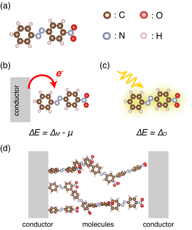
We consider a nitroazobenzene molecule (see Fig. 1a), , bridging two metal electrodes, and , and subjected to an external laser radiation, . The Hamiltonian of the junction is
| (1) |
Here and are respectively Hamiltonians of molecule and baths, and introduces coupling between them. We represent molecular Hamiltonian as a tight-binding chain of molecular units (see Fig. 1d)
| (2) |
For simplicity, we consider all the units to be identical. We represent molecular unit Hamiltonian in terms of many-body states of the unit. In particular, we consider ground, , and excited, , states of neutral molecular unit as well as ground states of anion and cation . First-principle calculations (see Supporting Information for details) yield energies of the states , and explicit form of molecular Hamiltonian is
| (3) |
where is molecule in the chain and is the Hubbard (or projection) operator.
Contacts are modeled as reservoirs of free electrons each at its own equilibrium
| (4) |
and radiation field is described as continuum of modes with one mode corresponding to laser frequency populated while all other modes empty
| (5) |
Here () and () creates (annihilates) electron is state of the contacts and mode of the field, respectively.
Within each molecular unit we consider four electron transitions (see Fig. 1b) , , , and (, , , ) and one optical transition (see Fig. 1c) (). So that, electron transfer between the units is
| (6) |
where are electron transfer transitions in . First molecule of the chain, , is coupled to contact , while last, , couples the chain to contact
| (7) | ||||
| (8) | ||||
| (9) |
Our central object of interest is current through the junction caused by either applied bias (), or laser field, or both - correspondingly, dark, optical, and total fluxes. Current is introduced as rate of change of the population on the contacts, , and at steady-state considered here currents across and junction interfaces are equal (with opposite sign), . Explicit current expression is given by the celebrated Meir-Wingreen formula 62
| (10) |
where trace is over electronic transitions and and are the Fourier transforms of the lesser (greater) projections of electronic self-energy due to coupling to contact and Hubbard Green’s function, respectively. On the Keldysh contour the correlation functions are defined as
| (11) | ||||
| (12) |
Here are the contour variables, is the contour ordering operator, and is the Green’s function for free electron in state .
While explicit expressions for projections of the self-energy are known, Green’s function has to be evaluated by solving a modified Dyson equation on the Keldysh contour. Because the Hubbard GF both depends and defines its self-energies, one has to solve the Dyson equation self-consistently until convergence (see Supporting Information and Refs. 60, 61 for details).
Unless stated otherwise, simulations are performed at temperature K. Ab initio (TD)DFT calculations of an isolated molecular unit yield electronic transitions eV, eV, eV, eV, while optical gap is eV. Strength of molecule-contacts coupling is characterized by escape rate matrix
| (13) |
which within assumed here wide band approximation does not depend on energy. Simulations are performed for eV and eV for and eV and eV for , which are taken to reproduce experimental data (see also Supporting Information). Radiation field is assumed to be coupled to individual molecular units only. Strength of the coupling to radiation field is characterized by dissipation rate
| (14) |
Its frequency dependence is taken from experimental data (see Fig. 2a) with value at molecular resonance, , chosen eV. Fermi energy is taken as an origin, , and bias is applied symmetrically: and . Simulations were performed on energy grid spanning range from to eV with step meV. Convergence was assumed to be reached when populations of the many-body states at subsequent steps of the self-consistent procedure differ by less than .
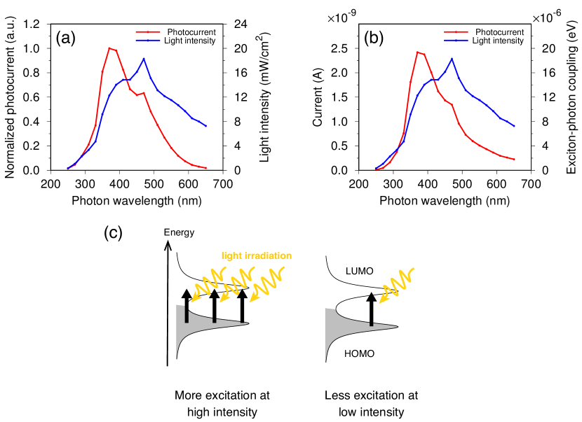
We first consider photo-induced flux in the absence of bias. Here, we employ single molecular unit model, , in the analysis. Optical excitation promotes electronic population from ground to excited state, then electron either relaxes back or escapes into contacts. Asymmetric coupling of excited state leads to appearance of directed flux even in absence of bias. Figure 2 compares experimental data (panel a) with first principles calculation (panel b). Experimental data for light intensity (blue line) was used as an input in the calculations. As expected, photocurrent shows maximum at frequency corresponding to optical transition (panel c). Such light-induced transport was discussed in theoretical literature within simple model considerations 63. Shoulder observed at longer wavelengths is associated with peak in light intensity at this frequency. One sees qualitative correspondence between experimental data and theoretical simulations.
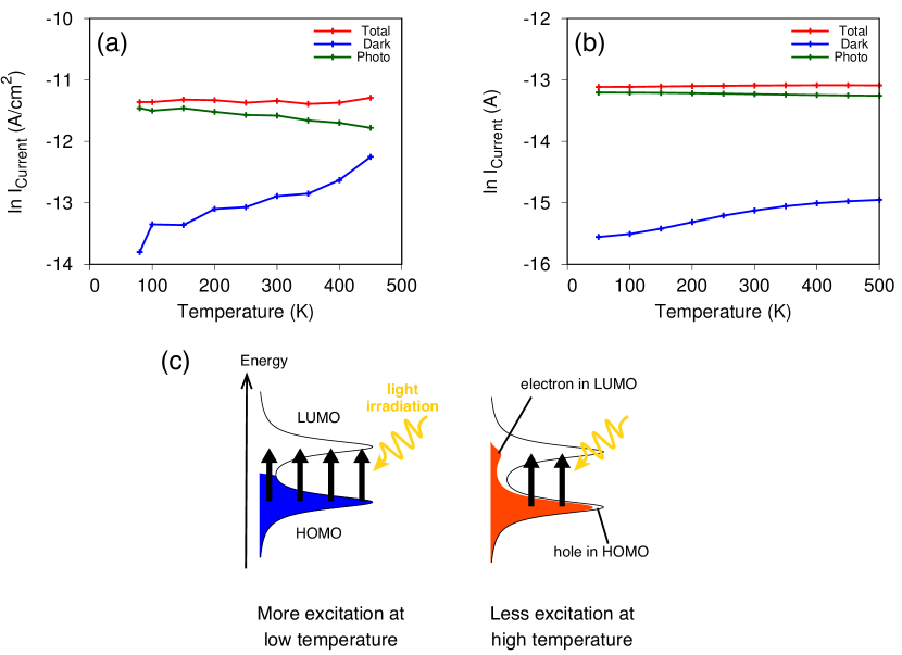
We now turn to consideration of temperature dependence of current. Also here single molecular unit model, , is enough to describe the observed physics Here junction is subjected to bias of eV and measurements are performed in the absence of external radiation (dark current) and under radiation of nm. With temperature increase the experimental data (see Fig. 3a) show an increase in dark current. At the same time, photo-current (defined as difference between total and dark fluxes) decreases. We note that in the experiment dark current is caused by off-resonant tunneling, while radiation transfers electronic population from ground to excited state in near resonance conditions. Thus plausible mechanism can be suggested based on the smearing of Fermi distributions in the contacts with temperature increase. In absence of external radiation extended tail of Fermi distribution at higher temperatures yields more electronic population closer to molecular resonance, which naturally leads to increase of electron flux. On the contrary, optical flux already being at resonance mostly depends on available electronic population at ground state. Smearing of Fermi distribution slightly diminishes the latter thus resulting in decrease of photo-induced current (see Fig. 3c). First principles simulations based on the proposed mechanism (see Fig. 3b) demonstrate qualitative correspondence with experimental data. We note that possible additional factor (not included into the model) decreasing photocurrent with temperature is scattering within the monolayer 56.
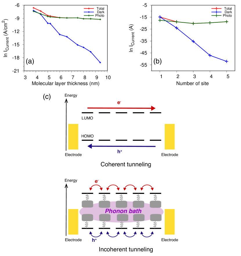
Finally, we consider dependence of photocurrent on thickness of molecular layer. The consideration requires performing calculations for molecular chains of different lengths. In the analysis below we consider chains from to units. While dark current demonstrates exponential dependence on the layer size characteristic of tunneling, photocurrent practically does not depend on the thickness (see Fig. 4a). Such insensitivity is expected for hopping transport, and interplay between the two modes of behavior was discussed in the literature as result of competition between tunneling and thermally activated electron transfer via molecular bridges 64, 65, 66. We suggest that the same mechanism is behind observed length dependence also in transport with a difference that optical excitation in present case plays the role of thermal activation in previous study (see Fig. 4c).
Hopping character of electron transport is caused by local dephasing (e.g., due to interaction with low frequency vibrations of nearby molecules in the layer), which is usually modeled by introducing Buttiker probes. Following Ref. 67 we represent Buttiker probes by attaching set of oscillators to each many-body state of molecules
| (15) |
and considering a limit of to restrict the effect of oscillators to pure dephasing.
We treat both inter-molecule coupling and interactions with Buttiker probes within second order of diagrammatic perturbation theory for the Hubbard NEGF 60. This leads to appearance of two additional self-energies in the self-consistent scheme (see Supporting Information for details). The two interactions are characterized by inter-atomic electron tunneling parameters and dephasing rate
| (16) |
which we consider within wide band approximation. In the simulations all inter-molecule hopping parameters are taken eV, dephasing rates are assumed to be eV.
Figure 4 compares experimental data (panel a) with results of simulation (panel b). Simulations are performed under bias eV and external field illumination at wavelength nm. In both graphs dark current demonstrates exponential dependence on thickness of molecular layer characteristic for off-resonant tunneling through wide barrier. Photocurrent shows insensitivity to barrier width, which is characteristic of hopping transport regime. We note that the inverse Arrhenius behavior for the photocurrent evident in Figure 3a indicates that the hopping is activationless 56.
In summary, we presented combined experimental and theoretical study of response of nitroazobenzene molecular junctions to external illumination and applied bias. Experimentally observed characteristic behavior of dark and photo-induced currents was modeled within new diagrammatic technique for the Hubbard NEGF. Being a nonequilibrum atomic limit tool (i.e. formulation employing many-body states of isolated molecule as a basis) the Hubbard NEGF readily allows incorporation of the results of quantum chemistry simulations into transport behavior. We used first principles simulations to model photocurrent behavior and propose mechanisms behind the observed junction responses. In particular, temperature dependence of the currents is explained by smearing Fermi-Dirac distribution in the contacts with temperature increase, which results in increase of dark current due to shifting electron tunneling energies closer to molecular resonances and decrease of photo-induced current due to diminished population in the ground state. We note that scattering within molecular layer is an additional factor reducing photocurrent, which was not included in the theoretical model. Also, exponential decrease of dark current with molecular layer thickness was explained as a manifestation of (off-resonant) tunneling through a barrier, while insensitivity of photo-induced current on barrier thickness was identified with hopping regime of transport.
Further development of the Hubbard NEGF theory, formulation of universal Hubbard NEGF code for multi-state considerations, and application it to simulation of signals beyond fluxes are goals of future research.
M.G. and K.M. gratefully acknowledge support by the DOE BES (grant DE-SC0018201). R.L.M. and A.M.N acknowledge support from the Natural Science and Engineering Research Council of Canada and Alberta Innovates.
Supporting information contains details on first principle (TD)DFT simulations and short description of the Hubbard NEGF employed in transport modeling.
References
- Aviram and Ratner 1974 Aviram, A.; Ratner, M. A. Molecular rectifiers. Chem. Phys. Lett. 1974, 29, 277–283
- Nitzan and Ratner 2003 Nitzan, A.; Ratner, M. A. Electron Transport in Molecular Wire Junctions. Science 2003, 300, 1384–1389
- Lindsay and Ratner 2007 Lindsay, S. M.; Ratner, M. A. Molecular Transport Junctions: Clearing Mists. Advanced Materials 2007, 19, 23–31
- Tao 2006 Tao, N. J. Electron transport in molecular junctions. Nature Nanotechnology 2006, 1, 173–181
- Galperin et al. 2008 Galperin, M.; Ratner, M. A.; Nitzan, A.; Troisi, A. Nuclear Coupling and Polarization in Molecular Transport Junctions: Beyond Tunneling to Function. Science 2008, 319, 1056–1060
- Galperin et al. 2007 Galperin, M.; Ratner, M. A.; Nitzan, A. Molecular transport junctions: vibrational effects. J. Phys.: Condens. Matter 2007, 19, 103201
- Zhitenev et al. 2002 Zhitenev, N. B.; Meng, H.; Bao, Z. Conductance of Small Molecular Junctions. Phys. Rev. Lett. 2002, 88, 226801
- Dekker 1977 Dekker, H. Quantization of the linearly damped harmonic oscillator. Phys. Rev. A 1977, 16, 2126–2134
- Bayman et al. 1981 Bayman, A.; Hansma, P. K.; Kaska, W. C. Shifts and dips in inelastic-electron-tunneling spectra due to the tunnel-junction environment. Phys. Rev. B 1981, 24, 2449 – 2455
- Hahn et al. 2000 Hahn, J. R.; Lee, H. J.; Ho, W. Electronic Resonance and Symmetry in Single-Molecule Inelastic Electron Tunneling. Phys. Rev. Lett. 2000, 85, 1914 – 1917
- Wang et al. 2004 Wang, W.; Lee, T.; Kretzschmar, I.; Reed, M. A. Inelastic Electron Tunneling Spectroscopy of an Alkanedithiol Self-Assembled Monolayer. Nano Lett. 2004, 4, 643–646
- Smit et al. 2002 Smit, R. H. M.; Noat, Y.; Untiedt, C.; Lang, N. D.; van Hemert, M. C.; van Ruitenbeek, J. M. Measurement of the conductance of a hydrogen molecule. Nature 2002, 419, 906–909
- Agrait et al. 2002 Agrait, N.; Untiedt, C.; Rubio-Bollinger, G.; Vieira, S. Onset of Energy Dissipation in Ballistic Atomic Wires. Phys. Rev. Lett. 2002, 88, 216803
- Zhang et al. 2007 Zhang, J.; Fu, Y.; Chowdhury, M. H.; Lakowicz, J. R. Metal-Enhanced Single-Molecule Fluorescence on Silver Particle Monomer and Dimer: Coupling Effect between Metal Particles. Nano Lett. 2007, 7, 2101–2107
- Wu et al. 2008 Wu, S. W.; Nazin, G. V.; Ho, W. Intramolecular photon emission from a single molecule in a scanning tunneling microscope. Phys. Rev. B 2008, 77, 205430
- Yoon et al. 2010 Yoon, H. P.; Maitani, M. M.; Cabarcos, O. M.; Cai, L.; Mayer, T. S.; Allara, D. L. Crossed-Nanowire Molecular Junctions: A New Multispectroscopy Platform for Conduction-Structure Correlations. Nano Lett. 2010, 10, 2897–2902
- Ward et al. 2008 Ward, D. R.; Halas, N. J.; Ciszek, J. W.; Tour, J. M.; Wu, Y.; Nordlander, P.; Natelson, D. Simultaneous Measurements of Electronic Conduction and Raman Response in Molecular Junctions. Nano Lett. 2008, 8, 919–924
- Ioffe et al. 2008 Ioffe, Z.; Shamai, T.; Ophir, A.; Noy, G.; Yutsis, I.; Kfir, K.; Cheshnovsky, O.; Selzer, Y. Detection of heating in current-carrying molecular junctions by Raman scattering. Nature Nanotech. 2008, 3, 727–732
- Ward et al. 2011 Ward, D. R.; Corley, D. A.; Tour, J. M.; Natelson, D. Vibrational and electronic heating in nanoscale junctions. Nature Nanotech. 2011, 6, 33–38
- Kim et al. 2011 Kim, K.; Choi, J.-Y.; Lee, H. B.; Shin, K. S. Raman scattering of 4-aminobenzenethiol sandwiched between Ag nanoparticle and macroscopically smooth Au substrate: Effects of size of Ag nanoparticles and the excitation wavelength. The Journal of Chemical Physics 2011, 135, 124705
- Shamai and Selzer 2011 Shamai, T.; Selzer, Y. Spectroscopy of molecular junctions. Chem. Soc. Rev. 2011, 40, 2293–2305
- Banik et al. 2012 Banik, M.; El-Khoury, P. Z.; Nag, A.; Rodriguez-Perez, A.; Guarrottxena, N.; Bazan, G. C.; Apkarian, V. A. Surface-Enhanced Raman Trajectories on a Nano-Dumbbell: Transition from Field to Charge Transfer Plasmons as the Spheres Fuse. ACS Nano 2012, 6, 10343–10354
- Zhang et al. 2013 Zhang, R.; Zhang, Y.; Dong, Z. C.; Jiang, S.; Zhang, C.; Chen, L. G.; Zhang, L.; Liao, Y.; Aizpurua, J.; Luo, Y.; Yang, J. L.; Hou, J. G. Chemical mapping of a single molecule by plasmon-enhanced Raman scattering. Nature 2013, 498, 82–86
- Ward et al. 2007 Ward, D. R.; Grady, N. K.; Levin, C. S.; Halas, N. J.; Wu, Y.; Nordlander, P.; Natelson, D. Electromigrated Nanoscale Gaps for Surface-Enhanced Raman Spectroscopy. Nano Lett. 2007, 7, 1396–1400
- Arielly et al. 2011 Arielly, R.; Ofarim, A.; Noy, G.; Selzer, Y. Accurate Determination of Plasmonic Fields in Molecular Junctions by Current Rectification at Optical Frequencies. Nano Lett. 2011, 11, 2968–2972
- Vadai et al. 2013 Vadai, M.; Nachman, N.; Ben-Zion, M.; Bürkle, M.; Pauly, F.; Cuevas, J. C.; Selzer, Y. Plasmon-Induced Conductance Enhancement in Single-Molecule Junctions. J. Phys. Chem. Lett. 2013, 4, 2811–2816
- Dey et al. 2013 Dey, S.; Mirell, D.; Perez, A. R.; Lee, J.; Apkarian, V. A. Nonlinear femtosecond laser induced scanning tunneling microscopy. The Journal of Chemical Physics 2013, 138, –
- Evans et al. 2015 Evans, K. M.; Zolotavin, P.; Natelson, D. Plasmon-Assisted Photoresponse in Ge-Coated Bowtie Nanojunctions. ACS Photonics 2015, 2, 1192–1198
- Schneider et al. 2010 Schneider, N. L.; Schull, G.; Berndt, R. Optical Probe of Quantum Shot-Noise Reduction at a Single-Atom Contact. Phys. Rev. Lett. 2010, 105, 026601
- Schneider et al. 2012 Schneider, N. L.; Lü, J. T.; Brandbyge, M.; Berndt, R. Light Emission Probing Quantum Shot Noise and Charge Fluctuations at a Biased Molecular Junction. Phys. Rev. Lett. 2012, 109, 186601
- Imada et al. 2016 Imada, H.; Miwa, K.; Imai-Imada, M.; Kawahara, S.; Kimura, K.; Kim, Y. Real-space investigation of energy transfer in heterogeneous molecular dimers. Nature 2016, 538, 364–367
- Imada et al. 2017 Imada, H.; Miwa, K.; Imai-Imada, M.; Kawahara, S.; Kimura, K.; Kim, Y. Single-Molecule Investigation of Energy Dynamics in a Coupled Plasmon-Exciton System. Phys. Rev. Lett. 2017, 119, 013901
- Sonntag et al. 2013 Sonntag, M. D.; Chulhai, D.; Seideman, T.; Jensen, L.; Duyne, R. P. V. The Origin of Relative Intensity Fluctuations in Single-Molecule Tip-Enhanced Raman Spectroscopy. Journal of the American Chemical Society 2013, 135, 17187–17192
- El-Khoury et al. 2013 El-Khoury, P. Z.; Hu, D.; Apkarian, V. A.; Hess, W. P. Raman Scattering at Plasmonic Junctions Shorted by Conductive Molecular Bridges. Nano Letters 2013, 13, 1858–1861
- Yampolsky et al. 2014 Yampolsky, S.; Fishman, D. A.; Dey, S.; Hulkko, E.; Banik, M.; Potma, E. O.; Apkarian, V. A. Seeing a single molecule vibrate through time-resolved coherent anti-Stokes Raman scattering. Nat. Photon. 2014, 8, 650–656
- Arielly et al. 2014 Arielly, R.; Vadai, M.; Kardash, D.; Noy, G.; Selzer, Y. Real-Time Detection of Redox Events in Molecular Junctions. Journal of the American Chemical Society 2014, 136, 2674–2680
- Pozzi et al. 2013 Pozzi, E. A.; Sonntag, M. D.; Jiang, N.; Klingsporn, J. M.; Hersam, M. C.; Duyne, R. P. V. Tip-Enhanced Raman Imaging: An Emergent Tool for Probing Biology at the Nanoscale. ACS Nano 2013, 7, 885–888
- Klingsporn et al. 2014 Klingsporn, J. M.; Sonntag, M. D.; Seideman, T.; Van Duyne, R. P. Tip-Enhanced Raman Spectroscopy with Picosecond Pulses. J. Phys. Chem. Lett. 2014, 5, 106–110, PMID: 26276188
- Pozzi et al. 2014 Pozzi, E. A.; Sonntag, M. D.; Jiang, N.; Chiang, N.; Seideman, T.; Hersam, M. C.; Duyne, R. P. V. Ultrahigh Vacuum Tip-Enhanced Raman Spectroscopy with Picosecond Excitation. The Journal of Physical Chemistry Letters 2014, 5, 2657–2661
- Kurouski et al. 2015 Kurouski, D.; Mattei, M.; Van Duyne, R. P. Probing Redox Reactions at the Nanoscale with Electrochemical Tip-Enhanced Raman Spectroscopy. Nano Lett. 2015, 15, 7956–7962, PMID: 26580153
- Grosse et al. 2013 Grosse, C.; Etzkorn, M.; Kuhnke, K.; Loth, S.; Kern, K. Quantitative mapping of fast voltage pulses in tunnel junctions by plasmonic luminescence. Appl. Phys. Lett. 2013, 103, 183108
- Jahng et al. 2015 Jahng, J.; Brocious, J.; Fishman, D. A.; Yampolsky, S.; Nowak, D.; Huang, F.; Apkarian, V. A.; Wickramasinghe, H. K.; Potma, E. O. Ultrafast pump-probe force microscopy with nanoscale resolution. Applied Physics Letters 2015, 106, –
- Jiang et al. 2012 Jiang, N.; Foley, E. T.; Klingsporn, J. M.; Sonntag, M. D.; Valley, N. A.; Dieringer, J. A.; Seideman, T.; Schatz, G. C.; Hersam, M. C.; Van Duyne, R. P. Observation of Multiple Vibrational Modes in Ultrahigh Vacuum Tip-Enhanced Raman Spectroscopy Combined with Molecular-Resolution Scanning Tunneling Microscopy. Nano Lett. 2012, 12, 5061–5067, PMID: 22200250
- Lee et al. 2014 Lee, J.; Perdue, S. M.; Perez, A. R.; Apkarian, V. A. Vibronic Motion with Joint Angstrom-Femtosecond Resolution Observed through Fano Progressions Recorded within One Molecule. ACS Nano 2014, 8, 54–63, PMID: 24261832
- Herzog et al. 2014 Herzog, J. B.; Knight, M. W.; Natelson, D. Thermoplasmonics: Quantifying Plasmonic Heating in Single Nanowires. Nano Letters 2014, 14, 499–503
- Pozzi et al. 2015 Pozzi, E. A.; Zrimsek, A. B.; Lethiec, C. M.; Schatz, G. C.; Hersam, M. C.; Van Duyne, R. P. Evaluating Single-Molecule Stokes and Anti-Stokes SERS for Nanoscale Thermometry. J. Phys. Chem. C 2015, 119, 21116–21124
- Nardin et al. 2013 Nardin, G.; Autry, T. M.; Silverman, K. L.; Cundiff, S. T. Multidimensional coherent photocurrent spectroscopy of a semiconductor nanostructure. Opt. Express 2013, 21, 28617–28627
- Karki et al. 2014 Karki, K. J.; Widom, J. R.; Seibt, J.; Moody, I.; Lonergan, M. C.; Pullerits, T.; Marcus, A. H. Coherent two-dimensional photocurrent spectroscopy in a PbS quantum dot photocell. Nat. Commun. 2014, 5, 5869
- Vella et al. 2016 Vella, E.; Li, H.; Grégoire, P.; Tuladhar, S. M.; Vezie, M. S.; Few, S.; Bazán, C. M.; Nelson, J.; Silva-Acuña, C.; Bittner, E. R. Ultrafast decoherence dynamics govern photocarrier generation efficiencies in polymer solar cells. Sci. Rep. 2016, 6, 29437–
- Fereiro et al. 2015 Fereiro, J. A.; Kondratenko, M.; Bergren, A. J.; McCreery, R. L. Internal Photoemission in Molecular Junctions: Parameters for Interfacial Barrier Determinations. J. Am. Chem. Soc. 2015, 137, 1296–1304, PMID: 25562564
- Pourhossein et al. 2016 Pourhossein, P.; Vijayaraghavan, R. K.; Meskers, S. C. J.; Chiechi, R. C. Optical modulation of nano-gap tunnelling junctions comprising self-assembled monolayers of hemicyanine dyes. Nat. Commun. 2016, 7, 11749
- Ivashenko et al. 2016 Ivashenko, O.; Bergren, A. J.; McCreery, R. L. Monitoring of Energy Conservation and Losses in Molecular Junctions through Characterization of Light Emission. Adv. Electron. Mater. 2016, 2, 1600351
- Ivashenko et al. 2016 Ivashenko, O.; Bergren, A. J.; McCreery, R. L. Light Emission as a Probe of Energy Losses in Molecular Junctions. J. Am. Chem. Soc. 2016, 138, 722–725, PMID: 26745544
- Du et al. 2016 Du, W.; Wang, T.; Chu, H.-S.; Wu, L.; Liu, R.; Sun, S.; Phua, W. K.; Wang, L.; Tomczak, N.; Nijhuis, C. A. On-chip molecular electronic plasmon sources based on self-assembled monolayer tunnel junctions. Nat. Photon. 2016, 10, 274–280
- Tefashe et al. 2017 Tefashe, U. M.; Nguyen, Q. V.; Lafolet, F.; Lacroix, J.-C.; McCreery, R. L. Robust Bipolar Light Emission and Charge Transport in Symmetric Molecular Junctions. J. Am. Chem. Soc. 2017, 139, 7436–7439, PMID: 28528551
- Najarian and McCreery 2019 Najarian, A. M.; McCreery, R. L. Long-Range Activationless Photostimulated Charge Transport in Symmetric Molecular Junctions. ACS Nano 2019, 13, 867–877
- Morteza Najarian et al. 2018 Morteza Najarian, A.; Bayat, A.; McCreery, R. L. Orbital Control of Photocurrents in Large Area All-Carbon Molecular Junctions. J. Am. Chem. Soc. 2018, 140, 1900–1909, PMID: 29319313
- Galperin and Nitzan 2012 Galperin, M.; Nitzan, A. Molecular optoelectronics: The interaction of molecular conduction junctions with light. Phys. Chem. Chem. Phys. 2012, 14, 9421–9438
- Galperin 2017 Galperin, M. Photonics and spectroscopy in nanojunctions: a theoretical insight. Chem. Soc. Rev. 2017, 46, 4000–4019
- Chen et al. 2017 Chen, F.; Ochoa, M. A.; Galperin, M. Nonequilibrium diagrammatic technique for Hubbard Green functions. J. Chem. Phys. 2017, 146, 092301
- Miwa et al. 2017 Miwa, K.; Chen, F.; Galperin, M. Towards Noise Simulation in Interacting Nonequilibrium Systems Strongly Coupled to Baths. Scientific Reports 2017, 7, 9735
- Haug and Jauho 2008 Haug, H.; Jauho, A.-P. Quantum Kinetics in Transport and Optics of Semiconductors, second, substantially revised edition ed.; Springer: Berlin Heidelberg, 2008
- Galperin and Nitzan 2005 Galperin, M.; Nitzan, A. Current-Induced Light Emission and Light-Induced Current in Molecular-Tunneling Junctions. Phys. Rev. Lett. 2005, 95, 206802
- Segal et al. 2000 Segal, D.; Nitzan, A.; Davis, W. B.; Wasielewski, M. R.; Ratner, M. A. Electron Transfer Rates in Bridged Molecular Systems 2. A Steady-State Analysis of Coherent Tunneling and Thermal Transitions. 2000, 104, 3817–3829
- Ho Choi et al. 2008 Ho Choi, S.; Kim, B.; Frisbie, C. D. Electrical Resistance of Long Conjugated Molecular Wires. Science 2008, 320, 1482–1486
- Choi et al. 2010 Choi, S. H.; Risko, C.; Delgado, M. C. R.; Kim, B.; Brédas, J.-L.; Frisbie, C. D. Transition from Tunneling to Hopping Transport in Long, Conjugated Oligo-imine Wires Connected to Metals. Journal of the American Chemical Society 2010, 132, 4358–4368, PMID: 20218660
- White et al. 2013 White, A. J.; Peskin, U.; Galperin, M. Coherence in charge and energy transfer in molecular junctions. Phys. Rev. B 2013, 88, 205424