Probing magnetism in 2D materials at the nanoscale with single spin microscopy
The recent discovery of ferromagnetism in 2D van der Waals (vdW) crystals has generated widespread interest, owing to their potential for fundamental and applied research. Advancing the understanding and applications of vdW magnets requires methods to quantitatively probe their magnetic properties on the nanoscale. Here, we report the study of atomically thin crystals of the vdW magnet CrI3 down to individual monolayers using scanning single-spin magnetometry, and demonstrate quantitative, nanoscale imaging of magnetisation, localised defects and magnetic domains. We determine the magnetisation of CrI3 monolayers to be nm2 and find comparable values in samples with odd numbers of layers, whereas the magnetisation vanishes when the number of layers is even. We also establish that this inscrutable even-odd effect is intimately connected to the material structure, and that structural modifications can induce switching between ferro- and anti-ferromagnetic interlayer ordering. Besides revealing new aspects of magnetism in atomically thin CrI3 crystals, these results demonstrate the power of single-spin scanning magnetometry for the study of magnetism in 2D vdW magnets.
Magnetism in individual monolayers of vdW crystals has recently been observed in a range of materials, including semiconducting Huang et al. (2017); Gong et al. (2017) and metallic Bonilla et al. (2018); Fei et al. (2018); Deng et al. (2018) compounds. The discovery of such two dimensional magnetic order is per se non-trivial Mermin and Wagner (1966) and has triggered significant attention owing to emerging exotic phenomena including Kitaev spin liquids Banerjee et al. (2016, 2017), or novel magneto-electric effects Wang et al. (2018a); Jiang et al. (2018a, b); Huang et al. (2018). Remarkable efforts have led to the use of two-dimensional magnets as functional elements in spintronics, such as spin-filters Song et al. (2018); Klein et al. (2018), spin-transistors Jiang et al. (2018c), tunnelling magnetoresistance devices Wang et al. (2018b); Kim et al. (2018) or magneto-electric switches Jiang et al. (2018a, b); Huang et al. (2018). Further advances hinge on methods for the quantitative study of the magnetic response of these atomically thin crystals at the nanoscale, but despite their central importance, the required experimental methods are still lacking. Indeed, transport experiments Song et al. (2018); Jiang et al. (2018c); Klein et al. (2018); Wang et al. (2018b); Jiang et al. (2018a, b) probe magnetic properties only indirectly. The only existing, spatially resolved studies rely on optical techniques, such as fluorescence Zhong et al. (2017); Seyler et al. (2018) or the magneto-optical Kerr effect (MOKE) Huang et al. (2017); Gong et al. (2017); Fei et al. (2018), and are therefore limited to the micron-scale. Even more critically, these techniques do not provide quantitative information about the magnetisation (MOKE, e.g., may yield non-zero signals even for antiferromagnets Sivadas et al. (2016)) and are susceptible to interference effects that can obscure magnetic signals in thin samples Huang et al. (2017).
In this work, we overcome these limitations and present a powerful approach for quantitative addressing of nanoscale magnetic properties of vdW magnets, which we here illustrate on the prominent case of CrI3. Specifically, we employ a scanning Nitrogen-Vacancy (NV) centre spin in diamond as a sensitive, atomic-scale magnetometer Rondin et al. (2014) to quantitatively determine key magnetic properties of CrI3 and to directly image magnetic domains with spatial resolutions of few tens of nanometres. For magnetometry, we exploit the Zeeman effect, which leads to a shift of the NV spin’s energy levels as a function of magnetic field. In the regime relevant for this work, the NV spin shows a linear Zeeman response for magnetic fields along its spin-quantisation axis (Fig. 1A), while it is largely insensitive to fields orthogonal to Rondin et al. (2014). The NV spin therefore offers a direct and quantitative measurement of the vectorial component of stray magnetic fields emerging from a sample.
The Zeeman shifts of the involved NV spin-levels can be conveniently read out by optically detected electron spin resonance (ODMR) using nm laser excitation, microwave spin driving and NV fluorescence detection for spin readout Gruber et al. (1997); SOM . For nanoscale imaging, we employ a single NV spin held in the tip of an atomic force microscope and approach the NV to within a distance nm to the sample, which then results in a magnetic imaging resolution on the order of Rondin et al. (2014). The scanning probe containing the NV Maletinsky et al. (2012); Appel et al. (2016) is integrated into a confocal optical microscope for optical spin readout and the whole apparatus immersed in a liquid-4He cryostat. Superconducting magnets are used to enable vectorial magnetic field control up to T. The measurement temperature of K was determined by a resistive thermometer placed close to the sample.
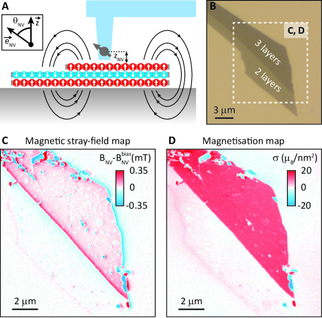
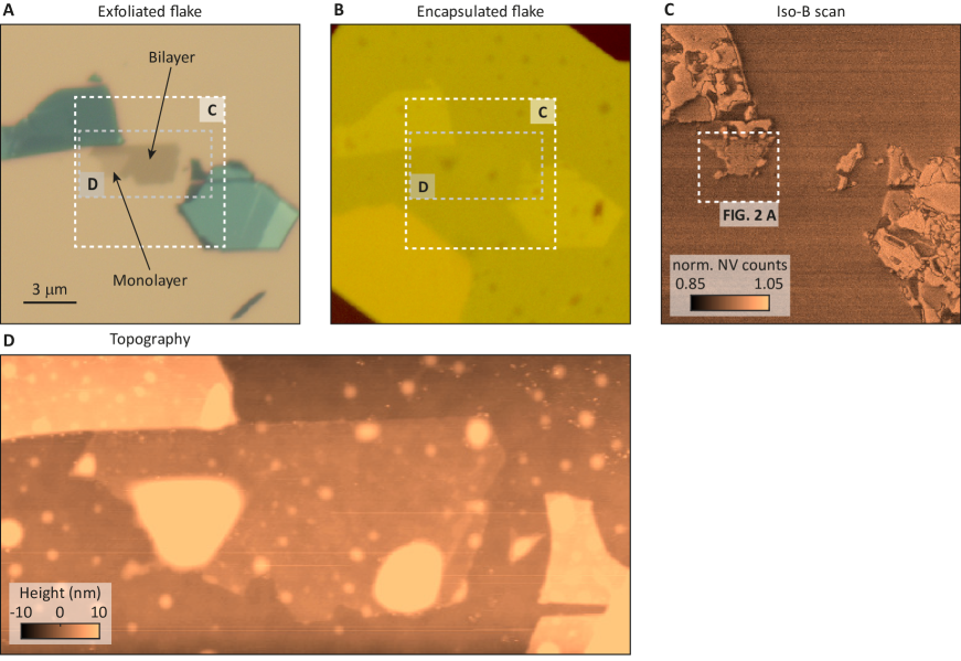
We studied CrI3 samples of various thicknesses, which were encapsulated in either h-BN or graphene to assure the stability of CrI3 under oxygen atmosphere (for details, see SOM ). The samples (Fig. 1B) were fabricated by mechanical exfoliation of CrI3 and subsequently encapsulated using an established pick-and-place technique described elsewhere Wang et al. (2018b). Samples of various CrI3 thicknesses in the range of few () layers were produced to study the effect of thickness on magnetic ordering. For each CrI3 sample, the number of atomic layers was determined by a combination of AFM and optical microscopy SOM . To prepare and study the magnetic state of CrI3, the samples were mounted in the NV magnetometer and cooled in zero magnetic field to the final measurement temperature.
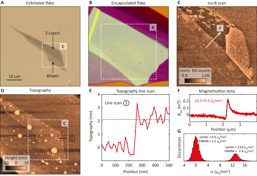
Figure 1C shows a typical magnetic field map we acquired on an area containing bilayer and trilayer CrI3 (sample D1). The presented data were acquired in a bias field mT, where magnetometer performance was optimal, but equivalent images and results were found at lower fields as well. We obtained such maps from NV ODMR spectra acquired at each pixel (acquisition time s/pixel), from which we determined through a fit SOM . We confirmed experimentally that for typical experimental parameters we employed, our approach induced no significant back-action onto the sample, e.g., through heating by laser illumination or microwave irradiation SOM . The resulting data show stray magnetic fields emerging predominantly from the edges of the tri-layer flake, as expected for a largely uniform magnetisation Hingant et al. (2015), and thereby provide clear evidence for the magnetisation of few-layer CrI3 we seek to study.
To reveal further details of the underlying magnetisation pattern in CrI3, we use well-established reverse propagation protocols Roth et al. (1989) to map the magnetic field image of to its source (see SOM for details). For a two-dimensional, out-of-plane magnetisation, as in the present case, such reverse propagation yields a unique determination of the underlying magnetisation pattern (Fig. 1D), provided that the distance between sensor and sample is known. In our refined reverse propagation protocol, we determine through an iterative procedure described elsewhere Appel et al. (2018); SOM . The reverse propagation thereby additionally yields the spatial resolution of our images, which is directly given by (for the data in Fig. 1, nm). In the following, we will focus our discussion on magnetisation maps obtained through such reverse propagation, while the raw magnetic field images are presented in SOM .
The magnetisation pattern in Fig. 1D clearly shows a largely homogenous magnetisation for this trilayer CrI3 flake, which is typical for most samples we investigated. In addition, sparsely scattered, localised defects, mostly with vanishing magnetisation, were visible across the flake and few irregularities occured at the flake edges, which are likely caused by curling and rippling induced on the edges during sample preparation. On the flake, we found an average magnetisation nm2 (with the Bohr magneton), consistent with a single layer of fully polarised Cr+3 spins, for which nm2 would be expected McGuire et al. (2015). The data thus supports the notion of antiferromagnetic interlayer exchange coupling in few-layer CrI3 Huang et al. (2017), which results in a net magnetisation for the magnetically ordered trilayer sample.
Sample D1 additionally contained a region of bilayer CrI3 for which we observed zero bulk moment, again consistent with antiferromagnetic interlayer coupling. However, the bilayer also showed a weak magnetisation located within less than our spatial resolution of its edge (Fig. 1D). The origin of this magnetisation is currently unknown, but could be related to magneto-electric effects Wang et al. (2018a); Jiang et al. (2018b), a narrow region of monolayer CrI3 protruding from the bilayer, or to spin canting Garcia-Sanchez et al. (2014) close to the edge of the flake.
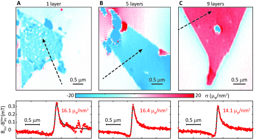
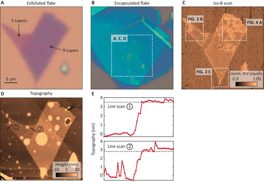
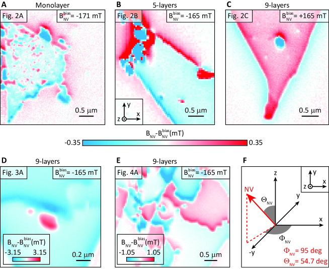
We applied our measurement procedure to a variety of samples, including a monolayer and the 5- and 9-layer flakes shown in Fig. 2A, B and C, respectively. Strikingly, all these flakes exhibit near-uniform magnetisation at a magnitude comparable to . We additionally determined in an independent way by measuring along lines crossing the edges of each flake (Fig. 2, lower panels). Assuming a purely out-of-plane magnetisation, analytical fits Hingant et al. (2015) to these data allow for the quantitative determination of both and . Potential rotations of the magnetisation away from in the vicinity of the edge due to, e.g. the Dzyaloshinskii-Moriya interaction, would only lead to negligible deviations from our findings Tetienne et al. (2015). For the monolayer, 5-, and 9-layer flakes, we then find nm2, nm2 and nm2, respectively, where uncertainties denote statistical errors of the fit (nm in all cases, see SOM ). The general agreement of these fits with the values of found in Fig 2A, B and C further confirms the validity of the reverse propagation method we employed.
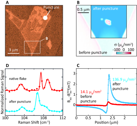
Our observations thus far corroborate previous results on few-layer CrI3 Huang et al. (2018); Seyler et al. (2018); Song et al. (2018), which all found CrI3 flakes with odd (even) numbers of layers to exhibit non-zero (close to zero) magnetisation as a result of antiferromagnetic interlayer exchange coupling. These observations, however, are in conflict with the established fact that CrI3 is a bulk ferromagnet Dillon and Olson (1965). We shed light on this dichotomy in a subsequent experiment on sample D2, where our diamond scanning probe induced an unintentional local puncture through the encapsulation layer of the CrI3 flake (Fig. 3A and SOM ). After this, the whole sample, up to several microns away from the puncture, exhibited a significantly enhanced magnetisation, as evidenced by a representative magnetisation map (Fig. 3B) and linescan (Fig. 3C) across the flake. The data show a -fold increase of magnetisation from initially nm2 to nm2. For the 9-layer flake under study, this enhancement suggests a transition from antiferromagnetic to ferromagnetic interlayer coupling induced by the puncture.
To investigate the occurrence of a structural transition in our punctured sample we have compared in Fig. 3D its low-temperature Raman spectrum with the one of a pristine flake, in a spectral region where characteristic Raman modes for CrI3 exist Djurdjić-Mijin et al. (2018). Although the data does not allow for an unambiguous determination of the crystalline structure of our samples, the markedly different spectra clearly point to a change in structure occurring simultaneously with the change in magnetic order discussed above. This observation is consistent with recent results of density functional calculations Jiang et al. (2018d); Soriano et al. (2018); Sivadas et al. (2018); Jang et al. (2018); Wang et al. (2018b), predicting an interplay between stacking order and interlayer exchange coupling in CrI3. The nature of the structural transition induced by the puncture and the crystalline structure prior to the puncture of the flake need to be elucidated and will be the subject to further research.
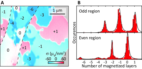
The connection between crystal structure and magnetism also offers an explanation for the occurrence of magnetic domains in some of our CrI3 samples. Figure 4A shows a representative image of such domains on sample D2 (9-layer flake). Strikingly, the measured domain magnetisations only assume values close to integer multiples of , i.e. , with . This observation can be explained by spatial variations (in all three dimensions) of exchange couplings, which may alter the ordering of pairs of CrI3 layers from antiferromagnetic to ferromagnetic between adjacent domains, e.g. due to a local change in crystal structure or stacking order. While this domain formation mechanism would preserve the parity of , we observe well-separated regions on the sample where is either even or odd (see outlines in Fig. 4A and histogram in Fig. 4B). The removal or addition of a monolayer of CrI3 between these areas can explain this observation and could have occurred during material exfoliation or sample preparation.
We have employed scanning NV magnetometry to observe a direct connection between structural and nanoscale magnetic ordering in CrI3, and thereby address the key question of why few-layer CrI3 shows antiferromagnetic interlayer exchange coupling despite the bulk being ferromagnetic. Beyond CrI3, our work establishes scanning NV magnetometry as a unique tool to address nanoscale magnetism in vdW crystals, down to the limit of a single atomic layer. Such direct, quantitative imaging and sensing is vital to further our fundamental understanding of these materials and their development towards applications in future spintronics devices Bonilla et al. (2018); Deng et al. (2018). Our approach is general and can even be applied under ambient conditions Rondin et al. (2014); Bonilla et al. (2018) or to materials where optical methods could not be applied thus far Ghazaryan et al. (2018). Finally, the ability to perform NV magnetometry on vdW magnets offers perspectives for high-frequency sensing Du et al. (2017) of their magnonic excitations Ghazaryan et al. (2018); Klein et al. (2018), and thereby develop vdW magnets towards novel, atomic-scale platforms in magnonics applications.
I Acknowledgements
We thank A. Högele, M. Munsch, and J.-V. Kim for fruitful discussions and valuable feedback on the manuscript and A. Ferreira for technical help. We gratefully acknowledge financial support from the SNI; NCCR QSIT; SNF grants 143697, 155845, 169016 and 178891 the EU Graphene Flagship. N.U. and M.G. gratefully acknowledge support through an Ambizione fellowship of the Swiss National Science Foundation.
II Author contributions
All authors contributed to all aspects of this work.
III Additional information
The authors declare no competing financial interest.
References
- (1) “See supplemental material for additional information,” .
- Hingant et al. (2015) T. Hingant, J.-P. Tetienne, L. J. Martínez, K. Garcia, D. Ravelosona, J.-F. Roch, and V. Jacques, Phys. Rev. Applied 4, 014003 (2015).
- Huang et al. (2017) B. Huang, G. Clark, E. Navarro-Moratalla, D. R. Klein, R. Cheng, K. L. Seyler, D. Zhong, E. Schmidgall, M. A. McGuire, D. H. Cobden, W. Yao, D. Xiao, P. Jarillo-Herrero, and X. Xu, Nature 546, 270 (2017).
- Gong et al. (2017) C. Gong, L. Li, Z. Li, H. Ji, A. Stern, Y. Xia, T. Cao, W. Bao, C. Wang, Y. Wang, Z. Q. Qiu, R. J. Cava, S. G. Louie, J. Xia, and X. Zhang, Nature 546, 265 (2017).
- Bonilla et al. (2018) M. Bonilla, S. Kolekar, Y. Ma, H. C. Diaz, V. Kalappattil, R. Das, T. Eggers, H. R. Gutierrez, M.-H. Phan, and M. Batzill, Nature Nanotechnology 13, 289 (2018).
- Fei et al. (2018) Z. Fei, B. Huang, P. Malinowski, W. Wang, T. Song, J. Sanchez, W. Yao, D. Xiao, X. Zhu, A. F. May, et al., Nature Materials 17, 778 (2018).
- Deng et al. (2018) Y. Deng, Y. Yu, Y. Song, J. Zhang, N. Z. Wang, Y. Z. Wu, J. Zhu, J. Wang, X. H. Chen, and Y. Zhang, arXiv preprint arXiv:1803.02038 (2018).
- Mermin and Wagner (1966) N. D. Mermin and H. Wagner, Phys. Rev. Lett. 17, 1133 (1966).
- Banerjee et al. (2016) A. Banerjee, C. A. Bridges, J. Q. Yan, A. A. Aczel, L. Li, M. B. Stone, G. E. Granroth, M. D. Lumsden, Y. Yiu, J. Knolle, S. Bhattacharjee, D. L. Kovrizhin, R. Moessner, D. A. Tennant, D. G. Mandrus, and S. E. Nagler, Nature Materials 15, 733 (2016).
- Banerjee et al. (2017) A. Banerjee, J. Yan, J. Knolle, C. A. Bridges, M. B. Stone, M. D. Lumsden, D. G. Mandrus, D. A. Tennant, R. Moessner, and S. E. Nagler, Science 356, 1055 (2017).
- Wang et al. (2018a) Z. Wang, T. Zhang, M. Ding, B. Dong, Y. Li, M. Chen, X. Li, J. Huang, H. Wang, X. Zhao, Y. Li, D. Li, C. Jia, L. Sun, H. Guo, Y. Ye, D. Sun, Y. Chen, T. Yang, J. Zhang, S. Ono, Z. Han, and Z. Zhang, Nature Nanotechnology 13, 554 (2018a).
- Jiang et al. (2018a) S. Jiang, J. Shan, and K. F. Mak, Nature Materials 17, 406 (2018a).
- Jiang et al. (2018b) S. Jiang, L. Li, Z. Wang, K. F. Mak, and J. Shan, Nature Nanotechnology 13, 549 (2018b).
- Huang et al. (2018) B. Huang, G. Clark, D. R. Klein, D. MacNeill, E. Navarro-Moratalla, K. L. Seyler, N. Wilson, M. A. McGuire, D. H. Cobden, D. Xiao, W. Yao, P. Jarillo-Herrero, and X. Xu, Nature Nanotechnology 13, 544 (2018).
- Song et al. (2018) T. Song, X. Cai, M. W.-Y. Tu, X. Zhang, B. Huang, N. P. Wilson, K. L. Seyler, L. Zhu, T. Taniguchi, K. Watanabe, M. A. McGuire, D. H. Cobden, D. Xiao, W. Yao, and X. Xu, Science 360, 1214 (2018).
- Klein et al. (2018) D. R. Klein, D. MacNeill, J. L. Lado, D. Soriano, E. Navarro-Moratalla, K. Watanabe, T. Taniguchi, S. Manni, P. Canfield, J. Fernández-Rossier, and P. Jarillo-Herrero, Science 360, 1218 (2018).
- Jiang et al. (2018c) S. Jiang, L. Li, Z. Wang, J. Shan, and K. F. Mak, arXiv preprint arXiv:1807.04898 (2018c).
- Wang et al. (2018b) Z. Wang, I. Gutiérrez-Lezama, N. Ubrig, M. Kroner, M. Gibertini, T. Taniguchi, K. Watanabe, A. Imamoğlu, E. Giannini, and A. F. Morpurgo, Nature Communications 9, 2516 (2018b).
- Kim et al. (2018) H. H. Kim, B. Yang, T. Patel, F. Sfigakis, C. Li, S. Tian, H. Lei, and A. W. Tsen, Nano Letters 18, 4885 (2018).
- Zhong et al. (2017) D. Zhong, K. L. Seyler, X. Linpeng, R. Cheng, N. Sivadas, B. Huang, E. Schmidgall, T. Taniguchi, K. Watanabe, M. A. McGuire, et al., Science advances 3, e1603113 (2017).
- Seyler et al. (2018) K. L. Seyler, D. Zhong, D. R. Klein, S. Gao, X. Zhang, B. Huang, E. Navarro-Moratalla, L. Yang, D. H. Cobden, M. A. McGuire, et al., Nature Physics 14, 277 (2018).
- Sivadas et al. (2016) N. Sivadas, S. Okamoto, and D. Xiao, Phys. Rev. Lett. 117, 267203 (2016).
- Rondin et al. (2014) L. Rondin, J.-P. Tetienne, T. Hingant, J.-F. Roch, P. Maletinsky, and V. Jacques, Reports on Progress in Physics 77, 56503 (2014).
- Gruber et al. (1997) A. Gruber, A. Drabenstedt, C. Tietz, L. Fleury, J. Wrachtrup, and C. Borczyskowski, Science 276, 2012 (1997).
- Maletinsky et al. (2012) P. Maletinsky, S. Hong, M. S. Grinolds, B. Hausmann, M. D. Lukin, R. L. Walsworth, M. Loncar, and A. Yacoby, Nature Nanotechnology 7, 320 (2012).
- Appel et al. (2016) P. Appel, E. Neu, M. Ganzhorn, A. Barfuss, M. Batzer, M. Gratz, A. Tschoepe, and P. Maletinsky, Review of Scientific Instruments 87, 063703 (2016).
- Roth et al. (1989) B. J. Roth, N. G. Sepulveda, and J. P. Wikswo, Journal of Applied Physics 65, 361 (1989).
- Appel et al. (2018) P. Appel, B. J. Shields, T. Kosub, R. Hübner, J. Faßbender, D. Makarov, and P. Maletinsky, arXiv preprint arXiv:1806.02572 (2018).
- McGuire et al. (2015) M. A. McGuire, H. Dixit, V. R. Cooper, and B. C. Sales, Chemistry of Materials 27, 612 (2015).
- Garcia-Sanchez et al. (2014) F. Garcia-Sanchez, P. Borys, A. Vansteenkiste, J.-V. Kim, and R. L. Stamps, Phys. Rev. B 89, 224408 (2014).
- Tetienne et al. (2015) J. P. Tetienne, T. Hingant, L. J. Martínez, S. Rohart, A. Thiaville, L. H. Diez, K. Garcia, J. P. Adam, J. V. Kim, J. F. Roch, I. M. Miron, G. Gaudin, L. Vila, B. Ocker, D. Ravelosona, and V. Jacques, Nature Communications 6, 6733 (2015).
- Dillon and Olson (1965) J. F. Dillon and C. E. Olson, Journal of Applied Physics 36, 1259 (1965).
- Djurdjić-Mijin et al. (2018) S. Djurdjić-Mijin, A. Šolajić, J. Pešić, M. Šćepanović, Y. Liu, A. Baum, C. Petrovic, N. Lazarević, and Z. Popović, Phys. Rev. B 98, 104307 (2018).
- Jiang et al. (2018d) P. Jiang, C. Wang, D. Chen, Z. Zhong, Z. Yuan, Z.-Y. Lu, and W. Ji, arXiv preprint arXiv:1806.09274 (2018d).
- Soriano et al. (2018) D. Soriano, C. Cardoso, and J. Fernández-Rossier, arXiv preprint arXiv:1807.00357 (2018).
- Sivadas et al. (2018) N. Sivadas, S. Okamoto, X. Xu, C. J. Fennie, and D. Xiao, Nano Letters 18, 7658 (2018).
- Jang et al. (2018) S. W. Jang, M. Y. Jeong, H. Yoon, S. Ryee, and M. J. Han, arXiv preprint arXiv:1809.01388 (2018).
- Ghazaryan et al. (2018) D. Ghazaryan, M. T. Greenaway, Z. Wang, V. H. Guarochico-Moreira, I. J. Vera-Marun, J. Yin, Y. Liao, S. V. Morozov, O. Kristanovski, A. I. Lichtenstein, M. I. Katsnelson, F. Withers, A. Mishchenko, L. Eaves, A. K. Geim, K. S. Novoselov, and A. Misra, Nature Electronics 1, 344 (2018).
- Du et al. (2017) C. Du, T. Van der Sar, T. X. Zhou, P. Upadhyaya, F. Casola, H. Zhang, M. C. Onbasli, C. A. Ross, R. L. Walsworth, Y. Tserkovnyak, and A. Yacoby, Science 357, 195 (2017).
- Wang et al. (2013) L. Wang, I. Meric, P. Y. Huang, Q. Gao, Y. Gao, H. Tran, T. Taniguchi, K. Watanabe, L. M. Campos, D. A. Muller, J. Guo, P. Kim, J. Hone, K. L. Shepard, and C. R. Dean, Science 342, 614 (2013), http://science.sciencemag.org/content/342/6158/614.full.pdf .
- Meyer et al. (2004) E. Meyer, H. Hug, and R. Bennewitz, Springer Verlag (2004).
Supplementary information for
“Probing magnetism in 2D materials at the nanoscale with single spin microscopy”
IV Principle of isomagnetic field imaging
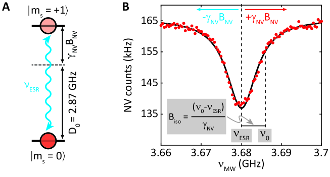
The NV center orbital ground state forms an electronic S=1 spin triplet with magnetic sublevels and a zero field splitting between and of GHzRondin et al. (2014). Figure S1A shows the two level system spanned by the and sublevels, which is used for magnetometry in this work. Upon application of an external magnetic field BNV along the NV-axis, the sublevel experiences a Zeeman shift of
| (1) |
where MHz/mT is the gyromagnetic ratio. As magnetic fields perpendicular to the NV axis have to compete with the zero field splitting , they only yield a second order effect and, can therefore be ignored in this work.
Optical initizalization and read-out of the NV centerGruber et al. (1997) then allows for optical detected magnetic resonance (ODMR) where the NV center is initialized in its bright state and a mircowave driving field at frequency populates the less bright state in the resonance case , leading to a dip in fluoresence (Fig. S1B). The BNV maps shown in the main text have been obtained by recording such ODMR spectra at each pixel of the scan at typical pixel dwell-times of s.
An alternative, faster method to acquire an overview of the magnetic signal originating from a sample is isomagnetic field imaging in which contours of fixed values BBiso are measured. To that end, the microwave frequency is fixed at and the sample is scanned below the NV center while its fluoresence is constantly interrogated. Whenever the sample stray field at the position of the NV corresponds to Biso, a decrease in fluoresence is observed, leading to magnetic contrast in the iso field image. This procedure was used to obtain the data in Fig. 3A of the main text with B.
V Encapsulation of micromechanical cleaved CrI3 crystals
The few-layer CrI3 flakes studied here were micromechanically cleaved from chemical vapour deposition (CVD) grown CrI3 single crystals and then transferred onto nm SiO2/Si wafers inside a N2 filled glovebox (ppm of H2O and ppm of O2). They were then encapsulated using either thin graphite (nm) or hBN (nm) flakes inside the same glove box to avoid degradation in air. Encapsulation was performed via a standard all-dry pick-up and release technique using a polymer stackWang et al. (2013).
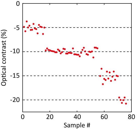
Figure S3A, Fig. S4A and Fig. S5A show optical micrographs of the mono-, bi-, tri-, five- and nine-layers CrI3 crystals whose magnetometry data is discussed in the main text, before encapsulation. Their thickness was determined using the relative optical contrast (red channel) between the CrI3 crystals and the nm SiO2 layerHuang et al. (2017), which was calibrated via the analysis of 80 atomically thin crystals (1 to 4 layers), as shown in Fig. S2. The thickness of the CrI3 was confirmed by atomic force microscope measurements after the encapsulation.
VI Raman spectra of few-layer CrI3 flakes
The Raman scattering experiment was performed using a Horiba scientific (LabRAM HR Evolution) confocal microscope in backscattering geometry. After laser excitation the dispersed light was sent to a Czerni-Turner spectrometer equipped with a groves/mm grating, which resolves the optical spectra with a precision of cm-1. The light was detected with help of a thermopower cooled CCD-array. The excitation wavelength of the laser was nm. The samples were mounted in the cryostat (cryovac KONTI cryostat) with optical access. The Raman peaks were fitted using Lorentzian lineshapes.
VII Sample D1
VIII Sample D2
IX Sample D3
X Magnetic field data
XI Reverse propagation of magnetisation
We deployed a reverse propagation method to retrieve the perpedicular magnetisation Ms(x,y,z=0) of the sample from our measured magnetic field map BNV(x,y,z=z0)Meyer et al. (2004). The method is performed in Fourier space with Fourier-space coordinates in the -plane. The half-space above the sample contains no time-dependent electric fields or currents and therefore
| (2) |
Hence, we can define a magnetic potential such that
| (3) |
where is the gradient in Fourier space.
In order to fulfill Eq.(2), the Laplace equation needs to hold outside the sample, which leads to and . For a purely out-of-plane magnetisation on the sample surface, and, using Eq.(3), we then obtain and therefore
| (4) |
which is the magnetic field generated from the discontinuity of the magnetisation of one surface. In case of a thin film with thickness one also has to consider the magnetic field from the bottom surface. The field in the half-space above the sample then becomes
| (5) |
Introducing the surface moment density and taking the limit of a thin film (), one obtains
| (6) |
Using the above equation for the gradient, the in-plane and perpendicular components of the magnetic field read
| (7) |
| (8) |
The magnetic field along the NV-axis in Fourier space is then given by a single propagator :
| (9) |
In particular by solving Eq.(9) for we can extract the surface magnetisation from the measured data. In this, high-frequency components, and therefore noise, are exponentially enhanced and need to be filtered out. A Hanning windowRoth et al. (1989) low-pass filter is conveniently used to circumvent this problem:
| (10) |
where the cut-off wavelength 2/hNV is here naturally set by the NV sample distance .
Our reverse propagation procedure is then as follows:
-
1.
At each point (x,y) of the scan, the electron spin resonance frequency is fitted and the magnetic field is extracted according to
(11) with MHz being the zero-field splitting of the NV and MHz/mT the electron gyromagnetic ratio.
-
2.
The externally applied bias magnetic field is subtracted from the data set to obtain generated by the sample .
-
3.
Optionally, the magnetic field data is extended outwards and decays towards zero using a Gaussian function. This is especially necessary for all data sets, which do not contain the entire magnetic flakes within the scan range.
-
4.
The magnetic field data is 2D Fourier transformed to obtain . Zero-padding is used to the extent that all resolvable frequencies are well sampled.
-
5.
The magnetic field is transformed to obtain the surface magnetisation using
(12) with an initial guess for , and .
-
6.
The data is transformed to real space and cropped to its original size.
-
7.
The domain boundaries of are found and a homogeneous magnetisation is assumed with . Then, is forward-propagated using the formalism described above, and compared with the original magnetic field data. Using a least square fitting routine, values for , and are found which reproduce the measured magnetic field best.
-
8.
The values for , and determined in step 7. are used to obtain the final moment density profiles using the reverse propagation described by Eq.(12).
XII Non-invasiveness of imaging method
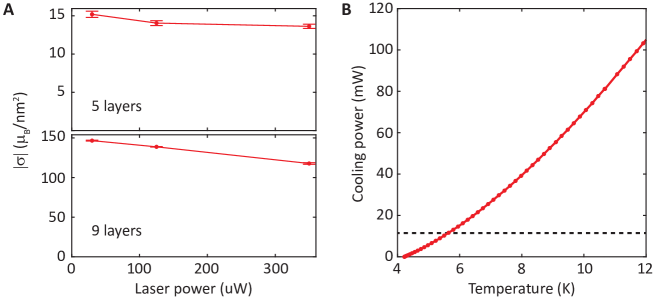
Figure S7: Impact of laser irradiation and microwave heating. Fig. A shows the influence of nm laser power on the magnetisation extracted from linecuts of BNV across the edges of a flake. The top (bottom) panel shows magnetisation of linecuts as indicated in Fig. 2B (Fig. 2C). The linecuts over the 9-layers flake edge were performed after the puncture. Laser powers above W slightly lower the value of measured magnetisation compared to the results obtained at lower powers. Working with W in all data sets ensures that no significant back-action from heating by laser power was induced onto the samples. In B we compare the cooling power of our 4He bath cryostat with the power input of the microwave field required to drive electron spin resonance on the NV center. The estimated microwave power arriving in the cryostat is indicated by the black dashed line. The temperature dependent cooling power of the cryostat is shown with the red dotted line. Heating due to microwave irradiation leads to a measurement temperature of K, which is well below the Curie temperature of monolayer CrI3 (KHuang et al. (2017)).