Weak antilocalization in quasi-two-dimensional electronic states of epitaxial LuSb thin films
Abstract
Observation of large nonsaturating magnetoresistance in rare-earth monopnictides has raised enormous interest in understanding the role of its electronic structure. Here, by a combination of molecular-beam epitaxy, low-temperature transport, angle-resolved photoemission spectroscopy, and hybrid density functional theory we have unveiled the band structure of LuSb, where electron-hole compensation is identified as a mechanism responsible for large magnetoresistance in this topologically trivial compound. In contrast to bulk single crystal analogues, quasi-two-dimensional behavior is observed in our thin films for both electron and holelike carriers, indicative of dimensional confinement of the electronic states. Introduction of defects through growth parameter tuning results in the appearance of quantum interference effects at low temperatures, which has allowed us to identify the dominant inelastic scattering processes and elucidate the role of spin-orbit coupling. Our findings open up possibilities of band structure engineering and control of transport properties in rare-earth monopnictides via epitaxial synthesis.
pacs:
74.20.Rp, 74.25.Jb, 79.60.-iI Introduction
Rare-earth monopnictides are of immense technological and scientific interest due to their potential applications in terahertz sourcesBjarnason:2004jt ; Sukhotin:2003kh ; Salas:2017ia , thermoelectricsLiu:2011hc , solar cellsZide:2006gy , plasmonicsKrivoy:2018el , and as buried epitaxial contactsHanson:2006ir when incorporated in III-V semiconductor heterostructures. Recently, it has been realized that these compounds also exhibit remarkably large magnetoresistance that has been attributed to either electron-hole compensationZeng:2016et ; Han:2017dw ; Yang:2017fj or the presence of topologically nontrivial surface statesFallahTafti:2016kl ; Tafti:2015kj ; Nayak:2016if ; Singha:2017fi . To elucidate the origins of these novel properties and for possible device applications it is thus imperative to gain an understanding of the electronic structure and scattering processes and how they are possibly modified in thin film geometries and/or nanostructures.
Here, we present a demonstration of epitaxial synthesis of LuSb thin films using GaSb buffer layers on GaSb (001) substrates. We have observed Shubnikov de-Haas oscillationsShoenberg from both electron and holelike carriers in our high mobility LuSb thin films, which are found to be in excellent correspondence with angle-resolved photoemission spectroscopy (ARPES) measurements and density functional theory (DFT) calculations with the Heyd-Scuseria-Ernzerhof (HSE06) hybrid functionalHeyd:2003eg ; HSE . This has allowed us to experimentally map out the entire Fermi surface and determine Fermi wave vector (), effective mass (), and carrier concentration () of each of the bands constituting the Fermi surface. Observation of approximately equal concentration of electron and holelike carriers in LuSb coupled with the absence of any topological surface state in our ARPES measurements leads us to identify electron-hole compensation as the likely mechanism for large nonsaturating magnetoresistance observed in this compound. However, in contrast to bulk single crystals, quasi-two-dimensional behavior is observed for all the electronic bands in epitaxial films even with thicknesses as large as 14 nm. This is further corroborated by the observation of two-dimensional weak antilocalization (WAL) effects at low temperatures that also underscores the importance of spin-orbit scattering in this compound. Phase coherence length was found to be limited by electron-phonon scattering down to 2K. However, in comparison to bulk single crystals, Debye temperature () is substantially reduced in our thin films. At low temperatures, characteristic phonon wavelength is found to be larger than the film thickness, placing phonons also in the 2D limit.
II Synthesis and Sample Characterization
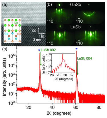
Epitaxial thin films of LuSb (6.055 Å) were synthesized on GaSb (6.095 Å) substrates that are nearly perfectly lattice matched. In addition, the surface atomic arrangement of the antimony (Sb) atoms on the (001) surface provides an excellent template for epitaxial integration of LuSb atomic layers resulting in a continuous Sb sublattice. High angle annular dark field scanning transmission electron microscopy (HAADF-STEM) image shown in Fig. 1(a) confirms excellent quality of our thin films with minimal interdiffusion at the interface. By changing the substrate temperature and/or Lu:Sb beam flux ratio during growth we are able to introduce defects in our thin films that result in the appearance of quantum interference effects at low temperaturessuppl . RHEED images from such thin film samples are shown in Fig. 1(b). Sb-rich c(26) reconstruction is observed for GaSb buffer layers that quickly changes to a (11) reconstruction expected from stoichiometric rock-salt LuSb atomic layers. Out-of-plane - 2 x-ray diffraction (XRD) further confirms that these thin films are single phase with (001) LuSb out-of-plane orientation. Smooth surfaces of our thin films results in thickness fringes from which we estimate a film thickness of 14.2 nm. All transport measurements presented in this work are from samples that exhibited quantum interference effects at low temperatures unless mentioned otherwise.
III Transport properties and electronic structure
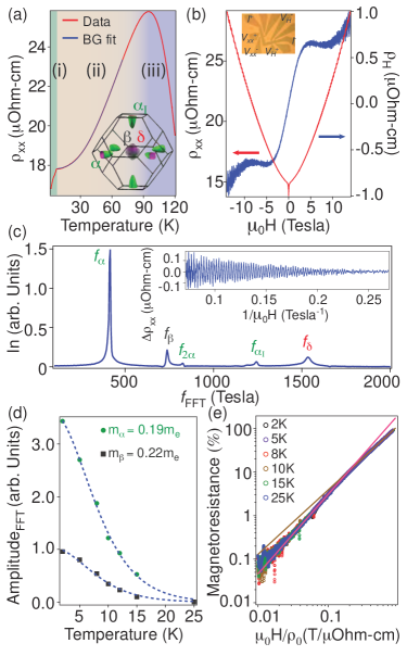
WAL effect becomes manifest in our transport measurements below 8K leading to a dramatic drop in resistivity [Fig. 2(a)] that is readily suppressed on application of magnetic field perpendicular to the sample plane [Fig. 2(b)]. Temperature dependence of resistivity follows Bloch Grüneissen functional formZiman with estimated Debye temperature of = 267 K, which is much smaller in magnitude compared to what has been found in single crystalsPavlosiuk:2017fh , and in other Lu monopnictidesogaA:2014km . Transverse magnetoresistance shows nonsaturating behavior and reaches 110 at 14 T field. Magnetoresistance curves taken at different temperatures follow Kohler’s scalingZiman = , shown in Fig. 2(e), indicating single dominant scattering process. However, unlike in single crystals the value of the exponent changes from 1.835 in the low field, high temperature regime to 1.486 in the high field, low temperature regime. Hall resistance shows multicarrier behavior as is expected from a compensated semimetal such as LuSb. Longitudinal and Hall resistivities were used to estimate mobility () and diffusion coefficient (D) of each of the electronic bands (see Table I and Ref. suppl ).
| 111FS denotes Fermi surface, nSdH and nDFT are the carrier concentrations obtained from SdH and DFT, respectively, vF is the Fermi velocity, is the mobility, D is the diffusion constant, is the elastic scattering length, and is the corresponding characteristic magnetic field. vF, , D, , and are calculated from data taken at 8 K suppl . Average value of is calculated as , where the average is taken over all of the electronic bands in LuSb.FS | nSdH(cm-3) | nDFT(cm-3) | vF(m/s) | (cm2/Vs) | D(m2/s) | (nm) | (T) |
| 1.4351020 | 1.451020 | 1.01106 | 5.42102 | 0.06 | 59 | 0.047 | |
| 1.151020 | 1.171020 | 7.893105 | 4.078103 | 0.318 | 403 | 0.001 | |
| 3.431020 | 2.921020 | 6.367105 | 2.036103 | 0.188 | 295 | 0.002 |
We observe clear evidence of Shubnikov de-Haas (SdH) oscillations for fields stronger than 3.5 T, which is extracted after subtracting a smooth fifth order polynomial from the magnetoresistance data, shown in the inset of Fig. 2(b). Characteristic frequencies corresponding to an electron pocket at the zone edge (, ) and two hole pockets at the zone center (, ) are identified that match very well with both ARPES measurements and predictions from DFT calculations, summarized in Table II. Our results indicate that LuSb is a compensated semimetal with = 1.06. From thermal damping of the amplitude of SdH oscillationsShoenberg , where , we estimate the effective masses for the and pocket to be 0.19me and 0.22me, respectively.
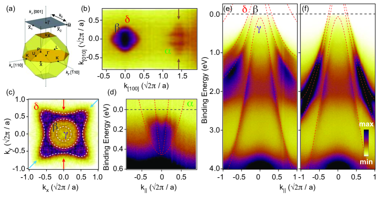
In Fig. 3, we present E - k spectral map along both and directions of the surface Brillouin zone for the hole pockets and along for the electron pocket. Effective masses are determined from parabolic fittings of the band dispersions at the Fermi levelsuppl , which are in agreement with SdH and DFT results. Surface projection of the elliptical electron pocket allowed us to estimate effective masses along both the semimajor and semiminor axes of the ellipse (see Table II). We observe three holelike bands near the point with the third band () completely below the chemical potential in agreement with our DFT calculations. We must highlight the importance of using hybrid functionalsHeyd:2003eg in DFT calculations of rare-earth monopnictides. Use of generalized gradient approximation (GGA)Perdew:1996iq erroneously predicts that all three holelike bands in LuSb cross the Fermi level, in clear disagreement with both our ARPES and quantum oscillation resultssuppl .
| kF (Å-1) | m∗ | |||||
|---|---|---|---|---|---|---|
| FS222FS denotes Fermi Surface | SdH | ARPES | DFT | SdH | ARPES | DFT |
| 0.11(), 0.34()333 and indicates directions along the semiminor and semimajor axes of the elliptical pocket, respectively. | 0.1(), 0.38() | 0.11(), 0.37() | 0.19 | 0.09(), 1.02() | 0.11(), 1.16() | |
| 0.15 | 0.12(1), 0.12()4441 and indicates [100] and [110] crystallographic directions, respectively. | 0.15(1), 0.15() | 0.22 | 0.26(1), 0.26() | 0.23(1), 0.21() | |
| 0.22 | 0.21(1), 0.19() | 0.24(1), 0.19() | — | 0.45(1), 0.36() | 0.54(1), 0.31() | |
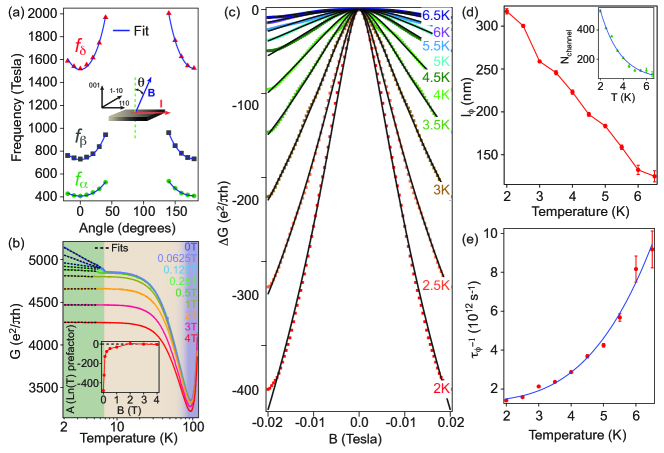
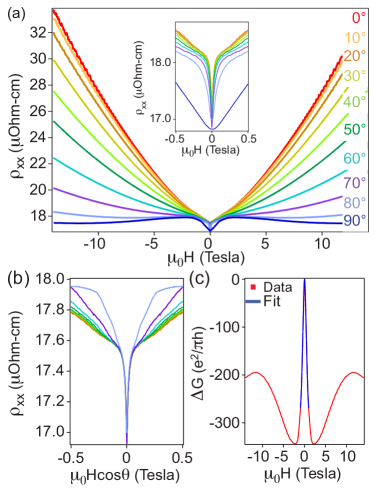
Having established the fermiology of our LuSb thin films we now turn to the magnetotransport results. Angle-dependent magnetotransport shows quasi-two-dimensional behavior for all the electronic bands in LuSb in marked contrast to its bulk single crystal analoguesPavlosiuk:2017fh . The angular dependence of the SdH frequencies follows a 2D Fermi surface model , where is the angle between the magnetic field vector and normal to the sample plane and is the SdH frequency at = 0. Although a similar angle-dependent behavior is expected from the bulk elliptical bandHan:2017dw , an ellipticity ( / ) much greater than the measured value of 3 is required to satisfactorily fit the observed angular dependence. Observed onset fields at which SdH oscillations begin to appear for different angular orientation further lends support to its quasi-2D behaviorsuppl ; Allen:1991ut .
IV Analysis of quantum interference effects
Thin films can be treated as quasi-two-dimensional if the film thickness is smaller than the relevant length scales. Electronic mean free paths ( ) for all the electronic bands are found to be greater than the film thickness (see Table I), placing classical diffusive transport in our films in the 2D limit. WAL effects appearing in our thin films can also be considered as two dimensional as the associated characteristic length scale is the phase coherence length (), which is required to be much greater than for such effects to appear in the first place and hence, must also be greater than the thickness of our thin film.
Presence of quantum interference effects, such as WAL in two dimensions, leads to an additional contribution to low temperature electron conductance )Hikami:wh , being the characteristic temperature. The prefactor A is negative for strong spin-orbit scattering ( , and are the spin-orbit and dephasing time, respectively)(WAL), in agreement with our experimental observation, shown in Fig. 4(b). Next, we utilize temperature dependence of the quantum interference effects under a perpendicular magnetic field to estimate phase coherence lengths using Hikami-Larkin-Nagaoka (HLN) theory Hikami:wh for two-dimensional electron gas in the diffusive limit that assumes Elliot-Yafet (E-Y)Lee:1985 ; AA:1983 ; Elliott:1954fv ; Yafet:1963 spin-orbit scattering mechanism. The centrosymmetric rock-salt crystal structure of LuSb coupled with the lack of evidence of Rashba-split states in our ARPES data guarantees that both the Dresselhaus and the Rashba effectsWinkler are unimportant in LuSb precluding us from considering Dyakonov-Perel (D-P)Dynakov:1972 scattering mechanism as a likely origin for the observed WAL effects.
At low magnetic fields under strong spin-orbit coupling HLN theory predicts quantum correction to conductance under perpendicular magnetic field asHikami:wh
| (1) |
where is the number of parallel 2D channels, is the digamma function, is the characteristic magnetic field corresponding to the phase coherence length , and in the limit of strong spin-orbit scattering.
We note that the magnitude of the quantum correction effects in our thin films is relatively large, which would generally be construed as arising from three-dimensional carriers. However, evidence provided so far leads us to consider the electronic states as quasi-two-dimensional indicating the presence of a large number of quasi-2D channels in our thin films due to dimensional confinement. Good fits to the WAL data are achieved using HLN theory, as shown in Fig. 4(c). Phase coherence lengths, shown in Fig. 4(d) are found to be much larger than the film thickness, thus validating our initial assumption of the applicability of the HLN theory for a two-dimensional electron gas. We find a T-n dependence of the dephasing time () with down to the lowest measured temperature of 2K that can be ascribed to electron-phonon scattering in a two-dimensional electronic systemLin:2002dt . We estimate phonon velocity = 1.69 km/s and the characteristic phonon wavelength 40.5nm at 2Ksuppl , which is greater than the film thickness. Therefore, at the lowest measured temperatures phonons in our thin films should be considered as quasi-two-dimensional. The number of independent two-dimensional channels () estimated from the fits decreases exponentially with increasing temperature plausibly due to enhanced inter subband scattering at higher temperatures.
The quantum corrections appearing at low temperatures in our magnetotransport data are found to be sensitive to the normal component of the magnetic field vector, as shown in Figs. 5(a) and (b), further underscoring the quasi-2D nature of the electronic states in our thin films. We provide one final piece of evidence for the quasi-two-dimensional nature by examining WAL effects that appear when the magnetic field vector is in the film plane. For an ideal 2D system no WAL induced magnetoresistance is expected in this measurement configuration. However, nonzero electron diffusion in the out-of-plane film direction always results in a finite WAL effect on application of in-plane magnetic field. 2D WAL corrections in such a configuration in the strong spin-orbit regime are given byAA:1981 ; DK:1984 ; Beenakker:1988tf
| (2) |
where = ( is the film thickness) and is equal to 13.2 T in our case, = + , = . is the characteristic magnetic field corresponding to the spin-orbit scattering length . We have ignored spin-flip scattering in our LuSb thin films, which is nonmagnetic. The above equation is valid for magnetic field strengths less than 1.65 T beyond which the characteristic magnetic length, given by , exceeds the film thickness and transport in our thin films can no longer be considered two dimensional. Our data under parallel magnetic field is described very well by the 2D theory, as shown by the fit in Fig. 5(c), with the same and values as obtained from perpendicular field magnetoresistance, with BSO and as the free parameters. We obtained a spin orbit scattering length of 90.7 nm at 2K, which is much smaller than the phase coherence length of 317.4 nm and a value of 0.097. is expected to be equal to , when AA:1981 and is () in the opposite limitDK:1984 . Estimated elastic scattering length () in our thin film is greater than that of the film thickness (), which should place us in the Dugaev-Khimel’nitskii limitDK:1984 . However, our estimated value suggests an intermediate regime scenarioBeenakker:1988tf , where () , which is attributed to additional contribution from inter subband scattering due to the presence of multiple parallel 2D channels in our thin films. Magnetoconductance in our thin films becomes positive at intermediate field values beyond 2.3 T, reminiscent of the observed parallel field magnetoconductance for 2D channels in III-V semiconductors, suggestive of reduced inter sub-band scattering at higher fieldsEnglert:1983 . It becomes negative again at a stronger field of 11.4 T when the thin film is firmly in the 3D limit plausibly due to dominant contribution of classical magnetoresistance at high field values.
V Methods
V.0.1 Thin film growth
Thin films were grown by molecular-beam epitaxy (MBE) in a MOD Gen II growth chamber. A 5-nm-thick GaSb buffer layer was grown on low n-type doped GaSb (001) substrates (that freezes out at low temperatures, see Ref. suppl ) at 450∘C under Sb4 overpressure after desorption of the native oxide using atomic hydrogen. This is followed by co-evaporation of Lu and Sb from calibrated effusion cells with the substrate temperature at 285∘C - 380∘C and Lu to Sb flux ratio ranging between 1:1 and 1:4. Samples grown at lower Lu:Sb flux ratio and/or lower substrate temperature resulted in films that did not show weak antilocalization effects. Atomic fluxes of Lu and Sb are calibrated by Rutherford backscattering spectrometry (RBS) measurements of the elemental areal density of calibration samples on Si. These measurements were used to calibrate in situ beam flux measurements using an ion gauge. Sample surfaces were protected with a 10-nm-thick AlOx layer using e-beam evaporation before taking them out of the UHV chamber. For ARPES measurements conductive n-type Te doped GaSb (001) substrates were used.
V.0.2 Low-temperature transport
Transport measurements were performed on a fabricated hall-bar device using standard a.c. lock-in technique at low temperatures with the current flowing along [110] crystallographic direction where parallel conduction from the substrate and the buffer layers can be neglected [see Fig. 2(a) and Ref. suppl ). Hall bars were fabricated using standard optical lithography, followed by an ion milling procedure using argon ions. Contacts were made using 50 m gold wire bonded onto gold pads. Low temperature measurements were carried out in a Quantum Design PPMS with base temperature of 2K and maximum magnetic field of 14T.
V.0.3 ARPES
Samples were transferred in a custom-built vacuum suitcase from the growth chamber at Santa Barbara to the ARPES endstation 10.0.1.2 at the Advanced Light Source in Berkeley. Pressure inside the vacuum suitcase was better than 110-10 Torr. Tunable synchrotron light in the 20-80 eV range was used for photoemission measurement with a Scienta R4000 analyzer. The base pressure of the analysis chamber was better than 510-11 Torr.
V.0.4 HAADF-STEM
High-angle annular dark field scanning transmission electron microscopy (HAADF-STEM) was used for imaging the cross section of the epitaxial layer. The cross-sectional lamellas for STEM were prepared using a FEI Helios Dual-beam Nanolab 650 focused gallium ion beam (FIB). FIB etching steps down to 2KeV were used to polish down the lamella to approximately 50 nm in thickness.
V.0.5 Computational approach
The calculations were based on density functional theory (DFT)hohenberg1964inhomogeneous ; kohn1965self and the hybrid functional of Heyd, Scuseria, and Ernzerhof (HSE06)Heyd:2003eg ; HSE as implemented in the VASP codekresse1993ab ; kresse1994ab . The interaction between the valence electrons and the ionic cores was described using projector augmented-wave (PAW) potentials blochl1994projector ; kresse1999ultrasoft . The PAW potential for Sb has five valence electrons with 5s25p3 configuration, whereas for Lu there are nine valence electrons, i.e., 5p66s25d1 configuration. Test calculations including the localized Lu 4 orbitals in the valence showed a dispersionless fully occupied 4 bands at eV below the Fermi level, and change the calculated carrier density by less than 5%. We used a plane-wave basis set with 300 eV kinetic energy cutoff and 8x8x8 -centered mesh of k points for integrations over the Brillouin zone of the primitive cell of rock-salt crystal structure with two atoms, one located at (0,0,0) and the other at (0.5,0.5,0.5). SuperCell K-space Extremal Area Finder (SKEAF)Julian2012 and Wannier90Mostofi2014 codes were used for the calculation of carrier density and SdH frequencies, whereas the effective mass was calculated at the Fermi level by getting the second derivative.
VI Conclusion
In summary, we have demonstrated our ability to synthesize high quality LuSb thin films and controllably introduce defects to access diffusive regime in transport measurements. By employing quantum oscillations, ARPES, and DFT calculations we have thoroughly characterized its electronic structure that establishes LuSb as a compensated semimetal and topologically trivial. Large phase coherence lengths coupled with strong spin-orbit scattering led to the observation of weak antilocalization at low temperatures. Quasi-two-dimensionality of the electronic states, significant reduction of the Debye temperature from its bulk value, and accessibility to the two-dimensional limit of the phonon spectrum offers opportunities to control electron-phonon coupling in epitaxial thin films. Furthermore, recent DFT calculations predict the possibility of a topological phase transition in LuSb and LuBi on application of bi-axial strainNarimani:2018bc , which should now be accessible to experimentalists. Our work lays the foundation for further studies of controlled tunability of the electronic properties via epitaxial strain, dimensional confinement and electrostatic gating in this technologically relevant material system for novel device applications.
Acknowledgements
The authors thank S. James Allen for helpful discussions. Synthesis of thin films, development of the UHV suitcase, ARPES experiments, and theoretical work are supported by the US Department of Energy (Contract No. DE-SC0014388). Development of the growth facilities and low temperature magnetotransport measurements are supported by the Office of Naval Research through the Vannevar Bush Faculty Fellowship under the Award No. N00014-15-1-2845. This research used resources of the Advanced Light Source, which is a DOE Office of Science User Facility under contract no. DE-AC02-05CH11231. We acknowledge the use of facilities within the National Science Foundation Materials Research and Engineering Center (DMR 11-21053) at the University of California at Santa Barbara, the LeRoy Eyring Center for Solid State Science at Arizona State University. Density functional theory calculations made use of the Extreme Science and Engineering Discovery Environment, NSF Grant No. ACI-1053575, and high-performance computing and the Information Technologies resources at the University of Delaware. D.R. gratefully acknowledges support from the Leverhulme Trust via an International Academic Fellowship (IAF-2018-039).
References
- (1) J. E. Bjarnason, T. L. J. Chan, A. W. M. Lee, E. R. Brown, D. C. Driscoll, M. Hanson, A. C. Gossard, R. E. Muller Appl. Phys. Lett. 85 (18), 3983–3985 (2004).
- (2) M. Sukhotin, E. R. Brown, A. C. Gossard, D. Driscoll, M. Hanson, P. Maker, R. Muller Appl. Phys. Lett. 82 (18), 3116–3118 (2003).
- (3) R. Salas, S. Guchhait, S. D. Sifferman, K. M. McNicholas, V. D. Dasika, D. Jung, E. M. Krivoy, M. L. Lee, S. R. Bank, APL Mater. 5 (9), 096106–096108 (2017).
- (4) X. Liu, A. T. Ramu, J. E. Bowers, C. J. Palmstrøm, P. G. Burke, H. Lu, A. C. Gossard, J. Cryst Growth 316 (1), 56–59 (2011).
- (5) J. M. O. Zide, A. Kleiman-Shwarsctein, N. C. Strandwitz, J. D. Zimmerman, T. Steenblock-Smith, A. C. Gossard, A. Forman, A. Ivanovskaya, G. D. Stucky, Appl. Phys. Lett. 88 (16), 162103–162104 (2006).
- (6) E. M. Krivoy, A. P. Vasudev, S. Rahimi, R. A. Synowicki, K. M. McNicholas, D. J. Ironside, R. Salas, G. Kelp, D. Jung, H. P. Nair, G. Shvets, D. Akinwande, M. L. Lee, M. L. Brongersma, S. R. Bank, ACS Photonics 5 (8), 3051–3056 (2018).
- (7) M. P. Hanson, A. C. Gossard, E. R. Brown, Appl. Phys. Lett. 89 (11), 111908–4 (2006).
- (8) L.-K. Zeng, R. Lou, D.-S. Wu, Q. N. Xu, P.-J. Guo, L.-Y. Kong, Y.-G. Zhong, J.-Z. Ma, B.-B. Fu, P. Richard, P. Wang, G. T. Liu, L. Lu, Y.-B. Huang, C. Fang, S.-S. Sun, Q. Wang, L. Wang, Y.-G. Shi, H. M. Weng, H.-C. Lei, K. Liu, S.-C. Wang, T. Qian, J.-L. Luo, H. Ding, Phys. Rev. Lett. 117, 127204 (2016).
- (9) F. Han, J. Xu, A. S. Botana, Z. L. Xiao, Y. L. Wang, W. G. Yang, D. Y. Chung, M. G. Kanatzidis, M. R. Norman, G. W. Crabtree, W. K. Kwok, Phys. Rev. B 96 (12), 125112 (2017).
- (10) H. Y. Yang, T. Nummy, H. Li, S. Jaszewski, M. Abramchuk, D. S. Dessau, F. Tafti, Phys. Rev. B 96 (23), 235128 (2017).
- (11) F. F. Tafti, Q. Gibson, S. Kushwaha, J. W. Krizan, N. Haldolaarachchige, R. J. Cava, Proc. Natl. Acad. Sci. U.S.A. 113 (25), E3475–E3481 (2016).
- (12) F. F. Tafti, Q. D. Gibson, S. K. Kushwaha, N. Haldolaarachchige, R. J. Cava, Nature Phys. 12 (3), 272–277 (2015).
- (13) J. Nayak, S.-C. Wu, N. Kumar, C. Shekhar, S. Singh, J. Fink, E. E. D. Rienks, G. H. Fecher, S. S. P. Parkin, B. Yan, C. Felser, Nat. Commun, 8, 13942 (2017).
- (14) R. Singha, B. Satpati, P. Mandal, Sci. Rep.7, 6321 (2017).
- (15) D. Shoenberg, Magnetic Oscillations in Metals (Cambridge University Press, Cambridge, 1984).
- (16) J. Heyd, G. E. Scuseria, M. Ernzerhof, J Chem. Phys. 118 (18), 8207–8215 (2003).
- (17) J. Heyd, G. E. Scuseria, M. Ernzerhof, J. Chem. Phys 124, 219906 (2006)
- (18) See Supplemental Material at https://link.aps.org/supplemental/DOI for a) Dependence of transport properties on growth conditions b) Estimation of transport parameters c) Estimation of phonon wavelength d) Critical magnetic field value for Shubnikov-deHaas oscillations in tilted fields e) Parabolic fits to the ARPES data f) Evolution of the FFT frequencies in LuSb thin films under tilted fields g) Comparison between resistances of GaSb and LuSb and h) Comparison between the DFT results obtained utilizing GGA and HSE hybrid functionals.
- (19) Z. M. Ziman, Electrons and Phonons, Clarendon Press, Oxford (1960).
- (20) O. Pavlosiuk, M. Kleinert, P. Swatek, D. Kaczorowski, P. Wisniewski, Sci. Rep. 7, 12822 (2017)
- (21) O. Zogal, R. Wawryk, M. Matusiak, Z. Henkie, J. Alloys Compd. 587 (C), 190–198 (2014).
- (22) J. Perdew, K. Burke, M. Ernzerhof, Phys. Rev. Lett. 77 (18), 3865 (1996).
- (23) S. J. Allen, F. DeRosa, C. J. Palmstrøm, A. Zrenner, Phys. Rev. B 43 (12), 9599 (1991).
- (24) S. Hikami, A. I. Larkin, Y. Nagaoka, Prog. Theor. Phys. 63, 707 (1980).
- (25) P. M. Lee, T. V. Ramakrishnan, Rev. Mod. Phys. 57, 287 (1985).
- (26) B. L. Al’tshuler, A. G. Aronov, Solid State Commun. 46, 429 (1983).
- (27) R. J. Elliott, Physical Review 96 (2), 266 (1954).
- (28) Y. Yafet, Sol. St. Phys. 14, 1–98 (1963).
- (29) R. Winkler, Spin-orbit coupling effects in two-dimensional electron and hole systems (Springer, Berlin, 2003)
- (30) M. I. Dyakonov, V. I. Perel, Sov. Phys. Sol. St., USSR, 13, 3023 (1972).
- (31) J. J. Lin, J. P. Bird, J. Phys. Condens. Matter 14, R501 (2002).
- (32) B. L. Al’tshuler, A. G. Aronov, JETP Lett. 33, 499 (1981).
- (33) V. K. Dugaev, D. E. Khimel’nitskii, JETP Lett. 59, 1038 (1984).
- (34) C. Beenakker, H. van Houten, Phys. Rev. B 38 (5), 3232 (1988).
- (35) Th. Englert, J. C. Maan, D. C. Tsui, A. C. Gossard, Solid State Commun. 45, 989 (1983)
- (36) M. Narimani, S. Yalameha, Z. Nourbakhsh, J Alloys Compd 768, 1–8 (2018).
- (37) P. Hohenberg, W. Kohn, Phys. Rev. 136, (B864), (1964)
- (38) W. Kohn, L. J. Sham, Phys. Rev. 140, A1133 (1965)
- (39) G. Kresse, J. Hafner, Phys. Rev. B 47, 558 (1993)
- (40) G. Kresse, J. Hafner, Phys. Rev. B 49, 14251 (1994)
- (41) P. E. Blöchl, Phys. Rev. B 50, 17953 (1994)
- (42) G. Kresse, D. Joubert, Phys. Rev. B 59, 1758 (1999)
- (43) S. R. Julian, Comput. Phys. Commun.183, 324 (2012)
- (44) A. A. Mostofi, J. R. Yates, G. Pizzi, Y. S. Lee, I. Souza, D. Vanderbilt, N. Mazari, Comput. Phys. Commun. 185, 2309 (2014)