Enhanced electron-phonon interaction in multi-valley materials
Abstract
We report a new mechanism responsible for the enhancement of electron-phonon coupling in doped semiconductors in which multiple inequivalent valleys are simultaneously populated. We have identified this mechanism through a combined experimental and theoretical investigation of the vibrational properties of atomically thin group-VI semiconducting transition metal dichalcogenides as a function of carrier density. Specifically, we have performed Raman spectroscopy experiments to measure different phonon modes of mono and bilayer MoS2, WS2, and WSe2 embedded in ionic-liquid-gated field-effect transistors, and probed vibrations of these systems over a wide range of carrier densities ( cm-2, both for electron and hole accumulation). We find that in-plane modes, such as the E2g mode, are insensitive to the introduction of charge carriers, whereas phonons with a dominant out-of-plane character exhibit strong softening upon electron accumulation, while remaining unaffected upon hole doping. This unexpected –but very pronounced– electron-hole asymmetry is systematically observed in all mono and bilayers. To understand its origin, we have performed first-principles simulations within a framework that accounts for the reduced dimensionality of the systems and gate-induced charge accumulation. Through this analysis we establish that the phonon softening occurs when multiple inequivalent valleys are populated simultaneously and that the phenomenon is a manifestation of an aspect of electron-phonon interaction that had not been previously identified. Accordingly, the observed electron-hole asymmetry in the evolution of the Raman spectra originates from the the much larger energy separation between valleys in the valence bands –as compared to the conduction band– that prevents the population of multiple valleys upon hole accumulation. We discuss the origin of the enhancement of the electron-phonon coupling in terms of a simple physical picture, and conclude that the phenomenon occurs because the population of multiple valleys acts to strongly reduce the efficiency of electrostatic screening for those phonon modes that cause the energy of the inequivalent valleys to oscillate out of phase. The strong enhancement of electron-phonon coupling in the presence of multivalley populations is a robust mechanism that is likely to play an important role in accounting for different physical phenomena and, based on existing experiments, we argue for its relevance in the occurrence of superconductivity –either gate-induced or spontaneous– in different transition metal dichalcogenides.
I Introduction
The electronic and elastic properties of solids are determined by the interaction between charge carriers and the elementary excitations associated with the vibration of the crystalline lattice, namely the phonons. In view of its fundamental relevance, the nature of the interaction between electrons and phonons has been investigated in great depth in many different contexts Ziman ; Grimvall ; Mahan . In the simplest possible terms, electron-phonon interaction can be understood as originating from the electrostatic potential generated by the lattice distortion associated to the ionic displacement in the presence of a phonon. In other words, exciting a phonon in a crystal displaces the charged ions forming the lattice from their equilibrium positions, thereby generating a local charge imbalance and a corresponding electrostatic potential (known as deformation potential Bardeen1950 ; Schockley1950 ), which in turns directly acts on all mobile electrons.
Depending on the specific type of material considered and on the level of detail needed for a precise microscopic understanding, the situation can be more complex. For instance, in some systems (among which, graphene) the coupling between the lattice deformation associated to certain phonon modes and charge carriers is more appropriately described in terms of a vector potential, rather than an electrostatic one Pietronero1980 ; Sohier2014 . In these cases, charge carriers interact with phonons more similarly to the way they interact with a magnetic field Vozmediano2010 . Also, the influence of electron-phonon interaction on physical phenomena depends strongly on whether the energy and momentum relaxation of electrons is fast or slow relative to the phonon frequency, corresponding to the so-called adiabatic or anti-adiabatic limit of electron-phonon coupling Engelsberg1963 ; Maksimov1996 .
Irrespective of the specific situation, what is key to understand electron-phonon interaction (and its strength) in solids is electrostatic screening Mahan . Indeed, the deformation potential generated by the excitation of a long wavelength phonon tends to be screened by the spatial redistribution of the electrons present in the system, which self-consistently reduce the strength of the electron-phonon coupling Bogulsawski1977 ; Khan1984 ; Kartheuser1986 . Screening is expected to be much more effective in the adiabatic regime –since then electrons are able to equilibrate sufficiently fast in response to the ionic motion– and a much weaker electron-phonon coupling is accordingly expected in this regime as compared to the antiadiabatic one. Conversely, if the nature of the electron-phonon coupling is properly described in terms of a vector potential, as we mentioned it is the case for some of the phonons in graphene ferrari_raman_2007 ; ferrari_raman_2013 , screening cannot influence electron-phonon coupling Sohier2014 ; Pisana2007 (just simply because no spatial distribution of charge carriers can screen a magnetic field). In this case, electron-phonon coupling is expected not to be significantly affected by the presence of charge carriers.
In semiconducting materials hosting only a small density of mobile charges, electrostatic screening is poor and a strong electron-phonon interaction is expected. Addition of charge carriers (e.g., by doping) can drastically improve screening and cause the strength of electron-phonon interaction to decrease, as observed in a variety of semiconductors (e.g., SrTiO3 kirzhnits_description_1973 ; van_mechelen_electron-phonon_2008 ; Wang2016 and other transition metal oxides Verdi2017 ). For those cases in which phonons are not effectively screened by the presence of mobile charges (see example above), it can also happen that addition of charge carriers leaves the strength of electron-phonon interaction unaffected Sohier2014 . In virtually no case, however, the strength of electron-phonon interaction in a semiconductor is expected to increase significantly upon adding charge carriers.
In contrast with this established understanding, here we uncover a yet unidentified mechanism that causes a very significant strengthening –and not a weakening– of electron-phonon coupling in atomically-thin semiconductors upon increasing electron density. Our work relies on a joint experimental and theoretical investigation of Raman spectroscopy performed on mono and bilayers of different semiconducting transition metal dichalcogenides (TMDs; MoS2, WS2, and WSe2) as a function of density of accumulated charge carriers. By integrating all these atomically-thin layers in ionic-liquid-gated field-effect transistors (FETs) we have measured the evolution of the Raman spectrum as a function of electron and hole density up to approximately 51013 cm-2. In all investigated mono and bilayers, the experiments reveal unambiguously that the electron-phonon interaction systematically softens out-of-plane vibrational modes only when electrons are accumulated in the FET channel, while leaving them unaffected upon hole doping. To identify the origin of this unexpected electron-hole asymmetry we have performed density-functional-theory (DFT) calculations in the most realistic framework currently available, accounting for the reduced dimensionality of the materials and for the presence of a finite density of charge carriers Sohier2017 . The calculations allow us to conclude that the observed phonon softening originates from a pronounced increase in the strength of the electron-phonon coupling that occurs whenever the charge carriers in the systems populate simultaneously two inequivalent valleys. Besides accounting for the observed electron-hole asymmetry (as a direct consequence of the different valley structure in the conduction and valence bands of atomically-thin semiconducting TMDs), this finding reveals an aspect of electron-phonon coupling that had not yet been appreciated. Specifically, the strengthening of the electron-phonon coupling is caused by charge transfer between the inequivalent valleys induced by the deformation potential associated to out-of-plane vibrational modes: being local in real space, this inter-valley charge transfer decreases the density of charge that can be displaced, thereby suppressing the effectiveness of electrostatic screening. The phenomenon –expected to be of rather general validity– had not been identified so far, most likely because the models commonly used to describe electron-phonon interaction theoretically do not consider the presence of multiple inequivalent valleys. Equipped with the understanding resulting from the work presented here, we discuss how existing experiments on superconductivity in TMDs (both gate-induced ye_superconducting_2012 ; jo_electrostatically_2015 ; lu_full_2018 and spontaneously occurring Hamaue1986 ; Guillamon2008 ; Xi2016 ; Ugeda2016 ; Tsen2016 ) provide evidence correlating the enhancement in electron-phonon interaction due to multivalley populations to the occurrence of the superconducting state.
II Experimental results
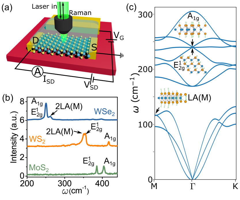
Our experiments consist in measurements of the Raman spectrum of mono and bilayers of different semiconducting TMDs (WSe2, WS2, and MoS2) as a function of carrier density. The density and polarity of charge carriers is varied continuously by employing these atomically-thin crystals as active parts of ionic liquid gated field-effect transistors (see Fig. 1(a) for a schematic illustration). It has been shown in a multitude of experiments over the last several years that ionic-liquid gating is extremely effective in combination with semiconducting TMDs, as it allows the accumulation of large densities (even in excess of 1014 cm-2) of both electrons and holes in a same device braga_quantitative_2012 ; ye_superconducting_2012 ; zhang_electrically_2014 ; lezama_surface_2014 ; jo_mono-_2014 ; ubrig_scanning_2014 ; ponomarev_ambipolar_2015 ; jo_electrostatically_2015 ; zhang_ambipolar_2012 ; costanzo_gate-induced_2016 ; gutierrez-lezama_electroluminescence_2016 . One of the characteristic manifestations of the possibility to vary the charge density and type over such a large interval is the occurrence of ambipolar transport, which can be observed upon sweeping the gate voltage VG (see Fig. 2(a) for an example). In the present context, the occurrence of ambipolar transport is useful because it allows us to obtain a fairly accurate estimate of the carrier density in the devices used for the Raman measurements in-situ. In practice, in the experiments we record the Raman spectrum at many different values of applied gate voltage and –as we vary VG– we also apply a small bias voltage, VSD between the source and the drain electrode to measure the current, ISD, passing through the transistor channel. This allows us to determine the threshold voltage for electron and hole conduction – and – from which we directly estimate the density of electrons and holes at any given value of VG as and (where is the capacitance per unit area obtained from previous experiments on analogous devices, in which Hall effect measurements were performed to determine the density of charge carriers). We estimate the uncertainty in the value of carrier density extracted in this way to be approximately 20-30 %, which is sufficient for the purpose of this work (a more precise determination would require measuring the Hall resistance using a superconducting magnet which cannot be done in the same set-up that we use to perform Raman spectroscopy). For more details concerning the fabrication and operation of ionic-liquid FETs based on atomically-thin TMDs we refer the reader to our earlier work (Refs. braga_quantitative_2012, ; jo_mono-_2014, ; ponomarev_ambipolar_2015, ) and to Appendix A.
Characteristic Raman spectra from bare monolayers of WSe2 (blue line), WS2 (orange line), and MoS2 (green line) are shown in Fig. 1(b). We focus on the most prominent features in these spectra, whose assignment in terms of Raman active vibrational modes has been discussed extensively in the literature lee_anomalous_2010 ; Molina-Sanchez2011 ; berkdemir_identification_2013 ; sahin_anomalous_2013 ; saito_raman_2016 . Using for simplicity the same nomenclature as in the bulk, these are the in-plane (E2g) and the out-of-plane (A1g) modes, as indicated in Fig. 1(b), which are seen in all group VI TMDs. For WS2 and MoS2 these features are spectrally separated while for WSe2 the modes hybridize due to an accidental degeneracy in the phonon dispersion relation, and appear as a single peak at about 250 cm-1. The degeneracy is also present in the calculated phonon dispersion relation of WSe2 in Fig. 1(b), on which we point to the modes observed in the Raman spectroscopy data. For most peaks the observed frequency corresponds to the value of the corresponding mode at the -point. However one of the peaks, visible in the spectra of both WSe2 and WS2 and labeled 2LA(M) (see Fig. 1(b)), is due to a double resonant process terrones_new_2014 ; mitioglu_second-order_2014 , which occurs because the frequency of the laser used in our measurements matches an electronic transition (C absorption for WSe2 and the B-exciton for WS2) carvalho_band_2013 . Although it is not the main point of interest here, the possibility to observe this mode is relevant because it allows the investigation of the coupling between electrons and phonons at finite momentum, i.e. away from center of the Brillouin zone, as indicated by the corresponding label LA(M) in Fig. 1(c).
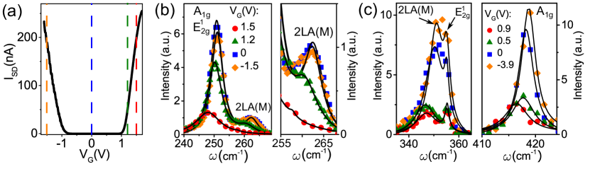
To illustrate the results of our Raman spectroscopy measurements as a function of accumulated charge density we start by discussing the case of WSe2 monolayers. The source-drain current ISD as a function of VG (for VSD = 50 mV) measured in the device used for the Raman measurements, is presented in Fig. 2(a) and exhibits clear ambipolar behavior. The increase of ISD at positive values of VG indicates accumulation of electrons in the FET channel while the increase of ISD at negative VG corresponds to the accumulation of holes. As explained above, we use these measurements to estimate the density of electrons and holes as a function of VG. Fig. 2(b) shows the Raman spectra measured for selected values of VG indicated by the vertical dashed lines in Fig. 2(a). For positive values of VG electrons are accumulated (green and red lines, i.e. VG = +1.2 and +1.5 V, corresponding respectively to and cm-2), for negative VG values the gate accumulates holes (orange line, i.e. VG = -1.5 V, corresponding to cm-2), whereas for VG = 0 V (blue line) the chemical potential is in the gap and the semiconductor is neutral capa . Upon electron accumulation the Raman peak originating from the hybridized A1g/E2g mode exhibits a clear softening, shifting towards lower wavenumbers by an amount cm-1, as well as a decrease in intensity as compared to VG = 0 V case. In contrast, accumulation of holes leaves the Raman spectrum virtually unchanged: the peak does not exhibit any appreciable shift, and only its height decreases slightly. The same trends upon varying VG are observed for the resonant Raman peak originating from the 2LA(M) mode, shown in the right panel of Fig. 2(b) 2LAm .
Since in WSe2 monolayers the degeneracy of the E2g and A1g modes prevents us to study separately the evolution of the two individual Raman peaks upon accumulation of charge carriers, in Fig. 2(c) we show data from bilayer WS2, in which these modes are well separated in frequency. The corresponding Raman peak positions at VG = 0 V are located respectively at = 355 cm-1 –Fig. 2(c), left panel– and 417 cm-1 –Fig. 2(c), right panel. The same figures also show the Raman spectra measured at selected values of VG, in a range of carrier density somewhat larger than for monolayer WSe2. For values of VG corresponding to hole accumulation only a negligible shift in position, and at most a small change in amplitude, are seen for all peaks. In contrast, upon electron accumulation, the A1g and the 2LA(M) modes exhibit a clear softening similarly to what is observed in WSe2 (the position of the E2g mode remains unaffected even for electron accumulation).
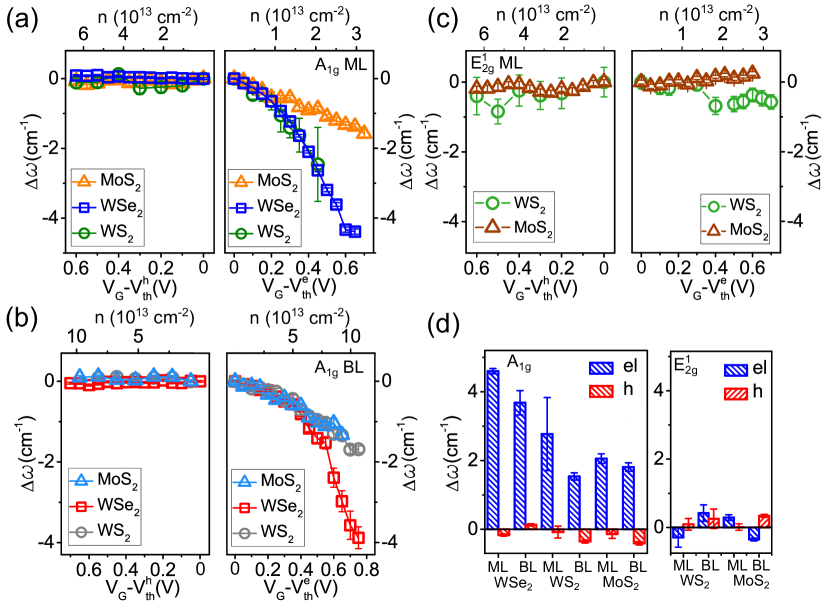
Fig. 2 reveals a number of clear trends of the Raman active modes in WSe2 monolayer and WS2 bilayer, such as the insensitivity of all phonon modes to hole accumulation, and the softening of out-of-plane modes upon electron accumulation. We have performed gate-dependent Raman spectroscopy measurements on mono and bilayers of WSe2, WS2 and MoS2 following a procedure identical to the one described here above for WSe2 monolayer and WS2 bilayer, and found that these trends are generically present in all the investigated atomically thin crystals of semiconducting TMDs. To illustrate and compare quantitatively the results of measurements performed on different systems we plot for each one of them the change in the frequency of the different phonon modes relative to the value measured at threshold for electron or hole accumulation (i.e., for each system we plot versus and ). The results of these measurements for the A1g modes in all the investigated mono- and bilayers are summarized in Fig. 3(a) and 3(b). The data for the E2g modes in monolayers are shown in Fig. 3(c). It is clear from this systematic experimental analysis –which goes well beyond what had been done until now chakraborty_symmetry-dependent_2012 ; lu_gate-tunable_2017 – that the same behavior is common to all atomically-thin TMDs.
To quantify the strength of the influence of electron and hole accumulation on the frequency of the different phonons, we plot for all systems investigated the frequency shift of the A1g and E2g modes measured at the highest value of applied gate voltage applied (relative to the corresponding threshold voltage), V, for which we have obtained data for both mono and bilayer, as well as for electron and hole accumulation. Fig. 3(d) demonstrates clearly that, for both mono and bilayers, only Raman active phonon modes with an out-of-plane component of the atomic displacement are influenced by the presence of charge carriers, whereas the E2g mode –for which the atomic displacement is in-plane– is left unaffected by the presence of free charge. The data also make the strong electron-hole asymmetry in the softening of the out-of-plane modes very apparent for all the different TMDs investigated. The order of magnitude of the effect –which is what we discuss here– is the same in all cases, corresponding to a shift of 2-4 cm-1 for the A1g optical Raman mode (for a more detailed quantitative analysis it should be recalled that –since the value of the capacitance used is different for mono and bilayers and for electron and hole accumulation– the same value of gate voltage relative to threshold does not correspond to the same carrier density capa ).
III Theoretical analysis
The experiments discussed in the previous section show unambiguously that a strong electron-hole asymmetry in the softening of the phonon frequency is a generic property of atomically thin semiconducting TMDs. The microscopic mechanism at the origin of this asymmetry, however, is not known and, especially for monolayers, finding such a pronounced asymmetry is unexpected. Indeed, the low-energy electronic states in WSe2, WS2, and MoS2 monolayers at the bottom of the conduction band and at the top of the valence bands –centered around the K/K’ points– are often described in terms of massive Dirac fermions, a conceptual framework that may lead one to expect a high degree of symmetry in the physical response upon accumulation of electrons and holes. Even though the very different strength of spin-orbit interaction in the conduction and valence band limits the validity of these considerations, whether and how spin-orbit interaction can cause such a strong asymmetry in the phonon properties upon electron and hole accumulation is very far from obvious.
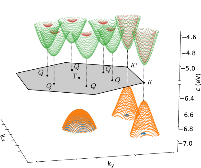
The purpose of this section is to present a theoretical analysis showing that the strength of the electron-phonon interaction in atomically-thin semiconducting TMDs is governed by whether or not multiple valleys (the and K valleys in the valence band and the K and Q valleys in the conduction band, see Fig. 4) are simultaneously populated by the accumulated charge carriers. In other words, it is the rather different valley structure of the conduction and the valence bands that is ultimately responsible for the difference in the coupling to phonons of electrons and holes, and that causes the observed electron-hole asymmetry in the softening of the phonon frequencies. In this regard, spin-orbit interaction does play a prime role, because its strongly asymmetric strength between valence and conduction bands governs the energetic alignment of the different valleys, and therefore determines whether –at any given value of carrier density– one or multiple valleys are populated.
This conclusion is based on DFT and density-functional perturbation theory (DFPT) calculations, which provide an extremely powerful tool to identify all trends in the observed dependence of the phonon frequency on the density of accumulated charge. DFT, however, cannot reproduce the experiments at a detailed quantitative level. This is because a full quantitative agreement would require a precise prediction of the relative energetic alignment of the valleys present in the valence and conduction band, which is well-known to be extremely sensitive to multiple parameters MolinaSanchez2015 ; Le2015 ; Kormanyos2015 ; Yuan2016 , from the choice of exchange-correlation functional to details of the crystal structure. Indeed, even experimental attempts to determine precisely the energetics of the different valleys seem to give scattered results, depending –for instance– on the substrate employed in the experiments (see Table 1). The situation is even more complex for bilayers, where the electric field associated with the FET doping influences the relative energy of the valleys in a way that cannot be precisely predicted at this stage. As such, our analysis aims exclusively at exploiting the possibility to tune parameters and conditions in the controlled environment of DFT simulations to identify the physical processes that explain our experimental results, and not at reproducing in quantitative detail the observed carrier density dependence of the phonon frequencies. That is also why –in view of the subtle effects caused by the gate electric field in bilayers– we focus our theoretical analysis exclusively on TMD monolayers.
To start discussing the effect of the accumulated carrier density on the phonons, we note that the softening observed in the experiments is expected when describing electron-phonon interactions within the Born-Oppenheimer approximation. In such an approximation scheme, electrons are assumed to follow the ionic motion, remaining at all times in the ground state corresponding to the instantaneous lattice configuration. This implies that phonons can be considered as static perturbations acting on the electrons, which in turn affect the vibrational properties of the system. In this regime, the expression for the change in frequency of a phonon at with respect to the neutral semiconducting case reads (see appendix B and Refs. Lazzeri2006 ; Saitta2008 ; Calandra2010 ):
| (1) |
Here we assume the limit of zero temperature, is the density of states at the Fermi energy, , and is the screened electron-phonon coupling (squared) for the -th phonon mode averaged over Fermi surface (see Eq. (B9) in appendix B). It follows that softening () is expected for phonon modes that are strongly coupled with the electronic states on the Fermi surface, whereas no frequency shift is expected for modes with a negligible electron-phonon coupling. For instance, this is the case of the pure E2g longitudinal optical mode, which affects electrons by generating a long-range scalar potential (known as Fröhlich interaction) that in the presence of free carriers (either electrons or holes) is perfectly screened in the long-wavelength limit, so that .
The assumption that carriers follow the ionic motion remaining in the instantaneous ground state implies that the Born-Oppenheimer approximation is a good description only for systems that are in the adiabatic limit. This requires the phonon energy to be much smaller than the carrier relaxation rate (), where is the carrier momentum-relaxation lifetime. In ionic-liquid gated FETs based on monolayer semiconducting TMDs the value of can be estimated from the experimentally determined carrier mobility that –under the conditions of the experiments (i.e., with ionic-liquid gated devices)– is typically 15 cm2/Vs for both electrons and holes. When compared to the characteristic phonon frequencies probed in our experiments, the resulting value of 10 fs gives . The condition to treat electron-phonon interaction in monolayer TMDs using the Born-Oppenheimer approximation is therefore fairly well satisfied at room temperature. Note also that, even when , theory allows the phonon softening to be estimated as Maksimov1996 ; Marsiglio1992 ; Saitta2008 :
| (2) |
where is given by Eq. (1). It follows directly from this expression that in the regime of our experiments the shift of the phonon frequency upon accumulation of charge carriers is correctly captured by the value in the fully adiabatic limit within a factor of two.
| (meV) | |||
|---|---|---|---|
| MoS2 | WS2 | WSe2 | |
| Exp. | 15059, 310 60; 54 | 51061, 24062,30063 | 56064, 50065, 89052 |
| DFT (this work) | 60 | 230 | 490 |
The validity of the adiabatic Born-Oppenheimer approximation makes DFT ideally suited to calculate the phonon frequency as a function of carrier density, because in DFT calculations the ground-state density is obtained by keeping the ionic positions fixed. We thus first investigate which phonon modes are sensitive to accumulation of charge carriers by computing phonon dispersions of neutral, electron-doped and hole-doped monolayer TMDs using DFPT Baroni2001 . Since simulations require overall charge neutrality, the accumulated charge is compensated by the presence of gate electrodes, and the correct boundary conditions for 2D materials are provided by cutting off the Coulomb interactions in the direction perpendicular to the layers Sohier2017 . In these initial calculations, spin-orbit coupling is not included and a relatively large electronic temperature is used to smear the Fermi surface (see methods in appendix A).
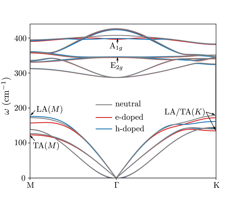
Representative DFPT results are shown in Fig. 5 for WS2. When a finite density of carriers is included, we observe a softening in various branches at several phonon wave vectors. In particular, we see that the A1g mode softens at both for electron and hole accumulation, and at M for electron accumulation only. Similarly, the frequencies of the in-plane acoustic modes (LA and TA) decrease at K both upon electron and hole accumulation, and at M exclusively for electron accumulation. On the contrary, the E2g mode remains unaffected. For all the phonon modes detected in the experiments, therefore, the simulations succeed in reproducing which modes are affected by the accumulation of charge carriers, and correctly captures the fact that carrier accumulation causes softening of the phonon frequencies. However, the overall agreement between calculations and experiments is poor. The magnitude of the softening is largely overestimated, well beyond the factor accounting for deviations from the purely adiabatic approximation of DFT. In addition, softening appears also upon hole-doping for the A1g mode at , in contrast with the experimental results.
To investigate the origin of the discrepancy between measurements and simulations, we focus our attention on the A1g which is characterized by an out-of-plane displacement of the chalcogen atoms as illustrated in Fig. 1(b) 2LAm . We computed the A1g frequency at as a function of carrier density using a finite-difference DFT scheme (see appendix A) for the three monolayer TMDs investigated here. At this stage, we made calculations more realistic by including spin-orbit coupling through fully-relativistic pseudopotentials, and by describing the occupation of electronic states according to the room-temperature Fermi-Dirac distribution (for which we made a much denser sampling of the Brillouin zone). Again, all calculations of total energy and forces include a cutoff of the Coulomb interaction to implement the correct periodic boundary conditions, and gates to maintain overall charge neutrality and properly simulate a FET configuration.
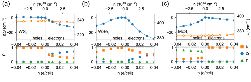
Results for monolayers of the three different TMDs investigated experimentally are shown in Fig. 6, both for electron and hole accumulation, in a range of carrier densities comparable to that explored in the experiments. In contrast to the very systematic results of the Raman measurements (see Fig. 3), the evolution of the calculated phonon frequency upon electron and hole accumulation is different for the individual TMDs, and appears at first sight to offer no systematics. In particular, we find that for WS2 (Fig. 6(a)) a large softening occurs on the electrons side, but the A1g mode frequency decreases also upon hole doping (see also Fig. 5). For WSe2 (Fig. 6(b)) instead a significant softening is present only for electrons and not for holes, whereas the opposite is true for MoS2 (Fig. 6(c)). Despite this seemingly erratic behavior, we succeeded to identify common trends enabling a rationalization of the results of the calculations. To this end, it is essential to realize that the nature of the electronic states involved plays an important role, because the softening of the phonon frequencies arises from the coupling of phonons with electrons on the Fermi surface (see Eq. (1)). That is why in the bottom panels of Fig. 6 we also plot how charge carriers in the different TMD monolayers are distributed among the relevant valleys at K, Q and (see Fig. 4), by showing their fractional occupation .
A comparison of the evolution of the phonon frequency with the population of the different valleys does indeed reveal a systematic behavior common to monolayers of all different TMDs, which holds true for both electron and hole accumulation. In all cases a strong softening of the A1g mode occurs only when two inequivalent valleys are simultaneously occupied, whereas the frequency of this mode remains constant whenever the accumulated carriers occupy exclusively one of the valleys. Specifically, the rapid decrease of the A1g frequency upon electron doping in WS2 and WSe2 originates from the simultaneous occupation of the K and Q valleys (see orange squares and blue circles in the bottom panels of Fig. 6 (a) and (b), respectively). Consistently with this idea, in MoS2 only the K-valley is populated, and no significant softening is observed. Analogous trends can be seen upon hole accumulation: A large softening is present in MoS2, for which the K and valleys are simultaneously occupied, whereas no softening is visible in WSe2 where holes populate only the K valley (see Fig. 6(c) and (b), respectively). The case of WS2 monolayers (Fig. 6(a)) confirms once more the underlying notion. In this case, the frequency of the A1g mode is insensitive to hole doping for small concentrations –when only the K valley is occupied– and starts to soften past 0.02 holes/unit cell, when holes begin to populate both the K and the valley. In all cases a very pronounced softening –larger than 10 cm-1 at cm-2– is always seen when two distinct valleys are populated, whereas whenever only one valley is populated the change in phonon frequency is typically at least one order of magnitude smaller.
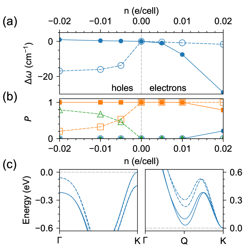
It follows from these considerations that the energy separation between valleys, which governs their relative occupation, plays an essential role in determining the magnitude of the shift in phonon frequencies (i.e., the strength of the electron-phonon coupling) upon carrier accumulation. To confirm this conclusion –and to provide further support for the effect of multivalley populations– we have performed additional calculations exploiting the extreme sensitivity of TMDs’ band structures to the in-plane lattice parameter and the vertical positions of the chalcogen atoms Yuan2016 . The goal of these calculations is to artificially tune the energy separation between valleys in order to check whether, as we expect, the softening of the A1g mode is affected significantly. We have analyzed the behavior of MoS2 monolayers using the experimentally-reported crystal structure (rather than the fully relaxed one obtained by minimizing forces and stresses at the DFT level), for which the energy separation between the K and valleys in the valence band increases from 60 meV to 220 meV (see Fig. 7(c)), and the energy difference between the K and Q valleys in the conduction band decreases from 230 meV to 30 meV. To reduce the spurious effects of thermal broadening in these calculations, we intentionally determine band occupations by using a cold-smeared distribution Marzari1999 with K, instead of a broad Fermi-Dirac distribution at K as above.
The outcome of the calculations is illustrated in Fig. 7, where we compare the carrier-density dependence of (a) the frequency of the A1g mode and (b) the fractional valley occupations obtained with either the DFT-relaxed structure (empty symbols, see also Fig. 6(c)) or the experimentally-reported one (full symbols). It is apparent that the results are distinctly different in the two cases. Upon hole accumulation a large frequency shift and a simultaneous population of the K and valleys are present for calculations performed using the DFT-relaxed structure. In contrast, no shift in frequency occurs in the calculations performed with the experimentally-reported crystal structure, where the fractional occupation of the K valley remains equal to one, i.e. only the K valley is populated. This is exactly the behavior that we would have anticipated as a result of the increased for the experimentally-reported crystal structure. Consistently, the reduction in (see Fig. 7(c)) in the experimentally-reported structure leads to a non-negligible occupation of the Q valley in addition to the lowest-lying K valley, causing a very large enhancement of the A1g softening upon electron accumulation.
We therefore conclude that the scenario hypothesized above is correct: for all monolayers investigated here, and for both electron and hole accumulation, a very sizable softening of the A1g mode occurs only when charge carriers populate multiple inequivalent valleys. Through Eq. (1), this directly implies that also the strength of the electron-phonon coupling for the A1g mode in semiconducting TMDs is large only when two valleys are occupied. This conclusion is particularly interesting because such a strong dependence of the electron-phonon coupling strength on the population of multiple inequivalent valleys in an individual band had not been identified earlier. It is nevertheless extremely likely that this mechanism is at play in many other material systems besides semiconducting TMDs, and relevant to explain a variety of physical phenomena (see, e.g., the discussion of superconductivity in section IV).
The insight gained on the importance of the simultaneous occupation of multiple valleys can now be exploited to discuss in more detail the results of our Raman spectroscopy experiments (see Fig. 3). To start with, the complete absence of phonon softening upon hole accumulation indicates that is sufficiently large in TMD monolayers to avoid the partial occupation of the valley (in addition to the dominant K valley), for hole concentrations as large as cm-2. According to the same logic, the phonon softening observed upon electron accumulation indicates that in the conduction band is sufficiently small, so that –at room temperature– both the K and Q valleys are populated in monolayers of all TMDs upon accumulation of electrons per unit cell. Additionally, it is clear from Fig. 3(a) that phonon softening upon electron accumulation is much more pronounced in W-based TMD monolayers, indicating that is smaller for WS2 and WSe2 than for MoS2.
All these conclusions are fully consistent with what is known about monolayers of semiconducting TMDs. The energy difference reported in Tab. 1 from ARPES measurements is consistent with having only the K valley occupied upon accumulation of a density of holes reaching up to cm-2 Zhang2016 ; Gao2017 ; Katoch2018 . Similarly, although no sufficiently systematic ARPES study of the conduction band of monolayer TMDs has been reported yet, analogous measurements on the doped surface of bulk TMDs (where doping should be limited to the first few layers) have shown Kang2017 that it is relatively easy to populate both the K and Q valleys in the conduction band (i.e., in monolayer TMDs is significantly smaller than ). Moreover, the observation of a larger softening in W-based monolayers, associated with the K and Q valleys being closer in WS2 and WSe2 than in MoS2, is compatible with the fact that is largely controlled by spin-orbit coupling (stronger in W-based compounds).
These considerations also make clear why the strong sensitivity of the phonon frequencies to the precise energy separation between valleys severely affects the ability of DFT to make reliable quantitative predictions. In particular, the spurious softening predicted on the hole side of MoS2 (see Fig. 6(c)) originates from the large underestimation of in DFT as compared to experiments (see Tab. 1), which leads to an erroneous occupation of both the K and valleys even at very small doping concentrations at room temperature. Something similar, although not as severe, happens also for WS2, for which the DFT prediction for is not much smaller than the experimental results in Tab. 1, but it is still sufficient to lead to a spurious softening at large hole doping. Finally, the discrepancy with experiments might arise also from a partial failure of DFT in accounting for band-structure renormalization effects that influence the doping dependence of and .
IV Discussion
Finding that the strength of the coupling of electrons to phonons is drastically amplified when multiple inequivalent valleys in a given band are populated is a phenomenon that had not been identified in the past, and it is important to build a robust physical understanding. To this end, recall that electron-phonon coupling can be qualitatively understood by considering how the band structure is perturbed by the displacement pattern of the ions associated to the phonon under consideration Bardeen1950 ; Schockley1950 ; Khan1984 . Fig. 8 shows the effect of the A1g mode on the band structure of undoped monolayer MoS2 (for better clarity, spin-orbit coupling is not included; we checked that this has no qualitative consequences on the arguments here below). Although the amplitude (up to 0.12 Å) of the A1g mode has been intentionally exaggerated with respect to typical room-temperature mean-square displacements to illustrate this effect, the large variation of both the valence and conduction bands signals the presence of a very strong electron-phonon coupling. This strength can be quantified by taking the first derivative of the band energy reported with respect to the atomic displacement, which is proportional to the bare electron phonon coupling for that band (see the right panel of Fig. 8).
The introduction of free carriers –in our experiments by means of field-effect doping– allows for the possibility of electrostatic screening, and generically tends to decrease the strength of the electron-phonon coupling (as discussed in Section I). In a simple Thomas-Fermi picture, whether or not the bare electron-phonon coupling is screened effectively by the free carriers depends on whether the evolution of the band induced by the phonon displacement pattern leads to a spatial variation of the density of charge carriers. In this regard, the situation can be very different depending on whether one or more valleys are populated.

To understand why, consider a phonon near () as a frozen atomic displacement with very long, but finite, wavelength. The static displacement associated to such a phonon shifts the valleys up and down in energy locally in space, following the local amplitude of the long-wavelength A1g mode. In the adiabatic limit, the population of the electronic states will change to keep the system in the lowest energy state. Now, if only a single valley is occupied (say the K valley in the conduction band), the only possibility for the free carriers is to follow the spatially varying position of the bottom of the valley to keep the Fermi level constant (or more appropriately the electrochemical potential, since we are considering the atomic displacement as frozen). This implies a spatial variation of the charge of the free carriers that self-consistently screens the potential of the lattice displacement, thereby strongly suppressing electron-phonon coupling.
When at least two valleys are occupied, the situation can be very different if the atomic displacements associated with the phonon mode lead to a relative out-of-phase energy shift. This is indeed so in monolayer TMDs for the Q and K valleys in the conduction band and for the K and valley in the valence band (see Fig. 8). In this case, in the presence of the atomic displacement (and when electrons/holes have the time to relax their energy and momentum during the phonon perturbation, i.e. in the adiabatic limit) charge transfer between the valleys must also occur locally in real space for the system to stay in the ground state. Since part of the charge is now involved in this “local” process, the charge that can be displaced to screen the spatially varying potential generated by the phonon is reduced, hindering the effectiveness of screening. In other words, in the presence of two valleys that shift out-of-phase in response to long-wavelength phonon excitations, screening becomes much less effective in reducing the strength of the electron-phonon coupling.
This is the main mechanism responsible for the strong softening of the A1g mode that we observe in the Raman measurements in all cases when two valleys are simultaneously occupied. For this mechanism to have a strong effect, it is essential that the phonon mode considered causes an out-of-phase shift in the the energy of the two valleys, because this maximizes the amount of inter-valley charge transfer that occurs locally in real space. For the E2g mode detected in our Raman measurements on semiconducting TMDs, for instance, this is not the case: the long-range Fröhlich potential associated with the E2g phonon near shifts the energy of the two valleys in the same direction and by comparable amounts so that no (or minimal) inter-valley charge transfer occurs locally. As a result, despite the presence of multiple inequivalent valleys, the response of the system to E2g phonons is similar to the canonical case with one single valley populated, with a strong electrostatic screening that suppresses the electron-phonon coupling.
It follows from these considerations that the underlying physical processes responsible for the enhancement of electron-phonon coupling in the presence of simultaneously populated inequivalent valleys is of quite general validity. As such, it is likely to occur in a multitude of materials and to have different experimental manifestations. It is quite remarkable that such a mechanism had not been identified earlier. We believe that this is because the analytic theoretical models commonly employed to treat electron-phonon interaction consider only one family of carriers (i.e., one single valley) coupled to phonons, and in these models the mechanism is simply not present.
Superconductivity provides an example of a physical phenomenon for which the enhanced electron-phonon coupling mechanism that we have identified may be at play. It appears that much of the existing data on gate-induced superconductivity observed in some of the TMDs (e.g., WS2 and MoS2) is consistent with having the superconducting instability setting in only when multiple valleys are occupied. Having multiple valleys occupied would explain, for instance, why gate-induced superconductivity in WS2 starts occurring at a lower electron density than in MoS2 ye_superconducting_2012 ; lu_full_2018 ; costanzo_gate-induced_2016 , because, as we discussed here above, the energy difference between the K and Q valley is smaller in WS2 than in MoS2. It also explains why so far gate-induced superconductivity in semiconducting TMDs has been observed only upon electron accumulation and not with holes ye_superconducting_2012 ; jo_electrostatically_2015 : this is because with the hole concentrations that can be reached by field-effect doping only the K or valleys are filled, so that the strength of the electron-phonon coupling remains weak. Indeed, in NbSe2 –a metal having a similar valence band structure as WS2 and MoS2, but the Fermi level very deep relative to the top of the valence band Lebegue2009 ; Nakata2018 – robust superconductivity is observed Ugeda2016 ; Xi2016 ; Tsen2016 and both the K and the valleys are occupied. The multi-valley mechanism responsible for the enhancement of the electron-phonon coupling is likely at play for other superconducting materials, with MgB2 providing a notable example. Indeed, also in MgB2 multiple inequivalent valleys are known to be simultaneously occupied and to move out-of-phase in energy when atoms are displaced according to a specific phonon pattern An2001 . More work is needed to fully substantiate the relevance of multivalley population for the occurrence of superconductivity in all these systems, but the known experimental phenomenology does provide significant circumstantial evidence supporting such a scenario.
V conclusions
In conclusion, we have identified a strong and systematic electron-hole asymmetry in the vibrational properties of mono and bilayers of semiconducting TMDs, by performing Raman measurements on ionic-liquid-gated transistors. The experiments very systematically show that, in these systems, out-of-plane modes –such as the A1g mode near zone center– soften significantly as the concentration of free electrons in the conduction band is increased, while they are left unaffected upon hole accumulation. By performing a theoretical analysis based on first-principles simulations, we have revealed that the phonon softening originates from a previously unidentified mechanism that amplifies pronouncedly the strength of electron-phonon coupling when two inequivalent valleys are simultaneously populated. This mechanism explains the asymmetry in phonon softening observed experimentally in the Raman spectroscopy measurements as due to a much larger energy separation between valleys in the valence bands as compared to the conduction band. As a result, in the range of carrier densities accessed in the experiments, simultaneous occupation of multiple valleys occurs only upon electron accumulation and not for holes.
It is surprising that this mechanism had not been identified earlier. This is most likely due to the fact that analytic theoretical models used in the discussion of electron-phonon interactions commonly treat the case of a single family of carriers (i.e., a single valley) that is coupled the lattice vibrations. It is nevertheless clear from our discussion that the microscopic processes responsible for the enhancement of electron-phonon interaction in multi-valley systems are physically robust. Hence, the same mechanism should be at play in many different material systems (i.e., not only in semiconducting transition metal dichalcogenides), and manifests itself in a variety of physical phenomena. This is likely the case, for example, of superconductivity. Existing experiments on transition metal dichalcogenides appear to indicate that the occurrence of superconductivity –either gate-induced in MoS2 and WS2, or intrinsically present in NbSe2– correlates systematically with having multiple valley populated. Similar considerations can be made for other materials, with the case of MgB2 being particularly notable. These examples underscore how the identification of a previously unappreciated mechanism enhancing the strength of electron-phonon interaction can have an important impact in the interpretation of many different phenomena observed experimentally.
Acknowledgements.
We sincerely thank Francesco Mauri, Matteo Calandra, Haijing Zhang, and Jérémie Teyssier for fruitful discussions. We gratefully acknowledge Alexandre Ferreira for continuous and precious technical support. A.F.M. gratefully acknowledges financial support from the Swis National Science Foundation (Division II) and from the EU Graphene Flagship project. M.G. and N.U. acknowledge support from the Swiss National Science Foundation through the Ambizione program. Simulation time was provided by CSCS on Piz Daint (project ID s825) and by PRACE on Marconi at CINECA, Italy (project ID 2016163963).Appendix A Methods
Te realization of the field-effect transistors used to perform the experiments described in the main text relies on a combination of conventional nanofabrication processes and of techniques that are commonly employed to manipulate atomically thin crystals, i.e. 2D materials. Monolayers and bilayers of MoS2, WS2 and WSe2 are obtained by mechanical exfoliation of bulk crystals and transferred onto Si/SiO2 substrates. The layer thickness is identified by looking at optical contrast under an optical microscope, and confirmed by photoluminescence measurements. To attach electrical contacts to the atomically thin layers, a conventional process based on electron-beam lithography, electron-beam evaporation and lift-off is used (together with the electrodes, also a large side gate electrode is deposited). The contacts consist of Pt/Au evaporated films for WSe2 and Au evaporated films for WS2 and MoS2, and are annealed at 200C in a flow of Ar:H2 gas (100:10 sccm). As a last step, the ionic liquid is drop-casted on top of the structure and confined under a 50 m thick glass plate to ensure a sharp optical image during the optical measurements. As rapidly as possible after depositing the liquid, the device is mounted in the vacuum chamber with optical access (Cryovac KONTI cryostat) where the measurements are performed (p 10-6 mbar). The devices are left under vacuum at least overnight prior to the application of any gate bias to ensure that moisture or oxygen possibly present are pumped out of the system. The ionic liquid used in all experiments is 1-butyl-1-methylpyrrolidiniumtris(penta-fluoroethyl) trifluorophosphate [P14][FAP]. All measurements discussed here have been performed at room temperature; at lower temperature the same procedure cannot be applied because of freezing of the [P14][FAP] ionic liquid.
The Raman scattering spectroscopy measurements are performed using a home tailored confocal microscope in a back-scattering geometry, i.e. collecting the emitted light with the same microscope used to couple the laser beam (at 514.5 nm) onto the device (see Fig. 1c for a sketch of the experimental setup). The Back-scattered light is sent to a Czerni-Turner spectrometer equipped with a 1800 groves/mm grating which resolves the optical spectra with a precision of 0.5 cm-1. The light is detected with the help of a N2-cooled CCD-array (Princeton Instruments). In the experiments, the gate voltage is slowly swept from positive to negative values. At VG intervals of 0.2 V the sweep is interrupted and Raman spectra are recorded at fixed VG values. After reaching the largest negative gate voltage, VG is swept back to positive values, and spectra are again recorded at fixed intervals to ensure that the experimental data are free from hysteresis. Finally, we have checked that the ionic liquid does not possess any characteristic Raman feature in the spectral range of interest.
DFT calculations are performed using Quantum ESPRESSO Giannozzi2009 ; Giannozzi2017 , including a cutoff of the Coulomb interaction to implement the correct boundary conditions and gates to simulate doping Sohier2017 . We use a symmetric double-gate geometry; for monolayers a single-gate geometry leads to minimal changes on the results. The exchange-correlation functional is approximated using the Perdew-Burke-Ernzerhof (PBE) form PBE of the generalized-gradient approximation. To compute full phonon dispersions, we use the SSSP Accuracy library prandini_standard_2018 ; Prandini2018 (version 0.7), a Ry energy cutoff, and a grid with Ry Marzari-Vanderbilt broadening Marzari1999 . We then use density-functional perturbation theory Baroni2001 –including Coulomb cutoff and gates– to compute the phonons on a grid in the Brillouin zone. For zone-center phonon calculations, we significantly reduce smearing and increase the sampling accordingly: Namely, we use a dense k-point grid and Fermi-Dirac smearing corresponding to room temperature (0.002 Ry). Spin-orbit interaction is included by using fully relativistic norm-conserving pseudopotentials from the Pseudo-Dojo library vanSetten2018 . Phonopy Togo2015 is then used to generate the atomic-displacement patterns and to post-process forces to obtain phonon frequencies.
Appendix B Justification of Eq. (1) in the main text
In the the following, we show how to use expressions derived in Refs. Lazzeri2006 ; Saitta2008 ; Calandra2010 to obtain Eq. (1) with the help of few assumptions valid in the case of semiconducting TMDs. We are interested in the doping-induced frequency variations of a phonon mode at (phonon momentum ) with respect to its value in the neutral case . The frequency of a given phonon mode corresponding to an eigenvector of the dynamical matrix at , , can be obtained as , where is an effective mass associated with the phonon mode and is the projection of the dynamical matrix on the corresponding eigenvector or equivalently of the force constants on the physical displacements of the phonon mode (with ). Assuming that the variation of the frequency is small compared to the neutral frequency , we can differentiate () to obtain the following simple relation:
| (B1) |
Neglecting the variations with doping of the contributions from the second-order derivatives of the ionic potential and the exchange-correlation kernel with respect to the atomic displacements in Eq. (3) of Ref. Saitta2008 , we write:
| (B2) |
where is the part of the dynamical matrix at the point involving the electronic response to the phonon perturbation, and thus electron-phonon interactions. The explicit expression for depends on the adiabaticity of the system. In the adiabatic limit relevant for TMDs, it reads Saitta2008 ; Lazzeri2006 ; Calandra2010 :
| (B3) | ||||
| (B4) |
where is the perturbation of the effective potential due to phonon , is the occupation of the state corresponding to the band at crystal momentum with energy . In the first term, there are only interband contributions () between occupied and empty states. We have verified that the numerator is much smaller than the denominator , which is equal to the direct gap in the neutral case, so that this term can be neglected. The second term involves intraband transitions between states close to the Fermi surface and it is non-zero only in doped systems, while vanishing in neutral TMDs. This is the main contribution to doping-induced variations, so that we can write:
| (B5) |
where we have introduced the square electron-phonon matrix element due to intraband transitions:
| (B6) |
The derivative of the Fermi distribution is negative (the phonon frequency softens) and non-zero only in a small energy window of order around the chemical potential, so that only electronic states belonging to the temperature-smeared Fermi surface contribute. In the zero temperature limit the derivative becomes a delta function at the Fermi energy and we obtain
| (B7) |
which is Eq. (1) of the main text. Here we have introduced the density of states at the Fermi energy
| (B8) |
and the square electron-phonon coupling averaged over the Fermi surface:
| (B9) |
References
- (1) J. M. Ziman, Electrons and phonons: the theory of transport phenomena in solids (Clarendon, Oxford, 1960).
- (2) G. Grimvall, The electron-phonon interaction in metals (North-Holland, Amsterdam, 1981).
- (3) G. D. Mahan, Many-Particle Physics, 3rd ed. (Plenum, New York, 2000).
- (4) J. Bardeen and W. Shockley, Phys. Rev. 80, 72 (1950).
- (5) W. Shockley and J. Bardeen, Phys. Rev. 77, 407 (1950).
- (6) L. Pietronero, S. Strässler, H. R. Zeller, and M. J. Rice, Phys. Rev. B 22, 904 (1980).
- (7) T. Sohier, M. Calandra, C.-H. Park, N. Bonini, N. Marzari, and F. Mauri, Phys. Rev. B 90, 125414 (2014).
- (8) M. Vozmediano, M. Katsnelson, and F. Guinea, Physics Reports 496, 109 (2010).
- (9) S. Engelsberg and J. R. Schrieffer, Phys. Rev. 131, 993 (1963).
- (10) E. Maksimov and S. Shulga, Solid State Communications 97, 553 (1996).
- (11) P. Bogulsawski and J. Mycielski, Journal of Physics C: Solid State Physics 10, 2413 (1977).
- (12) F. S. Khan and P. B. Allen, Phys. Rev. B 29, 3341 (1984).
- (13) E. Kartheuser and S. Rodriguez, Phys. Rev. B 33, 772 (1986).
- (14) A. C. Ferrari, Solid State Communications , Exploring graphene143, 47 (2007).
- (15) A. C. Ferrari and D. M. Basko, Nature Nanotechnology 8, 235 (2013).
- (16) S. Pisana, M. Lazzeri, C. Casiraghi, K. S. Novoselov, A. K. Geim, A. C. Ferrari, and F. Mauri, Nature Materials 6, 198 (2007).
- (17) D. A. Kirzhnits, E. G. Maksimov, and D. I. Khomskii, Journal of Low Temperature Physics 10, 79 (1973).
- (18) J. L. M. van Mechelen, D. van der Marel, C. Grimaldi, A. B. Kuzmenko, N. P. Armitage, N. Reyren, H. Hagemann, and I. I. Mazin, Physical Review Letters 100, 226403 (2008).
- (19) Z. Wang, S. McKeown Walker, A. Tamai, Y. Wang, Z. Ristic, F. Y. Bruno, A. de la Torre, S. Riccò, N. C. Plumb, M. Shi, P. Hlawenka, J. Sánchez-Barriga, A. Varykhalov, T. K. Kim, M. Hoesch, P. D. C. King, W. Meevasana, U. Diebold, J. Mesot, B. Moritz, T. P. Devereaux, M. Radovic, and F. Baumberger, Nature Materials 15, 835 (2016).
- (20) C. Verdi, F. Caruso, and F. Giustino, Nature Communications 8, 15769 (2017).
- (21) T. Sohier, M. Calandra, and F. Mauri, Physical Review B 96, 075448 (2017).
- (22) J. T. Ye, Y. J. Zhang, R. Akashi, M. S. Bahramy, R. Arita, and Y. Iwasa, Science 338, 1193 (2012).
- (23) S. Jo, D. Costanzo, H. Berger, and A. F. Morpurgo, Nano Letters 15, 1197 (2015).
- (24) J. Lu, O. Zheliuk, Q. Chen, I. Leermakers, N. E. Hussey, U. Zeitler, and J. Ye, Proceedings of the National Academy of Sciences 115, 3551 (2018).
- (25) Y. Hamaue and R. Aoki, Journal of the Physical Society of Japan 55, 1327 (1986).
- (26) I. Guillamón, H. Suderow, S. Vieira, L. Cario, P. Diener, and P. Rodière, Phys. Rev. Lett. 101, 166407 (2008).
- (27) X. Xi, Z. Wang, W. Zhao, J.-H. Park, K. T. Law, H. Berger, L. Forró, J. Shan, and K. F. Mak, Nature Physics 12, 139 (2016).
- (28) M. M. Ugeda, A. J. Bradley, Y. Zhang, S. Onishi, Y. Chen, W. Ruan, C. Ojeda-Aristizabal, H. Ryu, M. T. Edmonds, H.-Z. Tsai, A. Riss, S.-K. Mo, D. Lee, A. Zettl, Z. Hussain, Z.-X. Shen, and M. F. Crommie, Nature Physics 12, 92 (2016).
- (29) A. W. Tsen, B. Hunt, Y. D. Kim, Z. J. Yuan, S. Jia, R. J. Cava, J. Hone, P. Kim, C. R. Dean, and A. N. Pasupathy, Nature Physics 12, 208 (2016).
- (30) D. Braga, I. Gutiérrez Lezama, H. Berger, and A. F. Morpurgo, Nano Letters 12, 5218 (2012).
- (31) Y. J. Zhang, T. Oka, R. Suzuki, J. T. Ye, and Y. Iwasa, Science 344, 725 (2014).
- (32) I. G. Lezama, A. Ubaldini, M. Longobardi, E. Giannini, C. Renner, A. B. Kuzmenko, and A. F. Morpurgo, 2D Materials 1, 021002 (2014).
- (33) S. Jo, N. Ubrig, H. Berger, A. B. Kuzmenko, and A. F. Morpurgo, Nano Letters 14, 2019 (2014).
- (34) N. Ubrig, S. Jo, H. Berger, A. F. Morpurgo, and A. B. Kuzmenko, Applied Physics Letters 104, 171112 (2014).
- (35) E. Ponomarev, I. Gutiérrez-Lezama, N. Ubrig, and A. F. Morpurgo, Nano Letters 15, 8289 (2015).
- (36) Y. Zhang, J. Ye, Y. Matsuhashi, and Y. Iwasa, Nano Letters 12, 1136 (2012).
- (37) D. Costanzo, S. Jo, H. Berger, and A. F. Morpurgo, Nature Nanotechnology 11, 339 (2016).
- (38) I. Gutiérrez-Lezama, B. A. Reddy, N. Ubrig, and A. F. Morpurgo, 2D Materials 3, 045016 (2016).
- (39) C. Lee, H. Yan, L. E. Brus, T. F. Heinz, J. Hone, and S. Ryu, ACS Nano 4, 2695 (2010).
- (40) A. Molina-Sánchez and L. Wirtz, Physical Review B 84, 155413 (2011).
- (41) A. Berkdemir, H. R. Gutiérrez, A. R. Botello-Méndez, N. Perea-López, A. L. Elías, C.-I. Chia, B. Wang, V. H. Crespi, F. López-Urías, J.-C. Charlier, H. Terrones, and M. Terrones, Scientific Reports 3, 1755 (2013).
- (42) H. Sahin, S. Tongay, S. Horzum, W. Fan, J. Zhou, J. Li, J. Wu, and F. M. Peeters, Physical Review B 87, 165409 (2013).
- (43) R. Saito, Y. Tatsumi, S. Huang, X. Ling, and M. S. Dresselhaus, Journal of Physics: Condensed Matter 28, 353002 (2016).
- (44) H. Terrones, E. D. Corro, S. Feng, J. M. Poumirol, D. Rhodes, D. Smirnov, N. R. Pradhan, Z. Lin, M. a. T. Nguyen, A. L. Elías, T. E. Mallouk, L. Balicas, M. A. Pimenta, and M. Terrones, Scientific Reports 4, 4215 (2014).
- (45) A. A. Mitioglu, P. Plochocka, G. Deligeorgis, S. Anghel, L. Kulyuk, and D. K. Maude, Physical Review B 89, 245442 (2014).
- (46) A. Carvalho, R. M. Ribeiro, and A. H. Castro Neto, Physical Review B 88, 115205 (2013).
- (47) The values of carrier density are estimated using values of the capacitance per unit area obtained from previous experiments (in which the capacitance was obtained using the Hall effect to measure the density of accumulated charge). These past experiments show that in ionic-liquid gated transistors on mono and bilayer semiconducting TMDS –in the range of density explored here– the capacitance value is largely determined by the density of states (i.e., taking into account the quantum capacitance is essential). Since the density of states is different for mono and bilayers and –once the thickness is fixed– for the conduction and valence bands, different values for have to be used. At room temperature, the capacitance does not depend much on the specific compound considered and here we use the values measured on WSe2 mono and bilayers, which are: C = 7.3 ; C = 17 ; C = 22.8 ; C = 24 (the subscript ML and BL refer to mono and bilayer; the superscript and indicates the value to use for accumulation of electrons and holes, respectively).
- (48) In view of the microscopic complexity of the resonant process from which the 2LA(M) Raman peak originates, and of the fact that –as it will be discussed explicitly in Section III– our main interest here is on long-wavelength phonons, we will not discuss the behavior of the 2LA(M) Raman peak. As a only remark, note that –just like for the A1g mode– the LA(M) mode corresponds to an out-of-plane motion of the atoms in the lattice, and a finite electron-phonon coupling is present, as demonstrated by the sensitivity of the mode frequency to the introduction of charge carriers.
- (49) B. Chakraborty, A. Bera, D. V. S. Muthu, S. Bhowmick, U. V. Waghmare, and A. K. Sood, Physical Review B 85, 161403 (2012).
- (50) X. Lu, M. I. B. Utama, X. Wang, W. Xu, W. Zhao, M. H. S. Owen, and Q. Xiong, Small 13, 1701039 (2017).
- (51) A. Molina-Sánchez, K. Hummer, and L. Wirtz, Surface Science Reports 70, 554 (2015).
- (52) D. Le, A. Barinov, E. Preciado, M. Isarraraz, I. Tanabe, T. Komesu, C. Troha, L. Bartels, T. S. Rahman, and P. A. Dowben, Journal of Physics: Condensed Matter 27, 182201 (2015).
- (53) A. Kormányos, G. Burkard, M. Gmitra, J. Fabian, V. Zólyomi, N. D. Drummond, and V. Fal’ko, 2D Materials 2, 022001 (2015).
- (54) H. Yuan, Z. Liu, G. Xu, B. Zhou, S. Wu, D. Dumcenco, K. Yan, Y. Zhang, S.-K. Mo, P. Dudin, V. Kandyba, M. Yablonskikh, A. Barinov, Z. Shen, S. Zhang, Y. Huang, X. Xu, Z. Hussain, H. Y. Hwang, Y. Cui, and Y. Chen, Nano Letters 16, 4738 (2016).
- (55) M. Lazzeri and F. Mauri, Phys. Rev. Lett. 97, 266407 (2006).
- (56) A. M. Saitta, M. Lazzeri, M. Calandra, and F. Mauri, Phys. Rev. Lett. 100, 226401 (2008).
- (57) M. Calandra, G. Profeta, and F. Mauri, Phys. Rev. B 82, 165111 (2010).
- (58) F. Marsiglio, R. Akis, and J. P. Carbotte, Phys. Rev. B 45, 9865 (1992).
- (59) W. Jin, P.-C. Yeh, N. Zaki, D. Zhang, J. T. Sadowski, A. Al-Mahboob, A. M. van der Zande, D. A. Chenet, J. I. Dadap, I. P. Herman, P. Sutter, J. Hone, and R. M. Osgood, Phys. Rev. Lett. 111, 106801 (2013).
- (60) J. A. Miwa, S. Ulstrup, S. G. Sørensen, M. Dendzik, A. G. c. v. a. c. Čabo, M. Bianchi, J. V. Lauritsen, and P. Hofmann, Phys. Rev. Lett. 114, 046802 (2015).
- (61) M. Dendzik, M. Michiardi, C. Sanders, M. Bianchi, J. A. Miwa, S. S. Grønborg, J. V. Lauritsen, A. Bruix, B. Hammer, and P. Hofmann, Phys. Rev. B 92, 245442 (2015).
- (62) C. Kastl, C. T. Chen, R. J. Koch, B. Schuler, T. R. Kuykendall, A. Bostwick, C. Jozwiak, T. Seyller, E. Rotenberg, A. Weber-Bargioni, S. Aloni, and A. M. Schwartzberg, 2D Materials 5, 045010 (2018).
- (63) H. Henck, Z. Ben Aziza, D. Pierucci, F. Laourine, F. Reale, P. Palczynski, J. Chaste, M. G. Silly, F. Bertran, P. Le Fèvre, E. Lhuillier, T. Wakamura, C. Mattevi, J. E. Rault, M. Calandra, and A. Ouerghi, Phys. Rev. B 97, 155421 (2018).
- (64) Y. Zhang, M. M. Ugeda, C. Jin, S.-F. Shi, A. J. Bradley, A. Martín-Recio, H. Ryu, J. Kim, S. Tang, Y. Kim, B. Zhou, C. Hwang, Y. Chen, F. Wang, M. F. Crommie, Z. Hussain, Z.-X. Shen, and S.-K. Mo, Nano Letters 16, 2485 (2016).
- (65) N. R. Wilson, P. V. Nguyen, K. Seyler, P. Rivera, A. J. Marsden, Z. P. L. Laker, G. C. Constantinescu, V. Kandyba, A. Barinov, N. D. M. Hine, X. Xu, and D. H. Cobden, Science Advances 3 (2017).
- (66) S. Baroni, S. de Gironcoli, A. Dal Corso, and P. Giannozzi, Rev. Mod. Phys. 73, 515 (2001).
- (67) N. Marzari, D. Vanderbilt, A. De Vita, and M. C. Payne, Phys. Rev. Lett. 82, 3296 (1999).
- (68) S. Gao and L. Yang, Phys. Rev. B 96, 155410 (2017).
- (69) J. Katoch, S. Ulstrup, R. J. Koch, S. Moser, K. M. McCreary, S. Singh, J. Xu, B. T. Jonker, R. K. Kawakami, A. Bostwick, E. Rotenberg, and C. Jozwiak, Nature Physics 14, 355 (2018).
- (70) M. Kang, B. Kim, S. H. Ryu, S. W. Jung, J. Kim, L. Moreschini, C. Jozwiak, E. Rotenberg, A. Bostwick, and K. S. Kim, Nano Letters 17, 1610 (2017).
- (71) S. Lebègue and O. Eriksson, Phys. Rev. B 79, 115409 (2009).
- (72) Y. Nakata, K. Sugawara, S. Ichinokura, Y. Okada, T. Hitosugi, T. Koretsune, K. Ueno, S. Hasegawa, T. Takahashi, and T. Sato, npj 2D Materials and Applications 2, 12 (2018).
- (73) J. M. An and W. E. Pickett, Phys. Rev. Lett. 86, 4366 (2001).
- (74) P. Giannozzi, S. Baroni, N. Bonini, M. Calandra, R. Car, C. Cavazzoni, D. Ceresoli, G. L. Chiarotti, M. Cococcioni, I. Dabo, A. Dal Corso, S. de Gironcoli, S. Fabris, G. Fratesi, R. Gebauer, U. Gerstmann, C. Gougoussis, A. Kokalj, M. Lazzeri, L. Martin-Samos, N. Marzari, F. Mauri, R. Mazzarello, S. Paolini, A. Pasquarello, L. Paulatto, C. Sbraccia, S. Scandolo, G. Sclauzero, A. P. Seitsonen, A. Smogunov, P. Umari, and R. M. Wentzcovitch, Journal of Physics: Condensed Matter 21, 395502 (2009).
- (75) P. Giannozzi, O. Andreussi, T. Brumme, O. Bunau, M. Buongiorno Nardelli, M. Calandra, R. Car, C. Cavazzoni, D. Ceresoli, M. Cococcioni, N. Colonna, I. Carnimeo, A. Dal Corso, S. de Gironcoli, P. Delugas, R. A. DiStasio, A. Ferretti, A. Floris, G. Fratesi, G. Fugallo, R. Gebauer, U. Gerstmann, F. Giustino, T. Gorni, J. Jia, M. Kawamura, H.-Y. Ko, A. Kokalj, E. Küçükbenli, M. Lazzeri, M. Marsili, N. Marzari, F. Mauri, N. L. Nguyen, H.-V. Nguyen, A. Otero-de-la Roza, L. Paulatto, S. Poncé, D. Rocca, R. Sabatini, B. Santra, M. Schlipf, A. P. Seitsonen, A. Smogunov, I. Timrov, T. Thonhauser, P. Umari, N. Vast, X. Wu, and S. Baroni, Journal of Physics: Condensed Matter 29, 465901 (2017).
- (76) J. P. Perdew, K. Burke, and M. Ernzerhof, Phys. Rev. Lett. 77, 3865 (1996).
- (77) G. Prandini, A. Marrazzo, I. E. Castelli, N. Mounet, and N. Marzari, (2018).
- (78) G. Prandini, A. Marrazzo, I. E. Castelli, N. Mounet, and N. Marzari, npj Computational Materials 4, 72 (2018).
- (79) M. van Setten, M. Giantomassi, E. Bousquet, M. Verstraete, D. Hamann, X. Gonze, and G.-M. Rignanese, Computer Physics Communications 226, 39 (2018).
- (80) A. Togo and I. Tanaka, Scr. Mater. 108, 1 (2015).