Tight-binding calculations of SiGe alloy nanocrystals in SiO2 matrix
Abstract
In the empirical tight-binding approach we study the electronic states in spherical SiGe nanocrystals embedded in SiO2 matrix. The energy and valley structure is obtained as a function of Ge composition and nanocrystal size. The calculations show that the mixing of hot electrons in the nanocrystal with the electrons in wide band gap matrix is possible and this mixing strongly depends on the Ge composition in the nanocrystal.
I Introduction
The SiGe alloy has the crystal structure similar to the bulk silicon and it is possible to create the Si1-xGex layers on the silicon substrate changing the content of Ge in the wide range from (pure silicon) to (pure germanium). This system is widely used in modern electronics: by changing the Ge content it is possible to switch the electronic band structure from bulk silicon to germanium. An important feature of Si1-xGex material is high mobility and convenient, well-developed production technology. These properties have opened a way of using Si1-xGex to manufacture different electronic devices: high-speed transistors,Meyerson (1994) long-wave infrared detectors,Lin and Maserjian (1990) solar cells based on p-i-n structures.Bidiville et al. (2014)
The use of silicon and germanium in optoelectronics is limited by the fundamental feature of their indirect band structure: the extrema of the conduction band are near the edge of the Brillouin zone, and the top of the valence-band is at the center of this zone. However, in nanocrystals (NCs), electrons and holes are localized and no longer have a definite (quasi)momentum due to the Heisenberg uncertainty principle. It stimulates the rapid development of technology, experimental, and theoretical work on the study of optical phenomena in silicon and germanium nanoparticles. There is a large number of reviews and monographs devoted to the successful application of silicon nanocrystals in SiO2 matrix in optoelectronics, photovoltaics and medicine (see Ref. Priolo et al., 2014).
In Ref. Takeoka et al., 2000 the photoluminescence from spherical Si1-xGex alloy nanocrystals with 4–5 nm diameter in SiO2 matrix was studied as a function of the Ge content. The samples were fabricated by the cosputtering of Si, Ge, and SiO2 and postannealing at 1100C. Recently, similar NCs prepared using the same technique were studied in details by spectroscopy and time-resolved spectroscopy.Ha et al. (2015, 2016)
In the present paper, we develop the empirical tight binding (ETB) approachJancu et al. (1998) for the modeling of electronic states and energy levels of SiGe nanocrystals embedded in SiO2 matrix and present the results of modeling for Si1-xGex nanocrystals with germanium content in wide region from to . The distributions of the density of states in reciprocal real and real space shows the X–L valley transition as a function of Ge content and also shows that excited electronic states with relatively small energy may strongly penetrate the SiO2 matrix.
II Virtual crystal approach for SiGe alloy
To simulate the alloy in empirical tight-binding (ETB), two approaches are widely used. First, one may consider the randomly chosen atom distribution within the structure and then average over realizations.Wei et al. (1990) Second option is to use the virtual crystal approximation (VCA) which is the ETB parametrization of the averaged band structure of the alloy. Second approach has its limitations: It is valid only in the cases when one wants to neglect the effects due to the disorder in the alloy material.
Recently it has been shownNestoklon et al. (2016a) that for the VCA in ETB it is not necessary to parametrize the alloy. At least for ternary alloys in the InGaAsSb and AlGaAs family the band structure of an alloy may be constructed from the ETB parameters of basic materials. Here we adopt the same procedure for the SiGe alloy. The parameters of the alloy are found from the parameters of Si and Ge: The lattice constant of the alloy is found as a linear interpolation between binaries (Vegard’s law). Then the parameters of Si1-xGex alloy are found as a linear interpolation of ETB parameters of Si and Ge strained to the lattice constant of the alloy.
In the method proposed in Ref. Nestoklon et al., 2016a it is assumed that in the parametrization of binary materials is critically important to have accurate description of the deformation potentials of basic materials, in which case the band structure of alloy will also be precise. The parametrization for bulk Si and Ge (as well as for SiGe bonds) which takes into account the change of the parameters due to strain may be found in Ref. Niquet et al., 2009.
In the ETB we follow the procedure of Ref. Jancu et al., 1998 and construct the matrix elements of the tight-binding Hamiltonian using the standard procedure.Slater and Koster (1954) The parameters also depend on the strain: First, the transfer matrix elements of bulk Si and Ge are scaled due to the change of the lattice parameter following standard generalized Harrison lawJancu et al. (1998)
| (1) |
where and the transfer parameters and lattice constant for the material (Si, Ge or SiGe), and is the power in generalized Harrison law, these parameters are taken from Ref. Niquet et al., 2009. The lattice constant of the alloy is found from the linear interpolation
| (2) |
The valence band offset (VBO) of the alloy depends linearly on
| (3) |
where (see Ref. Niquet et al., 2009).
In addition to the change of transfer matrix elements we also take into account the shift of orbital energies proportional to hydrostatic component of strain tensor
| (4) |
where parameters ( indexes the basis function of ETB) are also taken from Ref. Niquet et al., 2009.
The splitting of diagonal energies is proportional to the off-diagonal components of the strain tensor introduced in Refs. Nestoklon et al., 2016a; Niquet et al., 2009 is irrelevant to the construction of VCA alloy parameters and we do not discuss it here.
III Virtual crystal approach for SiO2 matrix
The simulation of Si1-xGex alloy nanocrystals in SiO2 by the tight-binding method is complicated by the fact that SiO2 is an amorphous material. However, at the interface between SiO2 and Si1-xGex NCs, there is a large band offset for both types of carriers and, therefore, the electron and hole wave functions rapidly damp in the matrix. In this case, the role of disorder may be neglected and the most important factors are the general band structure of material surrounding nanocrystal and the boundary conditions between Si1-xGex alloy and SiO2. It opens the possibility to simulate SiO2 as a virtual crystal.Nestoklon et al. (2016b) We construct the virtual crystal with a band structure close to the band structure of -cristobalite near the band gap edges, following Ref. Belolipetskiy et al., 2018. The -cristobalite is the only polymorphous modification with a cubic lattice among SiO2 crystals. As a target band structure we use the band structure of -cristobalite calculated from the first principles in Ref. nian Xu and Ching, 1991. As there is no strain of NCs in amorphous matrix, we set the lattice constant of the virtual crystal matching the lattice constant of the bulk Si1-xGex alloy which forms the NC. The tight-binding parameters for the virtual crystal SiO2 may be found in Ref. Belolipetskiy et al., 2018 and in appendix.
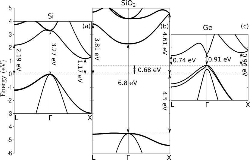
Fig. 2 demonstrates the energy position of the band edges of the bulk silicon, virtual crystal SiO2 and germanium. The virtual crystal SiO2 is the direct-band material with the band gap equal to 6.79 eV matching the value in -cristobalite, the extrema of conduction and valence band lie in the point. Bulk silicon is the indirect-band semiconductor, with the 6 minima of the conduction band located at between and points of the Brillouin zone (the distance between minima and point is 0.85 of the – distance). Bulk germanium is also an indirect-band semiconductor with 4 minima of the conduction band in points. To consider the tunneling of electrons into the SiO2 matrix, it is critical to reproduce exactly the energy positions of the edges of the conduction bands of the SiO2 in and points. The distances from the top of the valence band at the point to the points and of the conduction band for the virtual crystal are 9.11 eV and 8.31 eV, respectively, which is close to values in -cristabolite. The comparison of the band structures of the virtual crystal and -cristobalite is presented in Ref. Belolipetskiy et al., 2018. We set the top of the valence band of the bulk silicon at the energy distance 4.5 eV above the top of the valence band in virtual crystal. This corresponds to the experimental data on the valence band offset between bulk silicon and amorphous SiO2.Sze (1981)
IV Results of modeling the SiGe nanocrystal in SiO2
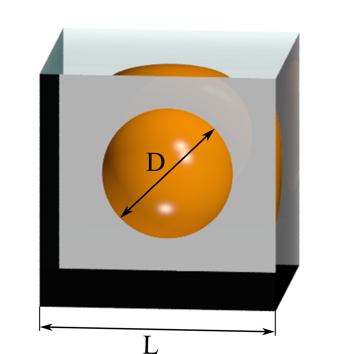
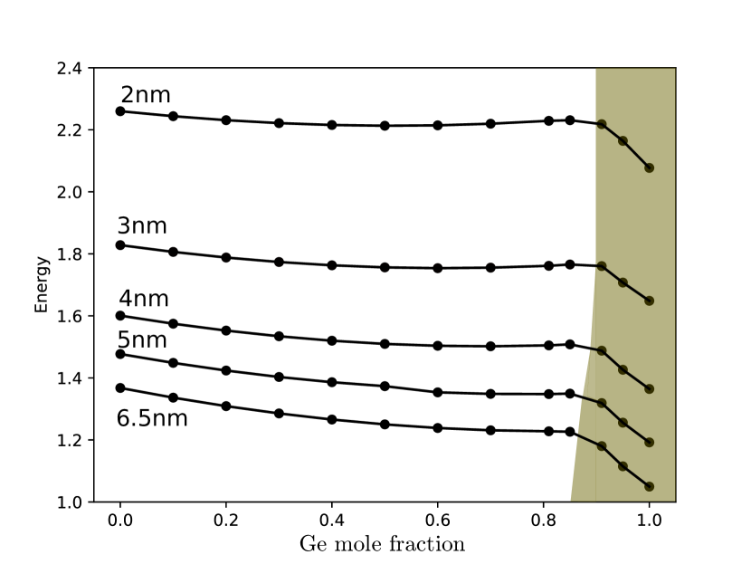
For convenience, in the calculations of electron and hole states in Si1-xGex nanocrystals embedded in the SiO2 matrix, we consider a cubic supercell of the virtual SiO2 with a Si1-xGex alloy nanocrystal in the supercell center (see Fig. 3). In calculations, we use the periodic boundary conditions to discard the effects at the surface and choose the SiO2 cell to be large enough to neglect the tunneling between neighboring NCs. The NC with diameter is constructed by placing the SiGe “atoms” inside the sphere with diameter nm. Extra 0.5 nm are added to compensate for the interface effects, similar to Ref. Seino et al., 2010. Results of calculation of the energy gap for Si1-xGex nanocrystals with diameters = 2, 3, 4, 5 and 6.5 nm as a function of Ge content are presented in Fig. 4. The value of NC diameter corresponds to the pure silicon nanocrystal (x=0). For the Si1-xGex alloy nanocrystals we consider the NCs with the same number of atoms (the diameter is larger by the factor ).
V Discussion
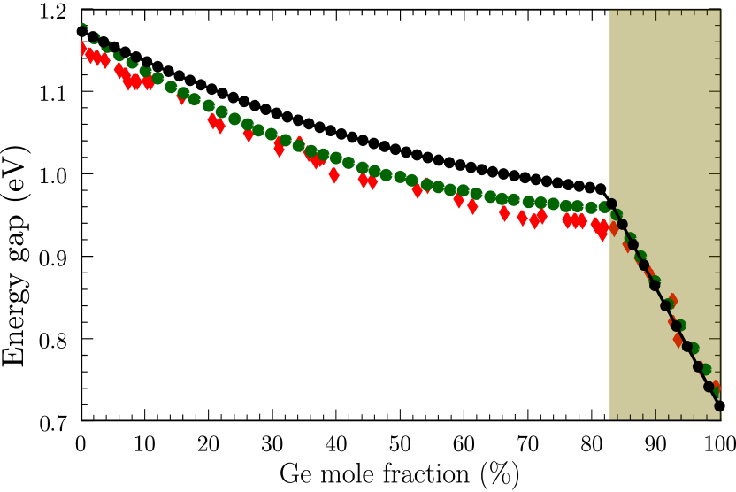
First of all, let us discuss a good agreement between the detailed model of the SiGe alloy obtained as a averaged over the realizations of the random distribution of both atoms in a large supercell and the simple virtual crystal approximation. In addition to simplicity, the VCA allows for much easier analysis of the band structure behavior, as the bulk states do not need the extra unfolding procedure to get the valley index of the states. In particular, this allows one to unambiguously attribute the shoulder in Fig. 1 to the crossover between lowest valley in SiGe alloy with low Ge content to the lowest valley in SiGe alloy with high Ge content.
The detailed analysis of the SiO2 band structure allowed us to construct the tight-binding parameters of the virtual crystal which reproduces all important features of the -cristabolite band structure. This allows one to use the atomistic tight-binding to compute the states in relatively large nanocrystals with the account on the tunneling of the states in the matrix and the valley mixing. We stress that in this case the advantage of the tight-binding method is not the detailed description of the interface properties and/or the chemistry of the contact between SiGe and SiO2 which is out of the scope of present paper, but the detailed quantitative description of the band structure of all materials in the full Brillouin zone and exact (within the model) account on the interaction between the states in different valleys.
Calculations show that the band structure of the SiGe alloy is qualitatively reflected in the quantum quantization of the states in nanocrystals. However, there are some changes. First, the position of – crossover point is shifted towards high Ge content in small NCs, see Fig. 4. Second, for small NCs the band gap dependence on the Ge content is almost absent. This may be explained by the opposed influence of the badgap change and the change of the effective mass. As a result, for intermediate size NCs the effect of the Ge content on the NC band gap is strongly suppressed, and the band gap for 2-3 nm size NCs is constant when the Ge content is within the range 0.0-0.85. We remind that the NCs in our calculations are nominally unstrained.
In Fig. 5 we demonstrate the local density of states (LDOS) for electron and hole states in real and k-spaces for nanocrystal with diameter 3 nm (number of atoms in the NC is ).
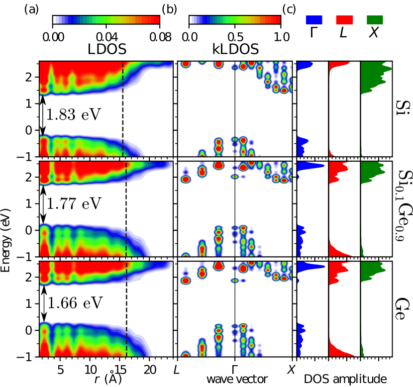
From the LDOS of the electron states it is easy to note that the close position of the conduction band in the matrix leads to the strong penetration of the hot electron states in the matrix. The interesting feature of the tunneling into matrix is that it is more “smeared” for Ge nanocrystals. Most likely, this is due to the fact that in Ge valley lies less than 300 meV above the conduction band bottom in valleys. This means that electron states inside NCs with energies 300 meV above the ground level have strong admixture of the valley, the same valley which forms the conduction band in the matrix and their tunneling is proportional to the difference between the energy of the state and the bottom of the conduction band in the matrix. As a result, the tunneling exponent is linear with the energy. However, for Si NCs the valley in the NC material lies high above, so the tunneling into matrix is defined by the - mixing at the interface which is small. Only when the energy of the electrons reaches the conduction band of the matrix, the electron starts to move freely. In Fig. 5 this is easy to see in first column: the states in purely Si NCs almost fully confined within the NC, and become completely delocalized as long as the energy of the conduction band in the matrix is reached. In NCs with high Ge content, the states start to penetrate the matrix more and more as the energy reaches the bottom of the matrix conduction band and even when this energy is reached they are still somewhat localized near the NC as long as they strongly feel the potential of the NC.
In second column of Fig. 5 LDOS in k-space shows that the states follow the band structure of the alloy. Distinct localization of the states near the k points of Brillouin zone corresponding to the position of and valleys for Ge NCs, and only valleys for Si NC. Note that the contribution to the valley for Si NCs is not from the Si itself, but due to states in the SiO2 matrix: the valley in Si lies significantly above the maximum energy shown in this figure.
Total valley-resolved DOS is shown in the three right columns in Fig. 5 also shows that for Si NCs the states are in the valley, hot electrons with energies about 1.2 eV above the ground electron state acquire significant contribution from the valley of Si and valley of the SiO2 matrix. For Si0.1Ge0.9 valley reaches valley, so the states become mixed with the valley for rather small energy, but they contribute only slightly to DOS due to the absence of valley degeneracy and rather light electron mass and for purely Ge NC valley is lowest, with and valleys close.
VI Conclusion
In conclusion, we show that the VCA description in the framework of empirical tight-binding method for SiGe alloys and SiO2 is an effective and quantitatively correct approach. The calculations of electron states in the SiGe nanocrystals in SiO2 matrix shows reach valley structure of the states. For Ge-rich NCs we demonstrate the importance of all three valleys and strong tunneling of excited electron states in the matrix. For Si-rich NCs, the states are predominantly -valley, but the hot electron states after some threshold become delocalized and these delocalized states in the matrix and the states inside the NC are weakly mixed by the – mixing at the interface.
The authors acknowledge the financial support from RFBR grant 18-52-54002 and the Presidium of the Russian Academy of Sciences, program no. 31.
References
- Meyerson (1994) B. S. Meyerson, Scientific American 270, 62 (1994).
- Lin and Maserjian (1990) T. L. Lin and J. Maserjian, Applied Physics Letters 57, 1422 (1990).
- Bidiville et al. (2014) A. Bidiville, T. Matsui, and M. Kondo, Journal of Applied Physics 116, 053701 (2014).
- Priolo et al. (2014) F. Priolo, T. Gregorkiewicz, M. Galli, and T. F. Krauss, Nature Nanotechnology 9, 19 (2014).
- Takeoka et al. (2000) S. Takeoka, K. Toshikiyo, M. Fujii, S. Hayashi, and K. Yamamoto, Phys. Rev. B 61, 15988 (2000).
- Ha et al. (2015) N. N. Ha, N. T. Giang, T. T. T. Thuy, N. N. Trung, N. D. Dung, S. Saeed, and T. Gregorkiewicz, Nanotechnology 26, 375701 (2015).
- Ha et al. (2016) N. N. Ha, N. T. Giang, T. N. Khiem, N. D. Dung, and T. Gregorkiewicz, physica status solidi (RRL) – Rapid Research Letters 10, 824 (2016).
- Jancu et al. (1998) J.-M. Jancu, R. Scholz, F. Beltram, and F. Bassani, Phys. Rev. B 57, 6493 (1998).
- Wei et al. (1990) S.-H. Wei, L. G. Ferreira, J. E. Bernard, and A. Zunger, Phys. Rev. B 42, 9622 (1990).
- Nestoklon et al. (2016a) M. O. Nestoklon, R. Benchamekh, and P. Voisin, Journal of Physics: Condensed Matter 28, 305801 (2016a).
- Niquet et al. (2009) Y. M. Niquet, D. Rideau, C. Tavernier, H. Jaouen, and X. Blase, Phys. Rev. B 79, 245201 (2009).
- Slater and Koster (1954) J. C. Slater and G. F. Koster, Phys. Rev. 94, 1498 (1954).
- Dismukes et al. (1964) J. P. Dismukes, L. Ekstrom, and R. J. Paff, The Journal of Physical Chemistry 68, 3021 (1964).
- Nestoklon et al. (2016b) M. O. Nestoklon, A. N. Poddubny, P. Voisin, and K. Dohnalova, The Journal of Physical Chemistry C 120, 18901 (2016b).
- Belolipetskiy et al. (2018) A. V. Belolipetskiy, M. O. Nestoklon, and I. N. Yassievich, Semiconductors 52, 1264 (2018).
- nian Xu and Ching (1991) Y. nian Xu and W. Y. Ching, Phys. Rev. B 44, 11048 (1991).
- Sze (1981) S. M. Sze, Physics of Semiconductor Devices (Wiley, New York, 1981).
- Seino et al. (2010) K. Seino, F. Bechstedt, and P. Kroll, Phys. Rev. B 82, 085320 (2010).
Appendix A Tight-binding parameters
| Parameters | “SiO2” |
|---|---|