High-frequency nonlinear transport and photogalvanic effects in two-dimensional topological insulators
Abstract
Excitation of a topological insulator by a high-frequency electric field of a laser radiation leads to a dc electric current in the helical edge channel whose direction and magnitude are sensitive to the radiation polarization and depend on the physical properties of the edge. We present an overview of theoretical and experimental studies of such edge photoelectric effects in two-dimensional topological insulators based on semiconductor quantum wells. First, we give a phenomenological description of edge photocurrents, which may originate from the photogalvanic effects or the photon drag effects, for edges of all possible symmetry. Then, we discuss microscopic mechanisms of photocurrent generation for different types of optical transitions involving helical edge states. They include direct and indirect optical transitions within the edge channel and edge-to-bulk optical transitions.
I Introduction
Topological insulators have emerged on the map of semiconductors as the class of narrow-gap materials with inverted band structure Hasan2010 ; Zhang2011 ; Moore2010 ; Volkov1986 . The band inversion originates from strong spin-orbit coupling in these materials and leads to the formation of helical (with spin-momentum locking) Weyl states on their surfaces Volkov1985 ; Pankratov1987 ; Bernevig2006a ; Kane2005a ; Fu2007a . The surface states in a topological insulator fully fill the band gap of the bulk material and are resistant to non-magnetic perturbations. Growing attention to topological insulators is fueled by a fundamental interest in solid-state spin physics and the prospect of designing novel functional materials and electronic devices based on them Ando2013 .
Topological surface states have been theoretically predicted and subsequently observed in a number of three-dimensional (3D) binary and ternary V-VI compounds, such as Bi2Se3, Bi2Te3, Bi2Te3-xSex, Sb2Te3, and their solid solutions Zhang2009 ; Xia2009 ; Ando2013 , II-VI compounds like HgTe Fu2007b ; Brune2011 ; Kozlov2014 , etc. Examples of two-dimensional (2D) topological insulators with one-dimensional helical channels at the sample edges include HgTe/CdHgTe Bernevig2006 ; Konig2007 and InAs/GaSb Liu2008 ; Krishtopenko2018 quantum wells (QWs) of certain thicknesses, and 1T’ polytypes of transition metal dichalcogenide 2D crystals like WTe2 Qian2014 ; Fei2017 .
Experimentally, surface states in 3D topological insulators are revealed by the angle and spin resolved photoemission spectroscopy Xia2009 ; Hsieh2009 , in magneto-transport Brune2011 ; Kozlov2014 ; Checkelsky2009 ; Analytis2010 ; Ren2011 ; Xia2013 ; Pan2014 and magneto-optical Shuvaev2013b ; Dziom2017 measurements. The properties of conducting edge channels in 2D topological insulators are primarily studied in local and non-local transport measurements Konig2007 ; Roth2009 ; Gusev2011 ; Hart2014 ; Ma2015 ; Tikhonov2015 ; Kononov2015 ; Kadykov2018 .
Besides the measurements of the linear response, when the electric current oscillates at the frequency of the applied electric field and scales linearly with the field amplitude , it is highly informative to study non-linear transport phenomena. In particular, excitation of a macroscopically homogeneous structure by the ac electric field may lead to a direct electric current even in the absence of a dc bias. This is possible if the structure lacks the center of space inversion, e.g., due to the presence of a surface or an edge Magarill1979 ; Alperovich1982 ; Schmidt2015 ; Karch2011 . In the classical range of frequencies , when the quantum of energy is much smaller than the mean kinetic energy of carriers, such effects are treated as nonlinear electron transport and may be included in the class of quantum ratchet phenomena Reimann2002 ; Falko1989 ; Tarasenko2008 ; Drexler2013 . At higher frequencies, when mechanisms of the dc current formation originate from the asymmetry of optical transitions in the space, these effects are commonly named photogalvanic effects SturmanFridkin ; IvchenkoGanichev . The photogalvanic effects, discovered in 70s in bulk pyroelectric and gyrotropic crystals Glass1974 ; Asnin78 , are extensively studied now in low-dimensional semiconductor structures providing an access to symmetry of the structures, optical selection rules, energy spectrum, energy, momentum, and spin relaxation times of carriers, etc. Ganichev2003 ; Bieler2005 ; Yang2006 ; Olbrich2009 ; Priyadarshi2012 ; Olbrich2013 ; Ganichev2014 ; Li2017 ; Mikheev2018 . They are also used to optically inject spin Bhat2005 ; Tarasenko2005 ; Zhao2005 ; Ganichev2006 ; Ganichev2009 and valley Tarasenko2005 ; Karch2011b ; Golub2011 ; Hartmann2011 ; Yuan2014 ; Linnik2014 ; LyandaGeller2015 currents controlled by light polarization.
Photogalvanic spectroscopy of topological insulators Hsieh2011 ; McIver2012 ; Olbrich2014 ; Dantscher2015 ; Shikin2016 ; Hamh2016 ; Galeeva2016 ; Pan2017 ; Huang2017 ; Kuroda2017 ; Dantscher2017 ; Plank2018 is of particular interest since the photocurrents associated with edges can be experimentally separated from the photocurrents stemming from the bulk of the structure. The edge and bulk contributions to the photoresponse have, as a rule, different polarization dependence. Moreover, for some experimental geometries, the bulk contribution vanishes due to symmetry arguments while the edge contribution does not. Additional information on the nature of the photocurrent is obtained by studying the spectrum of the photocurrent excitation and the dependence of the photocurrent of the Fermi level. In particular, the photocurrent associated with helical edge states is also excited by radiation with the photon energy smaller than the bulk band gap.
Here, we present an overview of theoretical and experimental study of edge photogalvanic effects in 2D topological insulators with the focus on HgTe/CdHgTe QW structures. We provide a phenomenological description of the circular and linear photogalvanic effects and the photon drag effect and analyze them for 2D topological insulators with all possible symmetry of the edges. Then we discuss microscopic mechanisms of the edge photocurrent generation for different types of optical transitions including optical transitions between the “spin-up” and “spin-down” branches, edge-to-bulk optical transitions, and indirect (Drude-like) optical transitions within the edge channels. Theoretical results are compared with available experimental data.
II Symmetry analysis
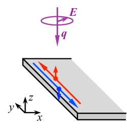
Consider a structure made of a 2D topological insulator with the edge along the axis, see Fig. 1. The structure supports a pair of counterpropagating edge modes with the opposite spin projections. It is excited by an electromagnetic wave with the electric field given by
| (1) |
where is the electric field amplitude and is the wave vector in the structure. The electromagnetic wave induces a dc electric current in the edge channel.
The dc current emerges in the second order in the electric field amplitude, i.e., linear in the radiation intensity, and is described by the phenomenological equation SturmanFridkin ; IvchenkoGanichev
| (2) |
where and are the third-rank and second-rank tensors, and the indices and run over the Cartesian coordinates , , and . The tensor describes the linear photogalvanic effect (LPGE), i.e., the photocurrent excited by linearly polarized ac electric field. The tensor stands for the circular photogalvanic effect (CPGE). This photocurrent is excited by elliptically or circularly polarized radiation and reverses its direction upon switching the sign of the photon helicity, since , where is the degree of circular polarization. Both LPGE and CPGE are possible in systems lacking the center of space inversion: LPGE is allowed in piezoelectric structures SturmanFridkin , while CPGE is allowed in gyrotropic structures IvchenkoGanichev , which follows from the symmetry of Eq. (2). Such a symmetry breaking naturally occurs at the edge of a 2D structure.
Elements of spatial symmetry present in the system may impose restrictions on the form of the and tensors. Generally, there are 5 types of semi-infinite quasi-two-dimensional crystalline structures. They are all illustrated in Fig. 2.
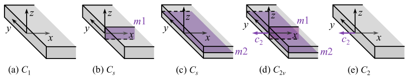
(i) A structure with an edge of the lowest possible symmetry is described by the point group which has no non-trivial symmetry elements, Fig. 2a. In such systems, all the components of the edge linear and circular photogalvanic tensors can be non-zero.
(ii) A semi-infinite structure with an edge can have the mirror plane perpendicular to the edge, in Fig. 2b. Such a system is described by the point group. This case is realized, e.g., in 2D topological insulators based on (001)-grown zinc-blende-type QWs with the edge along one of the crystallographic directions .
(iii) A structure can have the mirror plane lying in the center of the quasi-two-dimensional layer, in Fig. 2c. Such systems also belong to the point group but the mirror plane of the different orientation imposes different restrictions on the photogalvanic tensor components. Examples are (110)-grown QWs with symmetric confinement potential and any edge orientation except .
(iv) A structure can have both the and mirror planes, see Fig 2d. Then, it is described by the point group containing besides the two mirror planes the two-fold rotation axis . This is the highest possible symmetry of a semi-infinite 2D system. Such a symmetry is realized in symmetric (110)-grown QWs with the edge . In fact, this symmetry corresponds to commonly used isotropic models of 2D topological insulators, e.g., Bernevig-Hughes-Zhang (BHZ) model Bernevig2006 .
(v) Finally, a structure can possess the two-fold rotation axis but has neither nor mirror planes, Fig. 2e. Examples of such structures of the point group are symmetric (001)-grown QWs with the edge .
Non-zero components of the edge LPGE and CPGE tensors, and , respectively, for all the point groups listed above are summarized in Tab 1. The components describing the edge photocurrents at the normal incidence of radiation are in bold. It follows from the table that, in this geometry, the radiation induces both linear and circular photogalvanic currents.
| Point group | Examples in zinc-blende-type QWs | edge LPGE tensor | edge CPGE tensor |
|---|---|---|---|
| low-symmetry edges | all components | all components | |
| () | in asymmetric (001)-grown QWs | , | , |
| () | edges in symmetric (110)-grown QWs | , , , | |
| in symmetric (110)-grown QWs | |||
| in symmetric (001)-grown QWs | , | , |
In addition to the photogalvanic effects, which typically predominate in the photoresponse of non-centrosymmetric structures, a photocurrent may also originate from the joint action of the electric and magnetic fields of the radiation or from the modulation of the ac electric field in the real space. These effects belong to the class of photoelectric phenomena caused by light pressure (photon drag) Barlow1954 ; Perel1973 ; Shalygin2006 ; Karch2010 ; Obraztsov2014 ; Shalygin2016 . In structures of low spacial symmetry, the direction of the photon drag current is not necessarily locked to the photon wave vector . The electric current may even flow in the direction perpendicular to and have a pronounced polarization dependence Shalygin2006 ; Karch2010 ; Shalygin2016 . The edge photon drag effect is phenomenologically described by
| (3) |
where and are the tensors of the linear and circular photon drag effects. The results of a symmetry analysis of the photon drag effect for structures of different point groups are presented in Tab. 2. Interestingly, in structures lacking the horizontal mirror plane the edge current caused by the linear photon drag effect can emerge even at the normal incidence of radiation. The corresponding components of the tensor are in bold.
| Point group | Linear PDE tensor | Circular PDE tensor |
|---|---|---|
| all components | all components | |
| () | , , , , , , , | , , , , |
| () | , , , , , , , , , | , , , |
| , , , , , | , , | |
| , , , , , , , , , | , , , |
III Microscopic mechanisms of edge photocurrents
In this Section, we consider the mechanisms of photocurrent generation for different types of optical transitions involving topological edge states and present the results of microscopic calculations. We focus on 2D topological insulators based on zinc-blende-type QWs, such as commonly studied HgTe/CdHgTe QWs.
First, we briefly outline the electron structure of helical edge states in HgTe/CdHgTe QWs. These states are formed mainly from the electron-like and heavy-hole subbands Bernevig2006 . In the basis , , , and , the electron states in symmetric (001)-grown QW (D2d point group) are described by the effective 44 Hamiltonian Durnev2016
| (4) |
where is the in-plane electron wave vector, , , , ; , , , , and are the real-valued band-structure parameters.
The parameter describes the band gap and defines whether the system is in the trivial ( at ) or non-trivial ( at ) topological phase Bernevig2006 . The parameter describes the mixing of the and subbands at due to interface inversion asymmetry and bulk inversion asymmetry in the QW structure Tarasenko2015 ; Dai2008 ; Konig2008 ; Winkler2012 . Its experimental value is not well determined yet. Theoretical estimations for the HgTe/CdHgTe QWs of the close-to-critical thickness yield meV in the model Konig2008 ; Winkler2012 and meV in the atomistic (tight-binding and pseudopotential) approaches Tarasenko2015 ; Dai2008 .
The Hamiltonian (4) is written in the in-plane coordinate frame , , and , where , , and are the cubic axes, and is the angle describing the edge orientation. Below, we use the following set of the band-structure parameters: eVÅ, eVÅ2, eV Å2 Konig2008 , meV Tarasenko2015 , and meV, which corresponds to the topological gap of about meV.
The energy spectrum and wave functions of electron states in the topological insulator with the edge at are found from the Schrödinger equation
| (5) |
with a boundary condition for the wave function . We use the open boundary condition, i.e., at Durnev2016 ; Sonin2010 ; Scharf2012 ; Klipstein2015 . Boundary conditions of more general form were analyzed in Ref. Enaldiev2015 .
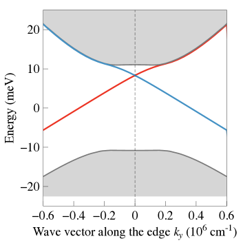
Figure 3 shows the energy spectrum of a topological-insulator structure calculated for the above parameters. The spectrum contains a pair of spin-polarized branches (shown by blue and red curves) which are in the band gap of the bulk QW states and correspond to the helical edge modes. The whole energy spectrum is asymmetric with respect to positive and negative energy due to electron-hole asymmetry introduced by the parameter in the Hamiltonian (4). In particular, the edge-state branches are shifted from the band gap center. At small wave vector along the edge , the edge states have linear dispersion and can be described by the effective Weyl Hamiltonian
| (6) |
where is the edge-state velocity and is the Pauli matrix in the pseudospin- space of the edge-state wave functions at , . At large , the dispersion of the edge states deviate from the linear law. The Hamiltonian (4) and the corresponding spectrum in Fig. 3 are obtained in the 4-subband model. This model does not take into account the complex structure of the valence band in the commonly studied 8-nm-wide HgTe/CdHgTe QWs. In fact, the valence band is strongly affected by the closely lying subband not included in the model, which leads to a nonmonotonic dispersion of the hole states with side maxima Raichev2012 ; Krishtopenko2018 ; Minkov2016 .
Now, we discuss the interaction of electromagnetic waves with the topological insulator and the origin of edge photocurrent generation. Depending on the photon energy and the position of the Fermi level in the structure, edge photocurrents are contributed by different types of optical transitions.
III.1 Direct optical transitions between spin branches
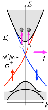
Direct optical transitions between the edge states with the pseudospin projections , see Fig. 4, take place when , where is the Fermi energy counted from the Weyl point Dora2012 ; Artemenko2013 ; Durnev2018 . If, additionally, the inequality is satisfied, where and are the energies of the conduction-band bottom and the valence-band top in the QW bulk, respectively, these are the only possible optical transitions in a pure structure.
Because of the selection rules to be discussed below, the optical transitions and induced by polarized radiation occur at different rates. This is illustrated in Fig. 4 by vertical arrows of different thicknesses. The asymmetry of the optical transitions results in an imbalance of electrons between the spin-momentum locked and branches giving rise to an electron spin polarization and a direct electric current. After an optical pulse, the spin polarization and the edge current decay with the characteristic time determined by spin-flip backscattering processes which are very rare. Under cw excitation, the decay is compensated by the optical generation of new spin-polarized electrons, and the photocurrent reaches its steady-state magnitude.
The optical transitions between the spin branches occur due to the interaction of edge carriers with the electric field Durnev2018 or magnetic field Dora2012 ; Artemenko2013 of the incident electromagnetic wave. The Hamiltonian of the electro-dipole electron-photon interaction has the form
| (7) |
where is the electric dipole operator. can be also rewritten in the equivalent form as , where is the electron charge, is the speed of light, is the velocity operator, and is the vector potential of the electromagnetic wave whose dependence on the coordinate is neglected. Microscopic theory based on the Hamiltonian (4) shows that the inter-branch matrix elements of is non-zero Durnev2018 . In the basis of the edge-state wave functions at , , the components of the electric dipole operator at small read
| (8) |
where and are the Pauli matrices, and and are real parameters. Both and vanish at since the time reversal symmetry does not allow a lifting of the Kramers degeneracy of the states and by an electric field.
We also note that the electro-dipole optical transitions are possible due to the lack of space inversion center in the QW structure and the parameters and scale with constant of the subband mixing in the Hamiltonian (4). Indeed, at zero the Hamiltonian (4) assumes the block-diagonal form and the edges states with stemming from these blocks are decoupled. Numeric calculations show that cm2 and cm2 for the band-structure parameters listed above Durnev2018 . Deriving analytical expressions for in terms of the band-structure parameters is a challenging task. In isotropic approximations, which corresponds to the effective point group for the QW structure with an edge, the components and vanish at any .
The Hamiltonian of the magneto-dipole interaction (the Zeeman Hamiltonian) in the basis of the wave functions has the form
| (9) |
where is the magnetic dipole operator, is the Bohr magneton, and are the -factor tensor components. The in-plane components are given by Durnev2016
| (10) |
where and are two independent -factors. The Zeeman gap in the edge-state spectrum opened by the out-of-plane magnetic field is theoretically studied in Ref. Durnev2016
With the account for both the electro-dipole and the magneto-dipole mechanisms of electron-photon interaction, the optical transitions induced by electromagnetic wave polarized in the QW plane are described by the matrix elements
| (11) |
where and are the matrix elements of the electric dipole and magnetic dipole operators, respectively, and are the amplitudes of the electric and magnetic fields of the radiation related by , is the refractive index of the medium, and is the unit vector along the radiation propagation direction . It follows from Eqs. (III.1) and (III.1) that, at small , the matrix elements are given by
| (12) | |||
The photocurrent originating from asymmetric corrections to the electron distribution function in the relaxation time approximation is given by Ganichev2003 ; Durnev2018
| (13) | |||||
where is the electron charge, is the relaxation time, and are the electron velocity and energy, respectively, and is the Fermi-Dirac distribution function. The time in Eq. (13) is the spin-flip scattering time of thermalized electrons at the Fermi level if electron thermalization within the edge channel, which is governed by electron-electron collisions and electron-phonon interaction, is faster than spin-flip scattering. In the opposite case, if electron thermalization is inefficient, is the spin-flip scattering time of hot carriers.
The optical orientation of edge electrons and the photocurrent sensitive to the photon helicity emerge in the electro-dipole approximation. The calculation of the photocurrent (13) with the matrix elements of the optical transitions determined by the electric dipole operator (III.1) yields Durnev2018
| (14) |
where is the radiation intensity, is the speed of light, is the absorption width of the edge channel for circularly polarized radiation calculated in the electro-dipole approximation,
| (15) |
and . Equation (14) describes the CPGE current which corresponds to the phenomenological parameter in Eq. (2) and Tab. 1.
For linearly polarized radiation, spin-dependent asymmetry in the optical transitions and the corresponding electric current emerge due to the interference of the electro-dipole and magneto-dipole transitions. This photocurrent has the form Durnev2018
| (16) |
where
| (17) |
and is the unit vector of the radiation polarization. The photocurrent (III.1) depends on the orientation of the edge with respect to the crystallographic axes and the radiation polarization plane with respect to the edge. It may also appear when the sample is excited by unpolarized radiation. The photocurrent (III.1) belongs to the class of linear photon drag effect, see first term in Eq. (3). For , which corresponds to the edge along and the point group of the structure, Eq. (III.1) shows that the linear PDE is described by the components and . For , which corresponds to the edge along and the point group of the structure, the linear PDE is described by the component . Both cases are in agreement with the symmetry analysis of the photon drag effect summarized in Tab. 2.
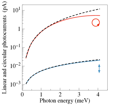
Figure 5 shows the magnitudes of the edge photocurrents originating from the circular photogalvanic effect and the linear photon drag effect in a HgTe/CdHgTe topological insulator as a function of the photon energy . The dependences are calculated for zero temperature, the Fermi level lying at the Weyl point, and the relaxation time ps estimated from the experiments on low-frequency edge conductivity Dantscher2017 . Solid curves present the results based on numerical calculations of the matrix elements of the electron-photon interaction at finite . Dashed curves show the low-energy analytical results plotted after Eqs. (14) and (III.1). For the radiation intensity 1 W/cm2, the photon energy meV, and the momentum relaxation time presented above, the photogalvanic and the photon drag currents at the normal incidence of radiation are in pA and fA ranges, respectively.
III.2 Edge-to-bulk optical transitions
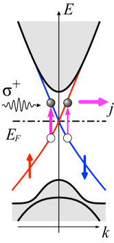
Another class of optical transitions, which can occur at edges of 2D topological insulators, are edge-to-bulk transitions leading to photoionization of the edge channel Dantscher2017 ; Artemenko2013 ; Kaladzhyan2015 ; Magarill2016 . These are the transitions between one-dimensional edge states and delocalized 2D states belonging to the conduction or the valence band, where is the 2D wave vector. The optical transitions from the edge channel to the conduction band take place if while the transitions from the valence band to the edge channel come into play at . The edge-to-band optical transitions induced by circularly polarized radiation and the corresponding mechanism of the generation of circular photocurrent in the edge channel are illustrated in Fig. 6.
Edge-to-bulk optical transitions are allowed in the electro-dipole approximation already in the isotropic BHZ model Kaladzhyan2015 . Therefore, they predominate if the photon energy is large enough to throw up electrons from the edge states to the conduction band (or from the valence band to the edge states above the Fermi level).
In the isotropic BHZ model, the optical transitions between the edge and conduction-band states occur with the pseudospin conservation. However, the rates of such transitions from the and states do not coincide with each other for circularly polarized radiation. This is similar to spin-dependent spin-conserving optical transitions between electron subbands in quantum wells Ganichev2003 . The difference in the photoionization rates is shown in Fig. 6 by vertical arrows of different thicknesses. Microscopically, the selection rules here are related to the fact that the edge states contain non-equal portions of the and states due to electron-hole asymmetry described by the parameter in the Hamiltonian (4).
The rates of the photoionization with the pseudospin conservation are given by the Fermi rule
| (18) |
where is the matrix element of the optical transitions from the edge states to the conduction-band states , is the energy of the conduction-band electrons, and is the wave vector of the conduction-band electrons in the direction normal to the edge.
The relative difference of the photoionization rates from the and states, and , respectively, is proportional to the helicity of incident photons and may be presented in the form
| (19) |
The dimensionless coefficient at is given by , Ref. Kaladzhyan2015 . Numerical calculations show that the coefficient has only weak dependence on and the photon energy Dantscher2017 .
To calculate the photocurrent originating from spin-selective photoionization of the edge channel we consider that the momentum relaxation time of bulk carriers is much shorter than that of edge carriers and neglect the photocurrent in the bulk states. We also assume that spin relaxation of bulk carriers is fast and photoionized electrons get unpolarized before they are trapped back on the helical edge states. In that case, the edge photocurrent is given by Dantscher2017
| (20) |
where is the absorption width of the edge channel for circularly polarized radiation.
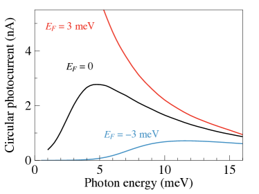
The excitation spectrum of the edge photocurrent for three different positions of the Fermi level is shown in Fig. 7. For the Fermi level lying inside the bulk gap, the photocurrent has a threshold dependence on . With the increase of the photocurrent rises, reaches its maximum, and then decreases. The decrease of the photocurrent at large is caused by the reduction of the photon density at a fixed radiation intensity and the reduction of the probability of the edge-to-band optical transitions. The latter stems from the weak overlap between the wave functions of edge and bulk states involved at large .
III.3 Indirect optical transitions in the edge channel
At small photon energy, when neither of the direct optical transitions considered above are possible, radiation can still be absorbed in an edge channel and leads to a photocurrent Entin2016 . In this case, the absorption of photons occurs as the result of indirect (Drude-like) optical transitions assisted by electron scattering from static defects or phonons to satisfy the energy and momentum conservation, Fig. 8. The photogalvanic effect for this type of transitions in quantum wells was considered in Ref. Tarasenko2007 .
Indirect optical transitions are theoretically treated as virtual processes via intermediate states, which can belong to the edge channel or the 2D conduction or valence subbands. The compound matrix element of the transitions with the initial and final states assisted by elastic scattering has the form
| (21) |
where the index runs over intermediate states, is the matrix element of electron-photon interaction, and is the matrix element of electron scattering.

There are two types of indirect optical transitions in edge channels: (a) transitions within the same spin branches, i.e., with in Eq. (21), and (b) inter-branch (spin-flip) transitions, i.e., with . They are sketched in Fig. 8a and Fig. 8b, respectively.
(a) For optical transitions with the pseudospin conservation, Fig. 8a, intermediate states lie either in the same edge branch or in the 2D conduction or valence subbands. The matrix element of the virtual transitions with intermediate states in the same branch is given by
| (22) |
Since the dispersion of the edge states is almost linear and the velocity has only weak dependence on , this contribution is small. The matrix element of the virtual transitions via conduction-band or valence-band 2D states can be estimated as
| (23) |
where is the matrix element of scattering. It is assumed here that the photon energy is much smaller than the energy separation between the Fermi level and 2D states which is of the order of the bulk band gap. Similarly to the direct edge-to-bulk transitions considered in Sec. III.2, the matrix elements and are not equal to each other for circularly polarized radiation. Such a spin-dependent asymmetry of the optical transitions leads to a circular photocurrent.
The circular photocurrent driven by the indirect optical transitions can be estimated as
| (24) |
where is the absorption width of the edge mode . The difference of the absorption widths and is proportional to and can be presented in the form
| (25) |
where is the total absorption width of the edge channel in this spectral range and is a dimensionless coefficient. This coefficient can be estimated as , where is defined by Eq. (19).
The absorption width for the indirect optical transitions can be estimated as
| (26) |
where is the momentum relaxation time of 2D carriers, is the square of the matrix element of scattering averaged over impurities.
Equations (24)-(26) provide the following estimation for the circular photocurrent caused by spin-conserving optical transitions in the edge channel
| (27) |
It shows that is about 10 pA for the radiation intensity W/cm2, the band gap meV, the photon energy meV, the relaxation time ps (extracted from the mobility of bulk carriers Dantscher2017 ), , and the relaxation time of edge carriers ps.
(b) For indirect optical transitions between the spin branches, Fig. 8b, the edge photocurrent can be presented in the form
| (28) |
where are the effective absorption widths for the spin-flip transitions.
The indirect transitions with spin flip can also occur via intermediate states in the conduction or valence subbands of the QW. The difference of the absorption widths for this kind of processes can be estimated as
| (29) |
where and are the matrix elements of inter-subband and intra-subband scattering, respectively, and is the absorption width given by Eq. (26). The photocurrent caused by spin-flip indirect optical transitions (28) is order of magnitude smaller than the photocurrent caused by spin-conserving optical transitions (27).
III.4 Experimental results
Edge photocurrents in 2D topological insulators were observed in Ref. Dantscher2017 . The experiments were carried out on Hg0.3Cd0.7Te/HgTe/Hg0.3Cd0.7Te QW structures with the well width of 8 nm grown by molecular beam epitaxy on GaAs substrates. The photocurrent was excited by circularly polarized terahertz radiation with the photon energy smaller than the QW band gap. It was observed that photocurrents on the opposite edges of the samples flowed consistently in the opposite directions. The direction of the edge photocurrent was determined by the sign of photon helicity, i.e., the photocurrent was reversed by switching the radiation polarization from to . The samples were equipped with semitransparent top gates which enabled the tuning of the Fermi level.
It was observed that the edge photocurrent is efficiently generated when the Fermi level is in the band gap and has a maximum at the Fermi level lying somewhat below the conduction-band bottom Dantscher2017 . Analysis of the dependence of the edge photocurrent on the gate voltage and the efficiency of different mechanisms of current generation revealed that the photocurrent in this range of is dominated by photoionization of the edge states into the conduction band. The performed microscopic calculations supported this scenario. At negative where the Fermi level is shifted towards the valence band, the photocurrent changes its sign and exhibits another rise. This rise may be related to optical transitions from the valence band to the edge states. The change of the photocurrent sign, however, is unclear and odds with the BHZ model which suggests the same current direction for the edge-to-conduction-band and valence-band-to-edge transitions Dantscher2017 ; Magarill2016 . It may be related to the complex structure of the valence band in 8-nm-wide HgTe QWs not included in the BHZ model. Another explanation could be that the photocurrent in this range of is related to indirect optical transitions within the edge channel which are manifested due to strong energy dependence of the relaxation time or nonlinearity of the edge-state dispersion.
The study of QW-based topological insulators with higher quality and larger band gap, which are already available Leubner2016 , will enable the observation of edge photocurrents related to different types of optical transitions and provide valuable information about the properties of helical states.
To summarize, we have discussed the high-frequency and optical properties of helical edge channels in two-dimensional topological insulators based on zinc-blende-type quantum wells. The interaction of electrons in the edge channel with a polarized electromagnetic wave is spin dependent and asymmetric in the momentum space, which results in edge photocurrents sensitive to the photon helicity. Depending on the radiation frequency and the position of the Fermi level in the structure, the edge photocurrents are contributed by different types of optical transitions. The most probable optical transitions involving edge states are direct transitions between the edge states and the bulk states in the quantum well. They are allowed already in centrosymmetric models on topological insulators and determine the edge photocurrent if the photon energy is large enough to throw up edge electrons (or holes) to the bulk conduction-band (or valence-band) states. Optical transitions within the edge channel come into play for smaller photon energies. There can be direct transitions between the “spin-up” and “spin-down” edge states and indirect transitions assisted by electron scattering from static defects or phonons. The former occur in the electro-dipole approximation due to the lack of space inversion center in the quantum well while the latter require electron scattering. The relative strength of the photocurrents contributed by these direct and indirect transitions depends on the quality and the band-structure parameters of the topological insulator.
The work was supported by the Russian Science Foundation (project 17-12-01265).
References
- (1) M. Z. Hasan and C. L. Kane, Colloquium: Topological insulators, Rev. Mod. Phys. 82, 3045 (2010).
- (2) X.-L. Qi and S.-C. Zhang. Topological insulators and superconductors, Rev. Mod. Phys. 83, 1057 (2011).
- (3) J. E. Moore, The birth of topological insulators, Nature 464, 194 (2010).
- (4) B. A. Volkov and O. A. Pankratov, Inverted contact in semiconductors – a new inhomogeneous structure with a two-dimensional gas of zero-mass electrons, Sov. Phys. Uspekhi 29, 579 (1986).
- (5) B. A. Volkov and O. A. Pankratov, Two-dimensional massless electrons in an inverted contact, JETP Lett. 42, 178 (1985).
- (6) O. A. Pankratov, S. V. Pakhomov, and B. A. Volkov, Supersymmetry in heterojunctions: Band-inverting contact on the basis of Pb1-xSnxTe and Hg1-xCdxTe, Solid State Commun. 61, 93 (1987).
- (7) B. A. Bernevig and S.-C. Zhang, Quantum spin Hall effect, Phys. Rev. Lett. 96, 106802 (2006).
- (8) C. L. Kane and E. J. Mele, topological order and the quantum spin Hall effect, Phys. Rev. Lett. 95, 146802 (2005).
- (9) L. Fu, C. L. Kane, and E. J. Mele. Topological insulators in three dimensions, Phys. Rev. Lett. 98, 106803 (2007).
- (10) Y. Ando, Topological insulator materials, J. Phys. Soc. Japan 82, 102001 (2013).
- (11) H. Zhang, C.-X. Liu, X.-L. Qi, X. Dai, Z. Fang, and S.-C. Zhang, Topological insulators in Bi2Se3, Bi2Te3 and Sb2Te3 with a single Dirac cone on the surface, Nat. Phys. 5, 438 (2009).
- (12) Y. Xia, D. Qian, D. Hsieh, L. Wray, A. Pal, H. Lin, A. Bansil, D. Grauer, Y. S. Hor, R. J. Cava, and M. Z. Hasan, Observation of a large-gap topological-insulator class with a single Dirac cone on the surface, Nat. Phys. 5, 398 (2009).
- (13) L. Fu and C. L. Kane, Topological insulators with inversion symmetry, Phys. Rev. B 76, 045302 (2007).
- (14) C. Brüne, C. X. Liu, E. G. Novik, E. M. Hankiewicz, H. Buhmann, Y. L. Chen, X. L. Qi, Z. X. Shen, S.-C. Zhang, and L. W. Molenkamp, Quantum Hall effect from the topological surface states of strained bulk HgTe, Phys. Rev. Lett. 106, 126803 (2011).
- (15) D. A. Kozlov, Z. D. Kvon, E. B. Olshanetsky, N. N. Mikhailov, S. A. Dvoretsky, and D. Weiss, Transport properties of a 3D topological insulator based on a strained high-mobility HgTe film, Phys. Rev. Lett. 112, 196801 (2014).
- (16) B. A. Bernevig, T. L. Hughes, and S.-C. Zhang, Quantum spin hall effect and topological phase transition in HgTe quantum wells, Science 314, 1757 (2006).
- (17) M. König, S. Wiedmann, C. Brüne, A. Roth, H. Buhmann, L. W. Molenkamp, X.-L. Qi, and S.-C. Zhang, Quantum spin Hall insulator state in HgTe quantum wells, Science 318, 766 (2007).
- (18) C. Liu, T. L. Hughes, X.-L. Qi, K. Wang, and S.-C. Zhang, Quantum spin Hall effect in inverted type-II semiconductors, Phys. Rev. Lett. 100, 236601 (2008).
- (19) S. S. Krishtopenko, S. Ruffenach, F. Gonzalez-Posada, G. Boissier, M. Marcinkiewicz, M. A. Fadeev, A. M. Kadykov, V. V. Rumyantsev, S. V. Morozov, V. I. Gavrilenko, C. Consejo, W. Desrat, B. Jouault, W. Knap, E. Tournie, and F. Teppe, Temperature-dependent terahertz spectroscopy of inverted-band three-layer InAs/GaSb/InAs quantum well, Phys. Rev. B 97, 245419 (2018).
- (20) X. Qian, J. Liu, L. Fu, and J. Li, Quantum spin Hall effect in two-dimensional transition metal dichalcogenides, Science 20, 1256815 (2014).
- (21) Z. Fei, T. Palomaki, S. Wu, W. Zhao, X. Cai, B. Sun, P. Nguyen, J. Finney, X. Xu, and D. H. Cobden, Edge conduction in monolayer WTe2, Nat. Phys. 13, 677 (2017).
- (22) D. Hsieh, Y. Xia, D. Qian, L. Wray, J. H. Dil, F. Meier, J. Osterwalder, L. Patthey, J. G. Checkelsky, N. P. Ong, A. V. Fedorov, H. Lin, A. Bansil, D. Grauer, Y. S. Hor, R. J. Cava, and M. Z. Hasan, A tunable topological insulator in the spin helical Dirac transport regime, Nature 460, 1101 (2009).
- (23) J. G. Checkelsky, Y. S. Hor, M.-H. Liu, D.-X. Qu, R. J. Cava, and N. P. Ong, Quantum interference in macroscopic crystals of nonmetallic Bi2Se3, Phys. Rev. Lett. 103, 246601 (2009).
- (24) J. G. Analytis, J.-H. Chu, Y. Chen. F. Corredor, R. D. McDonald, Z. X. Shen, and I. R. Fisher, Bulk Fermi surface coexistence with Dirac surface state in Bi2Se3: A comparison of photoemission and Shubnikov-de-Haas measurements, Phys. Rev. B 81, 205407 (2010).
- (25) Z. Ren, A. A. Taskin, S. Sasaki, K. Segawa, and Y. Ando, Optimizing Bi2-xSbxTe3-ySe solid solutions to approach the intrinsic topological insulator regime, Phys. Rev. B 84, 165311 (2011).
- (26) B. Xia, P. Ren, A. Sulaev, P. Liu, S.-Q. Shen, and L. Wang, Indications of surface-dominated transport in single crystalline nanoflake devices of topological insulator Bi1.5Sb0.5Te1.8Se1.2, Phys. Rev. B 87, 085442 (2013).
- (27) Y. Pan, D. Wu, J. R. Angevaare, H. Luigjes, E. Frantzeskakis, N. de Jong, E. van Heumen, T. V. Bay, B. Zwartsenberg, and Y. K. Huang, Low carrier concentration crystals of the topological insulator Bi2-xSbxTe3-ySey: A magnetotransport study, New J. Phys. 16, 123035 (2014).
- (28) A. M. Shuvaev, G. V. Astakhov, G. Tkachov, C. Brüne, H. Buhmann, L. W. Molenkamp, and A. Pimenov, Terahertz quantum Hall effect of Dirac fermions in a topological insulator, Phys. Rev. B 87, 121104(R) (2013).
- (29) V. Dziom, A. Shuvaev, A. Pimenov, G. V. Astakhov, C. Ames, K. Bendias, J. Böttcher, G. Tkachov, E. M. Hankiewicz, C. Brüne, H. Buhmann, and L. W. Molenkamp, Observation of the universal magnetoelectric effect in a 3D topological insulator, Nat. Comm. 8, 15197 (2017).
- (30) A. Roth, C. Brüne, H. Buhmann, L. W. Molenkamp, J. Maciejko, X.-L. Qi, and S.-C. Zhang, Nonlocal transport in the quantum spin Hall state, Science 325, 294 (2009).
- (31) G. M. Gusev, Z. D. Kvon, O. A. Shegai, N. N. Mikhailov, S. A. Dvoretsky, and J. C. Portal, Transport in disordered two-dimensional topological insulators, Phys. Rev. B 84, 121302(R) (2011).
- (32) S. Hart, H. Ren, T. Wagner, P. Leubner, M. Mühlbauer, C. Brüne, H. Buhmann, L. W. Molenkamp, and A. Yacoby, Induced superconductivity in the quantum spin Hall edge, Nat. Phys. 10, 638 (2014).
- (33) E. Y. Ma, M. R. Calvo, J. Wang, B. Lian, M. Mühlbauer, C. Brüne, Y.-T. Cui, K. Lai, W. Kundhikanjana, Y. Yang, M. Baenninger, M. König, C. Ames, H. Buhmann, P. Leubner, L. W. Molenkamp, S.-C. Zhang, D. Goldhaber-Gordon, M. A. Kelly, and Z.-X. Shen, Unexpected edge conduction in mercury telluride quantum wells under broken time-reversal symmetry, Nat. Comm. 6, 7252 (2015).
- (34) E. S. Tikhonov, D. V. Shovkun, V. S. Khrapai, Z. D. Kvon, N. N. Mikhailov, and S. A. Dvoretsky, Shot noise of the edge transport in the inverted band HgTe quantum wells, JETP Lett. 101, 708 (2015).
- (35) A. Kononov, S. V. Egorov, Z. D. Kvon, N. N. Mikhailov, S. A. Dvoretsky, and E. V. Deviatov, Evidence on the macroscopic length scale spin coherence for the edge currents in a narrow HgTe quantum well, JETP Lett. 101, 814 (2015).
- (36) A. M. Kadykov, S. S. Krishtopenko, B. Jouault, W. Desrat, W. Knap, S. Ruffenach, C. Consejo, J. Torres, S. V. Morozov, N. N. Mikhailov, S. A. Dvoretskii, and F. Teppe, Temperature-induced topological phase transition in HgTe quantum wells, Phys. Rev. Lett. 120, 086401 (2018).
- (37) L. I. Maragill and M. V. Entin, Photogalvanic effect in films, Sov. Phys. Solid State 21, 743 (1979).
- (38) V. L. Alperovich, V. I. Belinicher, V. N. Novikov, and A. S. Terekhov, Photogalvanic effects investigation in gallium arsenide, Ferroelectrics 45, 1 (1982).
- (39) C. B. Schmidt, S. Priyadarshi, S. A. Tarasenko, and M. Bieler, Ultrafast magneto-photocurrents in GaAs: Separation of surface and bulk contributions, Appl. Phys. Lett. 106, 142108 (2015).
- (40) J. Karch, C. Drexler, P. Olbrich, M. Fehrenbacger, M. Hirmer, M. M. Glazov, S. A. Tarasenko, E. L. Ivchenko, B. Birkner, J. Eroms, D. Weiss, R. Yakimova, S. Lara-Avila, S. Kubatkin, M. Ostler, T. Seyller, and S. D. Ganichev, Terahertz radiation driven chiral edge currents in graphene, Phys. Rev. Lett. 107, 276601 (2011).
- (41) P. Reimann, Brownian motors: noisy transport far from equilibrium, Phys. Rep. 361, 57 (2002).
- (42) V. I. Fal’ko, Rectifying properties of 2D inversion layers in a parallel magnetic field, Sov. Phys. Solid State 31, 561 (1989).
- (43) S. A. Tarasenko, Direct current driven by ac electric field in quantum wells, Phys. Rev. B 83, 035313 (2011).
- (44) C. Drexler, S. A. Tarasenko, P. Olbrich, J. Karch, M. Hirmer, F. Müller, M. Gmitra, J. Fabian, R. Yakimova, S. Lara-Avila, S. Kubatkin, M. Wang, R. Vajtai, P. M. Ajayan, J. Kono, and S. D. Ganichev, Magnetic quantum ratchet effect in graphene, Nat. Nanotechnol. 8, 104 (2013).
- (45) B. I. Sturman and V. M. Fridkin, The Photovoltaic and Photorefractive Effects in Non-Centrosymmetric Materials (Gordon and Breach, New York, 1992).
- (46) E. L. Ivchenko and S. D. Ganichev, Spin Photogalvanics in Spin Physics in Semiconductors, edited by M. I. Dyakonov (Springer, Berlin, 2008).
- (47) A.M. Glass, D. von der Linde, T.J. Negran, Appl. Phys. Lett. (1974).
- (48) V. M. Asnin, A. A. Bakun, A.M. Danishevskii, E.L. Ivchenko, G.E. Pikus, A.A. Rogachev, Observation of a photo-emf that depends on the sign of the circular polarization of the light, JETP Lett. 28, 74 (1978).
- (49) S. D. Ganichev, V. V. Bel’kov, P. Schneider, E. L. Ivchenko, S. A. Tarasenko, W. Wegscheider, D. Weiss, D. Schuh, E. V. Beregulin, and W. Prettl, Resonant inversion of the circular photogalvanic effect in -doped quantum wells, Phys. Rev. B 68, 035319 (2003).
- (50) M. Bieler, N. Laman, H. M. van Driel, and A. L. Smirl, Ultrafast spin-polarized electrical currents injected in a strained zinc blende semiconductor by single color pulses, Appl. Phys. Lett. 86, 061102 (2005).
- (51) C. L. Yang, H. T. He, Lu Ding, L. J. Cui, Y. P. Zeng, J. N. Wang, and W. K. Ge, Spectral dependence of spin photocurrent and current-induced spin polarization in an InGaAs/InAlAs two-dimensional electron gas, Phys. Rev. Lett. 96, 186605 (2006).
- (52) P. Olbrich, J. Allerdings, V. V. Bel’kov, S. A. Tarasenko, D. Schuh, W. Wegscheider, T. Korn, C. Schüller, D. Weiss, and S. D. Ganichev, Magnetogyrotropic photogalvanic effect and spin dephasing in (110)-grown GaAs/AlGaAs quantum well structures, Phys. Rev. B 79, 245329 (2009).
- (53) S. Priyadarshi, K. Pierz, and M. Bieler, All-optically induced ultrafast photocurrents: Beyond the instantaneous coherent response, Phys. Rev. Lett. 109, 216601 (2012).
- (54) P. Olbrich, C. Zoth, P. Vierling, K.-M. Dantscher, G. V. Budkin, S. A. Tarasenko, V. V. Bel’kov, D. A. Kozlov, Z. D. Kvon, N. N. Mikhailov, S. A. Dvoretsky, and S. D. Ganichev, Giant photocurrents in a Dirac fermion system at cyclotron resonance, Phys. Rev. B 87, 235439 (2013).
- (55) S. D. Ganichev and L. E. Golub, Interplay of Rashba/Dresselhaus spin splittings probed by photogalvanic spectroscopy – A review, Phys. Status Solidi B 251, 1801 (2014).
- (56) J. Li, W. Yang, J.-T. Liu, W. Huang, C. Li, and S.-Y. Chen, Enhanced circular photogalvanic effect in HgTe quantum wells in the heavily inverted regime, Phys. Rev. B 95, 035308 (2017).
- (57) G. M. Mikheev, A. S. Saushin, V. M. Styapshin, and Yu. P. Svirko, Interplay of the photon drag and the surface photogalvanic effects in the metal-semiconductor nanocomposite, Sci. Rep. 8, 8644 (2018).
- (58) R. D. R. Bhat, F. Nastos, N. Ali, and J. E. Sipe, Pure spin current from one-photon absorption of linearly polarized light in noncentrosymmetric semiconductors, Phys. Rev. Lett. 94, 96603 (2005).
- (59) S.A. Tarasenko and E.L. Ivchenko, Pure spin photocurrents in low-dimensional structures, JETP Lett. 81, 231 (2005).
- (60) H. Zhao, X. Pan, A. L. Smirl, R. D. R. Bhat, A. Najmaie, J. E. Sipe, and H. M. van Driel, Injection of ballistic pure spin currents in semiconductors by a single-color linearly polarized beam, Phys. Rev. B 72, 201302 (2005).
- (61) S. D. Ganichev, V. V. Bel’kov, S. A. Tarasenko, S. N. Danilov, S. Giglberger, Ch. Hoffmann, E. L. Ivchenko, D. Weiss, W. Wegscheider, C. Gerl, D. Schuh, J. Stahl, J. De Boeck, G. Borghs, and W. Prettl, Zero-bias spin separation, Nat. Phys. 2, 609 (2006).
- (62) S. D. Ganichev, S. A. Tarasenko, V. V. Bel’kov, P. Olbrich, W. Eder, D.R. Yakovlev, V. Kolkovsky, W. Zaleszczyk, G. Karczewski, T. Wojtowicz, and D. Weiss, Spin currents in diluted magnetic semiconductors, Phys. Rev. Lett. 102, 156602 (2009).
- (63) J. Karch, S. A. Tarasenko, E. L. Ivchenko, J. Kamann, P. Olbrich, M. Utz, Z. D. Kvon, S. D. Ganichev, Photoexcitation of valley-orbit currents in (111)-oriented silicon metal-oxide-semiconductor field-effect transistors, Phys. Rev. B 83, 121312(R) (2011).
- (64) L. E. Golub, S. A. Tarasenko, M. V. Entin, and L. I. Magarill, Valley separation in graphene by polarized light, Phys. Rev. B 84, 195408 (2011).
- (65) R. R. Hartmann and M. E. Portnoi, Optoelectronic Properties of Carbon-based Nanostructures: Steering electrons in graphene by electromagnetic fields (LAP LAMBERT Academic Publishing, Saarbrucken, 2011).
- (66) H. Yuan, X. Wang, B. Lian, H. Zhang, X. Fang, B. Shen, G. Xu, Y. Xu, Sh.-Ch. Zhang, H. Y. Hwang, and Y. Cui, Generation and electric control of spin-valley-coupled circular photogalvanic current in WSe2, Nat. Nanotechnol. 9, 851 (2014).
- (67) T. L. Linnik, Photoinduced valley currents in strained graphene, Phys. Rev. B 90, 075406 (2014).
- (68) Y. B. Lyanda-Geller, S. Li, and A. V. Andreev, Polarization-dependent photocurrents in polar stacks of van der Waals solids, Phys. Rev. B 92, 241406(R) (2015).
- (69) D. Hsieh, J. W. McIver, D. H. Torchinsky, D. R. Gardner, Y. S. Lee, and N. Gedik, Nonlinear optical probe of tunable surface electrons on a topological insulator, Phys. Rev. Lett. 106, 057401 (2011).
- (70) J. W. McIver, D. Hsieh, H. Steinberg, P. Jarillo-Herrero, and N. Gedik, Control over topological insulator photocurrents with light polarization, Nat. Nanotech. 7, 96 (2012).
- (71) P. Olbrich, L. E. Golub, T. Herrmann, S. N. Danilov, H. Plank, V. V. Bel’kov, G. Mussler, Ch. Weyrich, C. M. Schneider, J. Kampmeier, D. Grützmacher, L. Plucinski, M. Eschbach, and S. D. Ganichev, Room-temperature high-frequency transport of Dirac fermions in epitaxially grown Sb2Te3- and Bi2Te3-based topological insulators, Phys. Rev. Lett. 113, 096601 (2014).
- (72) K.-M. Dantscher, D. A. Kozlov, P. Olbrich, C. Zoth, P. Faltermeier, M. Lindner, G. V. Budkin, S. A. Tarasenko, V. V. Bel’kov, Z. D. Kvon, N. N. Mikhailov, S. A. Dvoretsky, D. Weiss, B. Jenichen, and S. D. Ganichev, Cyclotron-resonance-assisted photocurrents in surface states of a three-dimensional topological insulator based on a strained high-mobility HgTe film, Phys. Rev. B 92, 165314 (2015).
- (73) A. M. Shikin, I. Klimovskikh, M. V. Filyanina, A. A. Rybkina, D. A. Pudikov, K. A. Kokh, and O. E. Tereshchenko, Surface spin-polarized currents generated in topological insulators by circularly polarized synchrotron radiation and their photoelectron spectroscopy indication, Phys. Solid State 58, 1675 (2016).
- (74) S. Y. Hamh, S.-H. Park, S.-K. Jerng, J. H. Jeon, S.-H. Chun, and J. S. Lee, Helicity-dependent photocurrent in a Bi2Se3 thin film probed by terahertz emission spectroscopy, Phys. Rev. B 94, 161405(R) (2016).
- (75) A. V. Galeeva, S. G. Egorova, V. I. Chernichkin, M. E. Tamm, L. V. Yashina, V. V. Rumyantsev, S. V. Morozov, H. Plank, S. N. Danilov, L. I. Ryabova, and D. R. Khokhlov, Manifestation of topological surface electron states in the photoelectromagnetic effect induced by terahertz laser radiation, Semicond. Sci. Technol. 31, 095010 (2016).
- (76) Y. Pan, Q.-Z. Wang, A. L. Yeats, T. Pillsbury, T. C. Flanagan, A. Richardella, H. Zhang, D. D. Awschalom, C.-X. Liu, and N. Samarth, Helicity dependent photocurrent in electrically gated (Bi1-xSbx)2Te3 thin films, Nat. Comm. 8, 1037 (2017).
- (77) Y. Q. Huang, Y. X. Song, S. M. Wang, I. A. Buyanova, and W. M. Chen, Spin injection and helicity control of surface spin photocurrent in a three dimensional topological insulator, Nat. Comm. 8, 15401 (2017).
- (78) K. Kuroda, J. Reimann, K. A. Kokh, O. E. Tereshchenko, A. Kimura, J. Güdde, and U. Höfer, Ultrafast energy- and momentum-resolved surface Dirac photocurrents in the topological insulator Sb2Te3, Phys. Rev. B 95, 081103(R) (2017).
- (79) K.-M. Dantscher, D. A. Kozlov, M. T. Scherr, S. Gebert, J. Bärenfänger, M. V. Durnev, S. A. Tarasenko, V. V. Bel’kov, N. N. Mikhailov, S. A. Dvoretsky, Z. D. Kvon, J. Ziegler, D. Weiss, and S. D. Ganichev, Photogalvanic probing of helical edge channels in two-dimensional HgTe topological insulators, Phys. Rev. B 95, 201103(R) (2017).
- (80) H. Plank and S.D. Ganichev, A review on terahertz photogalvanic spectroscopy of Bi2Te3- and Sb2Te3-based three dimensional topological insulators, Solid-State Electronics 147, 44 (2018).
- (81) H. M. Barlow, Application of the Hall effect in a semiconductor to the measurement of power in an electromagnetic field, Nature (London) 173, 41 (1954).
- (82) V. I. Perel’ and Ya. M. Pinskii, Constant current in conducting media due to a high-frequency electromagnetic field, Sov. Phys. Solid State 15, 688 (1973).
- (83) V. A. Shalygin, H. Diehl, Ch. Hoffmann, S. N. Danilov, T. Herrle, S. A. Tarasenko, D. Schuh, Ch. Gerl, W. Wegscheider, W. Prettl, and S. D. Ganichev, Spin photocurrents and circular photon drag effect in (110)-grown quantum well structures, JETP Lett. 84, 570 (2006).
- (84) J. Karch, J. Karch, P. Olbrich, M. Schmalzbauer, C. Zoth, C. Brinsteiner, M. Fehrenbacher, U. Wurstbauer, M. M. Glazov, S. A. Tarasenko, E. L. Ivchenko, D. Weiss, J. Eroms, R. Yakimova, S. Lara-Avila, S. Kubatkin, and S. D. Ganichev, Dynamic Hall effect driven by circularly polarized light in a graphene layer, Phys. Rev. Lett. 105, 227402 (2010).
- (85) P. A. Obraztsov, N. Kanda, K. Konishi, M. Kuwata-Gonokami, S. V. Garnov, A. N. Obraztsov, and Yu. P. Svirko, Photon-drag-induced terahertz emission from graphene, Phys. Rev. B 90, 241416 (2014).
- (86) V. A. Shalygin, M. D. Moldavskaya, S. N. Danilov, I. I. Farbshtein, L. E. Golub, Circular photon drag effect in bulk tellurium, Phys. Rev. B 93, 045207 (2016).
- (87) M. V. Durnev and S. A. Tarasenko, Magnetic field effects on edge and bulk states in topological insulators based on HgTe/CdHgTe quantum wells with strong natural interface inversion asymmetry, Phys. Rev. B 93, 075434 (2016).
- (88) S. A. Tarasenko, M. V. Durnev, M. O. Nestoklon, E. L. Ivchenko, J.-W. Luo, and A. Zunger, Split Dirac cones in HgTe/CdTe quantum wells due to symmetry-enforced level anticrossing at interfaces, Phys. Rev. B 91, 081302 (2015).
- (89) X. Dai, T. L. Hughes, X.-L. Qi, Z. Fang, and S.-C. Zhang, Helical edge and surface states in HgTe quantum wells and bulk insulators, Phys. Rev. B 77, 125319 (2008).
- (90) M. König, H. Buhmann, L. W. Molenkamp, T. Hughes, C.-X. Liu, X.-L. Qi, and S.-C. Zhang, The quantum spin Hall effect: Theory and experiment, J. Phys. Soc. Jpn. 77, 031007 (2008).
- (91) R. Winkler, L. Y. Wang, Y. H. Lin, and C. S. Chu, Robust level coincidences in the subband structure of quasi-2D systems, Solid State Commun. 152, 2096 (2012).
- (92) E. B. Sonin, Edge accumulation and currents of moment in two-dimensional topological insulators, Phys. Rev. B 82, 113307 (2010).
- (93) B. Scharf, A. Matos-Abiague, and J. Fabian, Magnetic properties of HgTe quantum wells, Phys. Rev. B 86, 075418 (2012).
- (94) P. C. Klipstein, Structure of the quantum spin Hall states in HgTe/CdTe and InAs/GaSb/AlSb quantum wells, Phys. Rev. B 91, 035310 (2015).
- (95) V. V. Enaldiev, I. V. Zagorodnev, and V. A. Volkov, Boundary conditions and surface state spectra in topological insulators, JETP Lett. 101, 89 (2015).
- (96) O. E. Raichev, Effective Hamiltonian, energy spectrum, and phase transition induced by in-plane magnetic field in symmetric HgTe quantum wells, Phys. Rev. B 85, 045310 (2012).
- (97) S. S. Krishtopenko and F. Teppe, Realistic picture of helical edge states in HgTe quantum wells, Phys. Rev. B 97, 165408 (2018).
- (98) G. M. Minkov, A.V. Germanenko, O. E. Rut, A. A. Sherstobitov, M. O. Nestoklon, S. A. Dvoretski, and N. N. Mikhailov, Spin-orbit splitting of valence and conduction bands in HgTe quantum wells near the Dirac point, Phys. Rev. B 93, 155304 (2016).
- (99) B. Dóra, J. Cayssol, F. Simon, and R. Moessner, Optically engineering the topological properties of a spin Hall insulator, Phys. Rev. Lett. 108, 056602 (2012).
- (100) S. N. Artemenko and V. O. Kaladzhyan, Photogalvanic effects in topological insulators, JETP Letters 97, 82 (2013).
- (101) M. V. Durnev and S. A. Tarasenko, Optical properties of helical edge channels in zinc-blende-type topological insulators: Selection rules, circular and linear dichroism, circular and linear photocurrents, Journ. of Phys.: Cond. Matt. 31, 035301 (2019).
- (102) V. Kaladzhyan, P. P. Aseev, and S. N. Artemenko, Photogalvanic effect in the HgTe/CdTe topological insulator due to edge-bulk optical transitions, Phys. Rev. B 92, 155424 (2015).
- (103) L. I. Magarill and M. V. Entin, Circular photogalvanic effect caused by the transitions between edge and 2D states in a 2D topological insulator, JETP Lett. 104, 771 (2016).
- (104) M. V. Entin and L. I. Magarill, Edge absorption and circular photogalvanic effect in 2D topological insulator edges, JETP Lett. 103, 711 (2016).
- (105) S. A. Tarasenko, Orbital mechanism of the circular photogalvanic effect in quantum wells, JETP Lett. 85, 182 (2007).
- (106) P. Leubner, L. Lunczer, C. Brüne, H. Buhmann, and L. W. Molenkamp, Strain engineering of the band gap of HgTe quantum wells using superlattice virtual substrates, Phys. Rev. Lett. 117, 086403 (2016).