Surface Impedance Measurements on Nb3Sn in High Magnetic Fields
Abstract
Nb3Sn is a superconductor of great relevance for perspective RF applications. We present for the first time surface impedance () measurements at 15 GHz and low RF field amplitude on Nb3Sn in high magnetic fields up to 12 T, with the aim of increasing the knowledge of Nb3Sn behavior in such conditions. is a fundamental material parameter that directly gives useful information about the dissipative and reactive phenomena when the superconductor is subjected to high-frequency excitations. Therefore, we present an analysis of the measured with the aim of extracting interesting data about pinning in Nb3Sn at high frequencies. From we extract the vortex motion complex resistivity to obtain the -parameter and the depinning frequency in high magnetic fields. The comparison of the results with the literature shows that the measured on bulk Nb3Sn is several times greater than that of pure Nb. This demonstrates how Nb3Sn can be a good candidate for RF technological applications, also in high magnetic fields.
Index Terms:
High magnetic fields, microwave, Nb3Sn, depinning frequency, surface impedance.I Introduction
Currently Nb3Sn is the most interesting technological superconductor both for high performance dc applications like magnets for nuclear fusion or particle accelerators, and for potential radiofrequency applications as resonating cavities [1, 2, 3, 4, 5, 6].
In applications like superconductive power cables in high magnetic fields, it is well known that vortex motion is the main contribution to the conduction losses. Hence, the experimental study of fluxons behavior, and their pinning, is of great relevance.
At radiofrequency (RF) and microwaves (mw), pinning is still a relevant topic, since vortices are much more free to dissipate. Challenging applications of Nb3Sn are represented by the RF accelerating cavities for particles accelerators [3, 7]. Nb cavities are currently being used but their technological limits seem to be reached [3], so to overcome their performances it is necessary to consider other superconductors and Nb3Sn is a potential candidate [8]. Nb3Sn offers approximately twice the critical temperature and the superheating field with respect to Nb. This yields an improved cryogenic efficiency and perspective higher accelerating fields [3]. However, it must be mentioned that to date, Nb3Sn cavities show a limit of peak surface magnetic field at mT [3] which is still lower than the highest peak RF magnetic field reached with bulk Nb cavities mT [9].
The improvement of the actual technological limits of this superconductor, in terms of critical current and superheating field , is a mandatory requirement for the development of some of the presented applications. For this reason an in depth study of the RF electrodynamic response of Nb3Sn when subjected to extreme working conditions is needed.
For RF applications the depinning frequency is the most relevant parameter because it marks the boundary between the frequency band where the response of fluxons to harmonic excitation is mainly elastic () and the range where the vortex oscillation becomes purely dissipative () [10]. The higher the the higher the usable working frequencies are with a given SC with reduced dissipation.
Despite the relevance of Nb3Sn, to our knowledge no high magnetic fields microwave measurements are present in literature on Nb3Sn. In this work we present the first microwave characterization of Nb3Sn in high magnetic fields through measurements, performed with low RF field amplitude. From the analysis, the is determined as a function of temperature . We find that attains values much larger than in Nb, thus making Nb3Sn an attractive material for its RF and mw potential performance in high magnetic fields.
The paper is organized as follows. In Sec.II we briefly recall the main model for in a superconductor in the vortex state. In Sec.III we describe the experimental setup and method. In Sec.IV we present the characterization of the sample and the experimental results for . Short conclusions are presented in Sec.V.
II Surface impedance in the mixed state
At high frequencies, the electromagnetic response of a conductor is modelled by the complex surface impedance . For bulk good conductors in the local limit and normal incidence electromagnetic waves, the surface impedance [11] is defined as , where and are the surface resistance and reactance respectively, the angular frequency, the vacuum magnetic permeability and the complex resistivity and a complex shielding length. The magnetic field and temperature dependence of models the dissipative and reactive phenomena of type–II superconductors: quasiparticle scattering and vortex flow, as well as the pinning properties. As defined in [12], is a function of the complex conductivity and of the vortex motion resistivity [13]. If , hence not too close to and , one finds:
| (1) |
where is the London penetration depth and is the vortex motion complex resistivity. If the applied magnetic field and K, there are no fluxons in the SC, hence and .
High–frequency microwave measurements are particularly interesting since at these frequencies the displacements of the fluxons from their equilibrium positions, due to the induced microwave (mw) currents (), are so small that dynamic mutual interactions of fluxons can be discarded or reduced to an average effect. Thus, can be described by simplified, single–fluxon, local models such as the Gittleman-Rosemblum (GR) model where one writes (having neglected thermal fluctuations)[10, 14]:
| (2) |
with the flux-flow resistivity, and appears explicitly.
Within the GR model the so called -parameter, defined as , gives immediately , and thus is directly obtained.
III Experimental technique
Dielectric loaded resonators offer high sensitivity for measurement [15]. In this technique the dielectric crystal, loaded into the cavity, is used to focus the electromagnetic (e.m.) field near the axis of the resonator, thus limiting the conduction losses. The higher the electrical permittivity of the crystal, the more the physical dimension of the resonator are reduced at the same working frequency, useful to probe small samples.
The sample is loaded into the cavity in order to substitute a base of the resonator (end-wall replacement configuration) [15]. We measure the changes in the quality factor and in the resonating frequency with or due to the change in surface impedance of the superconducting sample. and are obtained fitting the complex scattering parameters or . and are used to evaluate that the coupling factors of the 2-ports [15], firmly in the undercoupled regime, thus the measured quality factor .
and yield and respectively, by means of the relation:
| (3) |
where is a calculated geometrical factor, indicates a variation with respect to a reference value, and indicates the (complex and –dependent) contribution given by the resonator itself. A calibration of the resonator with a metallic sample allows to remove the background. Once the background is subtracted, the absolute values of are obtained making use of the following fixed points: we set (about this choice, see below for sensitivity comments) and above (real quasiparticle conductivity, Hagen-Rubens limit).

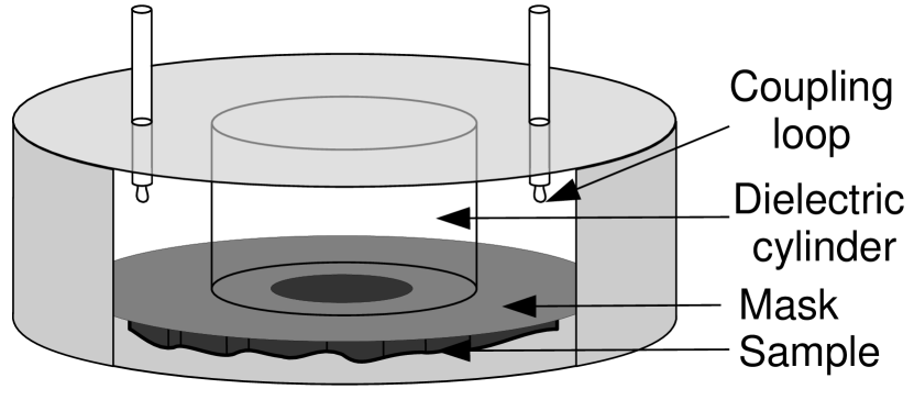
The specific dielectric resonator used here is of Hakki-Coleman type [16]. The sketch of the resonator is shown in Figure 1. The entire assembly makes use of several springs in order to avoid issues related to the thermal expansions of the different components. The resonator works in transmission, and it is excited in the TE011 mode at GHz with coaxial cables terminated with magnetic loops. A single–crystal sapphire cylindrical puck, 5.0 mm height and 8.0 mm diameter, loads the OFHC copper. Low dielectric losses ( at 9 GHz below 90 K) and relatively high permittivity (, ) [17] allows for negligible field density on the Cu walls. We note that the choice of Cu is dictated by the need to work in magnetic fields: superconducting cavities are ruled out. This constraint is detrimental to the sensitivity at low values: our setup does not reach the sensitivity needed to assess the residual at low temperature, but is instead suitable for the high–Rs regime typical of the vortex motion.
The measurements are performed in helium flow by slowly raising the temperature (0.1 K/min) after Field Cooling (FC) to the lowest temperature (typically 6 K). The field is applied perpendicular to the flat face of the sample.
Finally, in our experimental setup, the peak RF magnetic field amplitude parallel to the surface of the sample is assessed to be T. The low RF field amplitude allows a characterization of the surface impedance in the linear regime where the does not depend on the power of the applied RF field [18]. It should be noted that the surface impedance in superconductors increases with the RF field amplitude [19] and in Nb3Sn this trend is particularly accentuated (e.g. in Nb3Sn the vortex dissipation due to the trapped field increases faster than what is observed in clean Nb) [20, 19].
IV Results and discussion
The flat polycrystalline bulk Nb3Sn sample, of approximate dimensions 7 mm 5 mm, and 1 mm thick, was obtained by sintering Nb and Sn powder (25 at.%Sn) mixture under an Argon pressure of 2 kbar at 1250 ∘C in Hot Isostatic Pressure (HIP) conditions. Through X-ray diffraction methods (Rietveld refinement), the long-range order parameter was measured, showing a state of atomic ordering close to perfect ordering () [21].
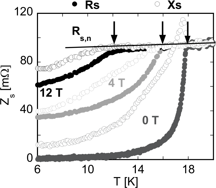
In order to check the consistency of the data on our samples with the literature, we derived the normal state resistivity from the Nb3Sn surface resistance measured above (see Figure2): cm. The measured is typical of Nb3Sn samples with and 25 at.%Sn [22, 23], entirely consistent with our results [21]. The penetration depth nm is evaluated by extrapolating T) at low temperature. The obtained value is in fair agreement with reported data [24].

The Nb3Sn surface impedance, measured in FC at T, is shown in Figure2. The beginning of the resistive transitions as a function of and are highlighted by the vertical arrows. We found that the behavior of the so-obtained is perfectly linear, and we estimate the derivative of the upper critical field near , T/K. The obtained value is fully consistent with literature [25].
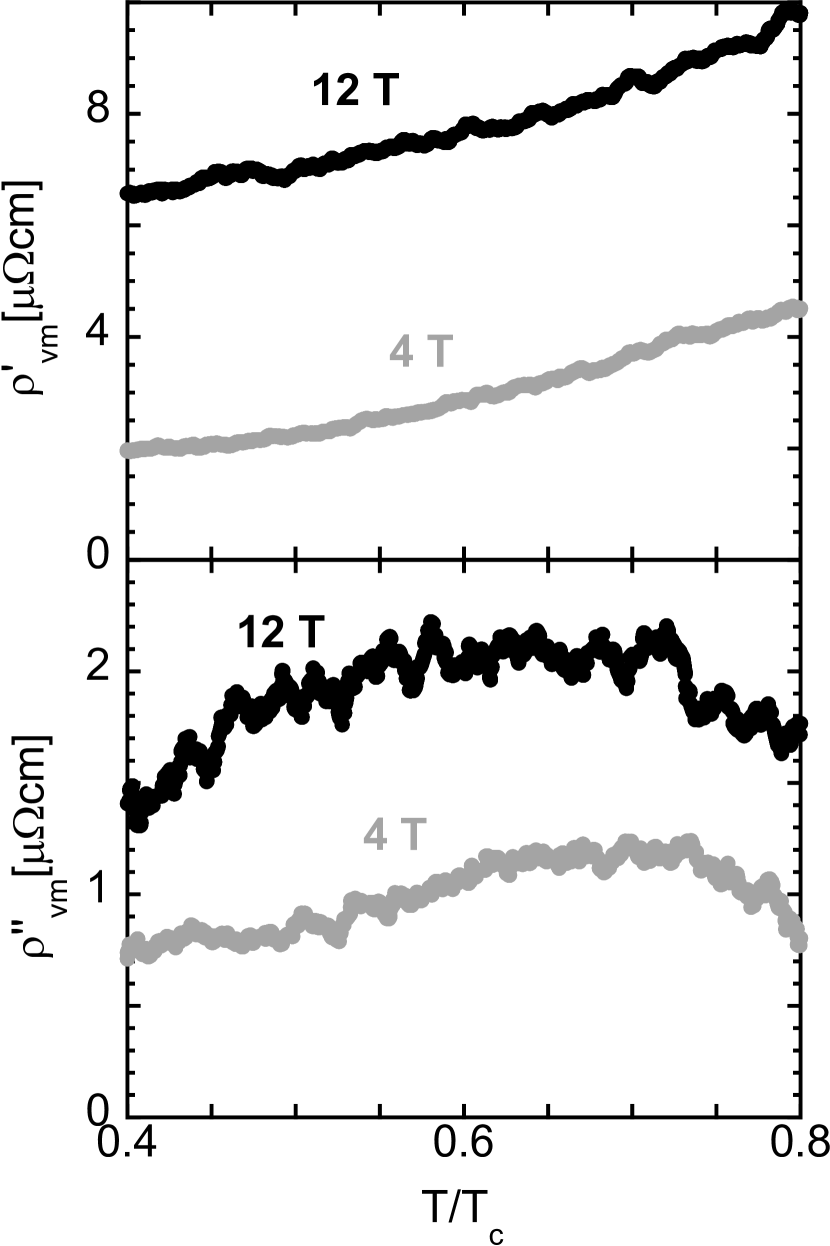
Figure 2 reports the set of measurements of . The data do not present anomalous features. It can be deduced already from the raw data that the depinning frequency is of the same order of magnitude of the measuring frequency. In fact, the increases of and with the field are different, although not much. Recalling (1), (2), one see that for both and . the increase of and should be the same. We then focus on the variations in the temperature range , in order to avoid the high– region, where thermal effects introduce additional phenomena and then model parameters. We note in passing that working with the differences allows to alleviate the potential issues concerning the sensitivity of the resonant frequency to thermal expansion. We set, consistent with our results, , and then from we isolate and . The vortex motion complex resistivity is reported in Figure 3. It is clearly seen that , although the latter is non negligible. It can be also observed that shows a tendency to decrease at high : this is completely reasonable, since at one has no imaginary part in the resistivity. Accordingly, steadily increases with . We recall that, should it be pure flux–flow (no imaginary part), the well–known Bardeen–Stephen model [26] predicts , consistent with our data.

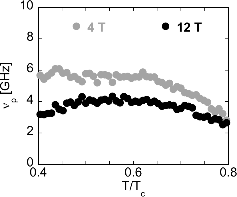
From (2) we directly derive from the data in Figure 3. The data for are reported in Figure 4. We immediately note that the values for are quite large, ranging at low from 6 GHz at 4 T to 4 GHz at 12 T. These values compare very favourably to Nb. In pure Nb films rises with the decrease of film thickness, up to GHz in 10 nm film in 0.2 T perpendicular field, but it sharply falls down to 1 GHz in 160 nm films at 5 K [27]. It can be deduced that in thick Nb films or bulks lays at best at 1 GHz, and more likely, well below. A second relevant aspect is the field resilience exhibited by Nb3Sn: is in the several GHz range in fields as high as 12 T, so that at 12 T in bulk Nb3Sn is almost 5 times that of Nb thin film (thickness 160 nm) below 1 T, demonstrating enhanced Nb3Sn RF behavior with respect to elementary Nb thin films [27, 28, 29]. Further improvements on Nb3Sn are realistically reachable with Nb3Sn thin films, where is expected to rise in analogy to Nb, opening interesting possibilities of Nb3Sn applications at microwave frequencies. In order to complete the comparison with other superconductors, we note that a comparable depinning frequency (5 GHz) is exhibited by 13 m thickness foils of Pb0.83In0.17 at 1.7 K and 0.5 [10]. Cuprates are known to have large depinning frequency [30, 31], with high values in YBa2Cu3O7-x (YBCO) single crystal, about GHz at 45 K [30, 31]. YBCO thin films with BaZrO3 columnar and elongated defects exhibits still enhanced pinning frequencies: GHz at 70 K [32]. However, it must be mentioned that, at least in Tl2Ba2Ca2CuO8+x, such high are anomalously accompanied by a very large dissipation [33].
We make a final note on the possible effects of thermal activation (flux–creep). Should it be present, the effect is to reduce and to increase : the more the thermal creep is prominent the more the pinning effect vanishes and [12, 14]. From (2) and measurement frequency , it can be shown that this phenomenon is modeled as a first approximation with a lowering of in (2) in order to obtain the same creep-induced increase in and reduction of . Thus within this model, the obtained is at worst an underestimate. For this reason, we can state that our measurements set a lower limit to the Nb3Sn depinning frequency (Figure 4) without the need for entering any other parameter (i.e. the creep factor). Therefore, this result is robust against the possible presence of flux–creep: the depinning frequency remains rather high in Nb3Sn, much higher than in Nb.

V Conclusion
We presented the first microwave ( GHz) characterization of Nb3Sn in high magnetic fields (up to 12 T). The Nb3Sn surface impedance was evaluated in the mixed state to obtain information about the dissipative and reactive phenomena of vortex motion. From elaborations we obtained and showed the vortex motion complex resistivity, a quantity that directly allowed us to obtain the depinning frequency of Nb3Sn. The depinning frequency is a parameter of great relevance because it establishes the frequency above which the elastic RF vortex motion becomes purely resistive. Hence, is the highest theoretical working frequency for low loss RF applications in high magnetic fields.
The measured is almost constant in temperature (up to ) and decreases from 6.0 GHz at 4 T, to 4.5 GHz at 12 T. This result shows that the Nb3Sn exhibits much better RF characteristics than Nb and encourages the use of Nb3Sn in technological RF and mw applications up to few GHz also in presence of dc magnetic fields.
References
- [1] X. Xu, “A review and prospects for Nb3Sn superconductor development,” Supercond. Sci. Technol., vol. 30, no. 9, p. 093001, Aug 2017.
- [2] R. J. Thome, I. J. Central, and H. Teams, “Design & development of the ITER magnet system,” Cryogenics, vol. 34, pp. 39–46, May. 1994.
- [3] S. Posen and D. L. Hall, “Nb3Sn superconducting radiofrequency cavities: fabrication, results, properties, and prospects,” Supercond. Sci. Technol., vol. 30, no. 3, p. 033004, Jan. 2017.
- [4] A. M. Valente-Feliciano, “Superconducting RF materials other than bulk niobium: a review,” Supercond. Sci. Technol., vol. 29, no. 11, p. 113002, Sep. 2016.
- [5] H. Padamsee, J. Knobloch, and T. Hays, RF Superconductivity for Accelerators. Wiley-VCH, 1998.
- [6] R. Flükiger, “Overview of superconductivity and challenges in applications,” Rev. Accel Sci. Technol., vol. 5, pp. 1–23, Apr. 2012.
- [7] H. Padamsee, RF superconductivity: science, technology, and applications. John Wiley & Sons, 2009.
- [8] C. Becker, S. Posen et al., “Analysis of Nb3Sn surface layers for superconducting radio frequency cavity applications,” Appl. Phys. Lett., vol. 106, no. 8, p. 082602, Feb. 2015.
- [9] A. Grassellino, A. Romanenko et al., “Accelerating fields up to 49 MV/m in TESLA-shape superconducting RF niobium cavities via 75C vacuum bake,” arXiv preprint arXiv:1806.09824, Jun. 2018.
- [10] J. I. Gittleman and B. Rosenblum, “Radio-frequency resistance in the mixed state for subcritical currents,” Phys. Rev. Lett., vol. 16, no. 17, p. 734, Apr. 1966.
- [11] R. E. Collin, Foundations for microwave engineering. John Wiley & Sons, 2007.
- [12] M. W. Coffey and J. R. Clem, “Unified theory of effects of vortex pinning and flux creep upon the RF surface impedance of type-II superconductors,” Phys. Rev. Lett., vol. 67, no. 3, p. 386, 1991.
- [13] M. Tinkham, Introduction to superconductivity. Courier Corporation, 1996.
- [14] N. Pompeo and E. Silva, “Reliable determination of vortex parameters from measurements of the microwave complex resistivity,” Phys. Rev. B, vol. 78, no. 9, p. 094503, Sep. 2008.
- [15] L.-F. Chen, C. Ong et al., Microwave electronics: measurement and materials characterization. John Wiley & Sons, 2004.
- [16] B. Hakki and P. Coleman, “A dielectric resonator method of measuring inductive capacities in the millimeter range,” IRE Trans. Microwave Theory and Tech., vol. 8, no. 4, pp. 402–410, Sep. 1960.
- [17] V. Braginsky, V. Ilchenko, and K. S. Bagdassarov, “Experimental observation of fundamental microwave absorption in high-quality dielectric crystals,” Phys. Lett. A, vol. 120, no. 6, pp. 300–305, Mar. 1987.
- [18] H. Weinstock and M. Nisenoff, Microwave superconductivity. Springer Science & Business Media, 2012, vol. 375.
- [19] M. Martinello, A. Grassellino et al., “Effect of interstitial impurities on the field dependent microwave surface resistance of niobium,” Appl. Phys. Lett., vol. 109, no. 6, p. 062601, Aug. 2016.
- [20] D. Hall, J. Kaufman et al., “First results from new single-cell Nb3Sn cavities coated at Cornell University,” in Proc. of International Particle Accelerator Conference (IPAC’17), May 2017, pp. 40–43.
- [21] T. Spina, Proton irradiation effects on Nb3Sn wires and thin platelets in view of High Luminosity LHC upgrade. Ph.D thesis in Physics, Universite de Geneve, Deparement de Physique de la Matiere Quantique (DQMP), 2015.
- [22] R. Flukiger, H. Kupfer et al., “Effect of atomic ordering and composition changes on the electrical resistivity of Nb3Al, Nb3Sn, Nb3Ge, Nb3Ir, V3Si and V3Ga,” IEEE Trans. Magn., vol. 23, no. 2, pp. 980–983, Mar. 1987.
- [23] A. Godeke, “A review of the properties of Nb3Sn and their variation with A15 composition, morphology and strain state,” Supercond. Sci. Technol., vol. 19, no. 8, p. R68, Jun. 2006.
- [24] Y. Li and Y. Gao, “GLAG theory for superconducting property variations with A15 composition in Nb3Sn wires,” Sci. Rep., vol. 7, no. 1, p. 1133, Apr. 2017.
- [25] T. P. Orlando, E. J. McNiff et al., “Critical fields, Pauli paramagnetic limiting, and material parameters of Nb3Sn and Si,” Phys. Rev. B, vol. 19, pp. 4545–4561, May. 1979.
- [26] J. Bardeen and M. J. Stephen, “Theory of the motion of vortices in superconductors,” Phys. Rev., vol. 140, pp. A1197–A1207, Nov. 1965.
- [27] D. Janjušević, M. S. Grbić et al., “Microwave response of thin niobium films under perpendicular static magnetic fields,” Phys. Rev. B, vol. 74, no. 10, p. 104501, Sep. 2006.
- [28] N. Pompeo, K. Torokhtii et al., “Superconducting and Structural Properties of Nb/PdNi/Nb Trilayers,” J. Supercond. Novel Magn., vol. 26, no. 5, pp. 1939–1943, May. 2013.
- [29] E. Silva, N. Pompeo, and S. Sarti, “Wideband microwave measurements in Nb/Pd84Ni16/Nb structures and comparison with thin Nb films,” Supercond. Sci. Technol., vol. 24, no. 2, p. 024018, Jan. 2011.
- [30] M. Golosovsky, M. Tsindlekht, and D. Davidov, “High-frequency vortex dynamics in YBa2Cu3O7,” Supercond. Sci. Technol., vol. 9, no. 1, p. 1, Sep. 1996.
- [31] Y. Tsuchiya, K. Iwaya et al., “Electronic state of vortices in YBa2Cu3Oy investigated by complex surface impedance measurements,” Phys. Rev. B, vol. 63, no. 18, p. 184517, Apr. 2001.
- [32] K. Torokhtii, N. Pompeo et al., “Measurement of vortex pinning in YBCO and YBCO/BZO coated conductors using a microwave technique,” IEEE Trans. Appl. Supercond., vol. 26, no. 3, p. 8001605, Apr. 2016.
- [33] N. Pompeo, H. Schneidewind, and E. Silva, “Measurements of microwave vortex response in dc magnetic fields in Tl2Ba2CaCu2O8+x films,” presented at ASC 2018, abstract no. 2985707, submitted for publication.