Epitaxial single layer NbS2 on Au(111): synthesis, structure, and electronic properties
Abstract
We report on the epitaxial growth of single layer NbS2 on Au(111) and determine both its crystalline and electronic structure by a combination of low-energy electron diffraction, scanning tunnelling microscopy and angle-resolved photoemission spectroscopy. The layer is found to grow in the 1H structural phase with a lattice constant of (3.290.03) Å, a value comparable to the bulk 2H NbS2 lattice constant. The photoemission data reveals a metallic band structure down to a temperature of 30 K. The observed bands are rather broad and consistent with either a strong NbS2-substrate interaction or with the recently reported interplay of strong many-body effects in single layer NbS2 van Loon et al. (2018). No indications of a charge density wave are observed.
I Introduction
Metallic transition metal dichalcogenides (TMDCs) have been studied for decades due to their susceptibility to many fascinating quantum states, such as charge and spin ordering, Mott insulating states, and superconductivity; and because, more generally, they provide a platform for the study of many-body interactions in nearly two-dimensional (2D) materials Wilson and Yoffe (1969); Wilson et al. (1975); Rossnagel (2011). The ability to isolate single layer (SL) TMDCs Mak et al. (2010); Novoselov et al. (2005); Splendiani et al. (2010) now extends these types of investigations to genuinely 2D systems. This avenue of research is rather compelling, especially since it has turned out that the assumption of a purely 2D character in van der Waals bonded bulk compounds may not be generally valid, after all Di Sante et al. (2017); Ngankeu et al. (2017). Moreover, the properties of SL materials may be tuned by the choice of substrate, as this interaction can have a significant impact on the electronic properties of the 2D material, for instance, by screening the otherwise strongly enhanced Coulomb interaction Ugeda et al. (2014); Qiu et al. (2013); Grubišić Čabo et al. (2015); Rösner et al. (2016). Studies of metallic SL TMDCs are considerably more challenging than of their semiconducting counterparts, such as MoS2, due to their strongly enhanced chemical reactivity, which may also be responsible for the partly contradictory results on, for example, the superconducting transition temperature in atomically thin 2H TaS2 Galvis et al. (2014); Navarro-Moratalla et al. (2016); Peng et al. (2018) or the charge density wave (CDW) transition temperature in SL NbSe2 Xi et al. (2015); Ugeda et al. (2016).
The isoelectronic sulphides and selenides of vandium, niobium and tantalum show an intriguing competition between magnetism, charge density waves and Mott insulating behaviour. It is not unusual for several of these quantum states to be observed in the same material at different temperatures or even simultaneously. 2H NbS2 stands out in this class of materials because it is widely considered to be the only case for which superconductivity can be observed (6 K) in the absence of charge density wave states Naito and Tanaka (1982); Guillamón et al. (2008); Heil et al. (2017) (even though this long-held point of view has recently been called into question Leroux et al. (2018)).
While few layer (3R) Kozhakhmetov et al. (2018) and even single layer NbS2 Bark et al. (2018) have been successfully synthesized, little is known about the different ground states in SL NbS2. Density functional theory and GW calculations predict SL NbS2 to be metallic with a half-filled upper valence band that is well-separated from other electronic states Kuc et al. (2011); Heil et al. (2018). In this approximation, the ground state of the system is not magnetic but it is close to magnetic phases Zhou et al. (2012); Güller et al. (2016). Very recently, the electronic structure of SL NbS2 was studied with the inclusion of several types of many-body effects, such as short- and long-range Coulomb interactions, and electron-phonon interactions van Loon et al. (2018). The study found that each of these interactions has a significant effect on the spectral function, leading to situations that are drastically different from the bare single particle dispersion. Rather unexpectedly, the combined effect of the many-body interactions restores the spectral function to what essentially resembles a broadened version of the bare dispersion. From these results, SL NbS2 might be expected to be a unique case for experimentally tuning different many-body interactions by, for example, the choice of doping or substrate, in order to reach a multitude of desired ground states.
In this Article, we report on the synthesis of SL NbS2 on Au(111). Due to the epitaxial character of the system, the growth is restricted to a single orientation (and its mirror domain), thereby allowing both the crystalline and electronic structure of the SL NbS2 to be probed with spatially averaging techniques such as low-energy electron diffraction (LEED) and angle-resolved photoemission spectroscopy (ARPES). Consistent with a strong NbS2-Au(111) interaction, or with an interplay of strong many-body effects in the SL NbS2 van Loon et al. (2018), or with a combination of both, the ARPES data divulges a metallic band structure with broad bands.
II Experimental
The growth of epitaxial SL NbS2 on Au (111) was based on a growth technique previously developed for other SL TMDCs Lauritsen et al. (2007); Füchtbauer et al. (2014); Miwa et al. (2015); Dendzik et al. (2015); Sanders et al. (2016); Arnold et al. (2018), with the transition metal being evaporated onto a single-crystal in a sulphur-rich atmosphere. Initially the Au(111) substrate (Mateck) was cleaned by repeated cycles of ion bombardment (Ne+ at 1.5 keV) and annealing to 650 °C under ultrahigh vacuum (UHV) conditions. The surface order and cleanliness were established by scanning tunnelling microscopy (STM); the substrate was sputtered and annealed until STM revealed an atomically clean surface with the characteristic herringbone reconstruction Barth et al. (1990). Niobium was evaporated from an electron beam evaporator (Nb rod of 99.9 purity from Goodfellow) onto the clean Au(111) surface, held at room temperature, in a pressure of 210-6 mbar of dimethyl disulphide (DMDS, C2H6S2, with 99 % purity from Sigma-Aldrich). The sample was subsequently annealed for 30 min at 450 °C while the same pressure of DMDS was maintained. Finally, the DMDS was pumped out of the chamber and the sample was annealed to 600 °C for 30 min in order to eliminate residual physisorbed DMDS, and to improve the overall crystalline quality of the SL NbS2.
Synthesis and STM characterization of the SL NbS2 growth were performed in a dedicated growth chamber (base pressure of 10-10 mbar) using a home-built Aarhus-type STM Besenbacher et al. (1988). Tips were made from a Pt-Ir alloy. All STM images were processed using free WSxM software Horcas et al. (2007) and generally involved plane flattening and calibrating to reflect the known atomic lattice parameter of the clean Au(111) surface. The uncertainties associated with the quoted lengths determined by STM arise mainly from thermal drift and/or piezo creep. LEED and ARPES measurements were performed at the SGM3 beamline at the ASTRID2 synchrotron radiation facility Hoffmann et al. (2004). ARPES and LEED data were collected at 30 K. All ARPES measurements presented here were performed with a photon energy of 50 eV with an energy and angular resolution better than 25 meV and 0.2 °, respectively.
To transfer the reactive SL NbS2, in air, from the growth/STM chamber to the ARPES/LEED chamber, the sample was protected by a DMDS capping layer. The capping layer was prepared by keeping the grown SL NbS2 sample at room temperature in a DMDS pressure of 210-6 mbar for 30 min. Once the sample was reintroduced to UHV conditions at the SGM3 beamline, it was annealed to 600 °C for 30 min to remove the physisorbed capping layer. STM images were acquired after the removal of the capping layer in the ARPES chamber (not shown), and were consistent with a surface cleanliness on par with SL NbS2 samples grown without a capping layer.
III Results and Discussion

Figure 1(a) shows the topography of SL NbS2 on Au(111) measured by STM. Several domains of SL NbS2 are visible with smaller regions of clean Au in between. Although not visible in the STM image presented here, the dark regions between the SL NbS2 domains are identified as clean Au because either Au atoms and/or a typically distorted herringbone structure are observed Grønborg et al. (2015). The SL NbS2 domains cover approximately 75 % of the surface, and are irregular in shape with sharp boundaries between adjacent domains. A well-ordered hexagonal moiré is visible, due to the different periodicity of the substrate and the epitaxial layer. The periodicity of the moiré is 20.7 Å, as determined from Fourier transform analysis of the STM data. The moiré pattern is qualitatively very similar to that observed for other epitaxial SL TMDCs on Au(111), particularly MoS2, WS2, and TaS2 Grønborg et al. (2015); Dendzik et al. (2015); Sanders et al. (2016); and the minor distortions in the regularity of the moiré, especially close to edges and domain boundaries, can be understood in terms of local strain in the material Zhang et al. (2018).
Figure 1(b) shows an atomically resolved image from which a hexagonal lattice constant of (3.40.3) Å was extracted. This value is in agreement with the bulk lattice parameter of 3.3 Å for 2H NbS2 Wilson and Yoffe (1969). It is not straightforward, on the basis of atomically-resolved STM images alone, to distinguish between the possible polymorphs of the SL structure, which are either trigonal prismatic (1H) or octahedral (1T), since both polymorphs possess a hexagonal structure with presumably similar lattice constants.
Figure 1(c) shows a line profile taken across the edge of a domain boundary. The profile reveals an apparent height difference of (3.10.2) Å between the top of the NbS2 layer and the Au(111) surface. This value is consistent with the results for similar systems Grønborg et al. (2015); Dendzik et al. (2015); Sanders et al. (2016).
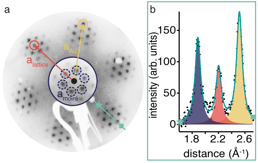
The overall ordering on the surface can be studied by LEED. Figure 2(a) shows a LEED pattern revealing the integer order diffraction spots of both the NbS2 (red circle) and the Au(111) lattice (yellow circle) and the additional spots due to the moiré (dashed blue circle). The two main lattices are well aligned and only one orientation of the SL NbS2 is observed, albeit with the possibility of mirror domains Bana et al. (2018). An accurate determination of the SL NbS2 lattice parameter can be achieved by fitting the peak positions in a line cut through the image, as shown in Figure 2(b). The cut was taken along the green line from the star to the square. The known 2.88 Å lattice parameter of Au(111) was used as a calibration, and from the analyses of this and similar cuts in the corresponding directions, the lattice parameter of SL NbS2 was determined to be (3.290.03) Å, in agreement with the STM results. We note that we do not observe any additional spots in the LEED that could hint at the existence of a charge density wave in SL NbS2 at 30 K.
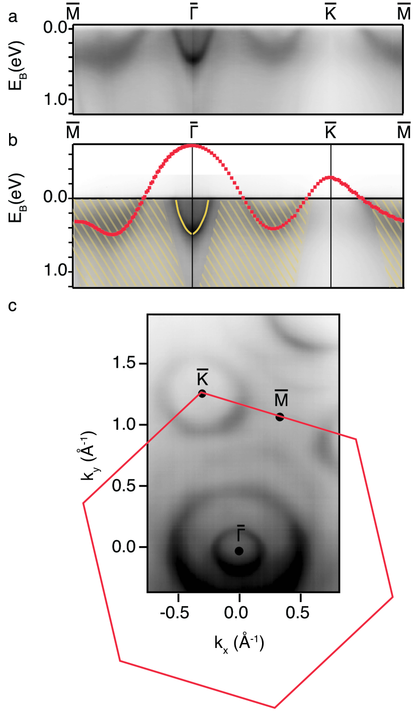
Finally, we determine the electronic structure of SL NbS2 using ARPES. The photoemission intensity along the high symmetry directions of the NbS2 2D Brillouin zone, acquired with 50 eV photons, is shown in Figure 3(a). The same data is reproduced in Figure 3(b) but with salient features marked. Some features crossing the Fermi level can be assigned to the well-known Au(111) surface state around LaShell et al. (1996) and the -bulk band of Au (very weak). The other visible features stem from SL NbS2: a hole pocket around and a second hole pocket around (). The parabolic Au(111) surface state is marked by the yellow line. The yellow striped and shaded region indicates the projected bulk bands of Au(111). Overlaid on the data, in red, is the calculated bare dispersion for SL NbS2 recently reported in Ref. van Loon et al. (2018). From this ARPES data, we conclude that SL NbS2 is metallic and that the general shape of the band structure is consistent with that expected for the 1H polytype Kuc et al. (2011); Heil et al. (2018). The band structure is essentially the same as observed for SL TaS2 but without the strong spin-orbit splitting Sanders et al. (2016).
The calculated band structure has been rigidly shifted by 0.15 eV to higher binding energies in order to attain an approximate agreement between measurement and calculation; however, there is no rigid shift of the calculated band structure that can provide complete agreement with the measured data. Perhaps the lack of quantitative agreement is not entirely surprising, as almost the entire observed band structure falls with the projected bulk bands of Au(111) Takeuchi et al. (1991) and therefore some hybridization with the substrate is expected to occur Bruix et al. (2016); Dendzik et al. (2017); Shao et al. (in press). On the other hand, in the very similar case of SL TaS2 on Au(111), an excellent agreement between calculated and observed bands can be achieved by a rigid energy shift Sanders et al. (2016). Lastly, we note that there are no indications of gap openings or back-folding of bands in Figure 3(a), as might be expected in the presence of a CDW.
The photoemission intensity at the Fermi energy is shown in Figure 3(c) with the high symmetry points indicated and the NbS2 2D Brillouin zone superimposed on the ARPES data in red. From the size of the Fermi contour, the electron filling of the SL NbS2 valence band can be estimated. Using the same approach as in Ref. Sanders et al. (2016), we determine that the upper valence band of SL NbS2 on Au(111) is filled by 1.360.02 electrons per unit cell instead of the expected one electron. This corresponds to an electron concentration of (1.260.02) cm-2. Such strong doping effects have also been observed for SL TaS2 on Au(111) Sanders et al. (2016). In that case, they are not necessarily caused by true doping of the SL material and can rather be explained by hybridization-induced “pseudo-doping” Shao et al. (in press). This is also likely to be the case here.
Despite the excellent crystalline quality revealed by STM and LEED, the SL NbS2-related features observed in ARPES are very broad in contrast to the results from other other high-quality SL TMDCs. One possible reason for this is the hybridization between SL and substrate states Bruix et al. (2016); Dendzik et al. (2017). Indeed, very sharp bands can only be observed in the case of semiconducting SL TMDCs on Au(111) or Ag(111) for the specific spectral region around the valence band maximum at due to position of this band in a projected band gap of the substrate Hinsche et al. (2017); Mahatha et al. (2019). Here, the SL NbS2 valence band maximum at is above the Fermi energy, almost the entire observed band structure falls in the continuum of the Au bulk states, and is thus prone to hybridization. Another possible explanation for the broad bands is the many-body interactions discussed in Ref. van Loon et al. (2018) that lead to a substantial broadening of the spectral function for the free-standing material. The calculated theoretical linewidth in Ref. van Loon et al. (2018) is of the same order as the experimental values observed here. However, the additional interaction with the substrate makes a detailed analysis difficult.
IV Conclusions
In summary, we have reported the epitaxial growth of SL NbS2 on Au(111). Excellent structural quality can be realized, as revealed by STM and LEED. The resulting band structure is consistent with a 1H crystalline structure. It reveals strong electron doping that could partly be due to hybridization with the substrate, as previously reported for SL TaS2 Sanders et al. (2016); Shao et al. (in press). In contrast to the occupied band structure of SL TaS2 on Au(111), however, clear deviations between the observed band structure and the rigidly shifted calculated bands for a free-standing layer are seen. Finally, the observed spectral features are rather broad. This could also be due to hybridization or to the predicted strong many-body interactions in this system van Loon et al. (2018). This could perhaps be investigated further by transferring the growth procedure described here to a more inert substrate or, possibly, by intercalation-induced decoupling of the NbS2 layer from the substrate Mahatha et al. (2019).
V Acknowledgements
We thank the authors of Ref. van Loon et al. (2018) for helpful discussions and for making their data available to us. This work was supported by the Danish Council for Independent Research, Natural Sciences under the Sapere Aude program (Grants No. DFF-4002-00029 and DFF-6108-00409) and by VILLUM FONDEN via the Centre of Excellence for Dirac Materials (Grant No. 11744) and the Aarhus University Research Foundation. Affiliation with the Center for Integrated Materials Research (iMAT) at Aarhus University is gratefully acknowledged.
References
- van Loon et al. (2018) E. G. C. P. van Loon, M. Rösner, G. Schönhoff, M. I. Katsnelson, and T. O. Wehling, npj Quantum Materials 3, 32 (2018)
- Wilson and Yoffe (1969) J. Wilson and A. Yoffe, Advances in Physics 18, 193 (1969)
- Wilson et al. (1975) J. Wilson, F. Di Salvo, and S. Mahajan, Advances in Physics 24 117 (1975),
- Rossnagel (2011) K. Rossnagel, Journal of Physics: Condensed Matter 23, 213001 (2011)
- Mak et al. (2010) K. F. Mak, C. Lee, J. Hone, J. Shan, and T. F. Heinz, Phys. Rev. Lett. 105, 136805 (2010)
- Novoselov et al. (2005) K. S. Novoselov, D. Jiang, F. Schedin, T. J. Booth, V. V. Khotkevich, S. V. Morozov, and A. K. Geim, Proceedings of the National Academy of Sciences of the United States of America 102, 10451 (2005)
- Splendiani et al. (2010) A. Splendiani, L. Sun, Y. Zhang, T. Li, J. Kim, C.-Y. Chim, G. Galli, and F. Wang, Nano Letters 10, 1271 (2010)
- Di Sante et al. (2017) D. Di Sante, P. K. Das, C. Bigi, Z. Ergönenc, N. Gürtler, J. A. Krieger, T. Schmitt, M. N. Ali, G. Rossi, R. Thomale, et al., Phys. Rev. Lett. 119, 026403 (2017)
- Ngankeu et al. (2017) A. S. Ngankeu, S. K. Mahatha, K. Guilloy, M. Bianchi, C. E. Sanders, K. Hanff, K. Rossnagel, J. A. Miwa, C. Breth Nielsen, M. Bremholm, et al., Phys. Rev. B 96, 195147 (2017)
- Ugeda et al. (2014) M. M. Ugeda, A. J. Bradley, S.-F. Shi, F. H. da Jornada, Y. Zhang, D. Y. Qiu, W. Ruan, S.-K. Mo, Z. Hussain, Z.-X. Shen, et al., Nat Mater 13, 1091 (2014)
- Qiu et al. (2013) D. Y. Qiu, F. H. da Jornada, and S. G. Louie, Phys. Rev. Lett. 111, 216805 (2013)
- Grubišić Čabo et al. (2015) A. Grubišić Čabo, J. A. Miwa, S. S. Grønborg, J. M. Riley, J. C. Johannsen, C. Cacho, O. Alexander, R. T. Chapman, E. Springate, M. Grioni, et al., Nano Letters 15, 5883 (2015)
- Rösner et al. (2016) M. Rösner, C. Steinke, M. Lorke, C. Gies, F. Jahnke, and T. O. Wehling, Nano Letters 16, 2322 (2016)
- Galvis et al. (2014) J. A. Galvis, L. Chirolli, I. Guillamón, S. Vieira, E. Navarro-Moratalla, E. Coronado, H. Suderow, and F. Guinea, Phys. Rev. B 89, 224512 (2014)
- Navarro-Moratalla et al. (2016) E. Navarro-Moratalla, J. O. Island, S. Manas-Valero, E. Pinilla-Cienfuegos, A. Castellanos-Gomez, J. Quereda, G. Rubio-Bollinger, L. Chirolli, J. A. Silva-Guillen, N. Agrait, et al., Nat Commun 7 (2016)
- Peng et al. (2018) J. Peng, Z. Yu, J. Wu, Y. Zhou, Y. Guo, Z. Li, J. Zhao, C. Wu, and Y. Xie, ACS Nano (2018)
- Xi et al. (2015) X. Xi, L. Zhao, Z. Wang, H. Berger, L. Forró, J. Shan, and K. F. Mak, Nature Nanotechnology 10, 765 (2015)
- Ugeda et al. (2016) M. M. Ugeda, A. J. Bradley, Y. Zhang, S. Onishi, Y. Chen, W. Ruan, C. Ojeda-Aristizabal, H. Ryu, M. T. Edmonds, H.-Z. Tsai, et al., Nat Phys 12, 92 (2016)
- Naito and Tanaka (1982) M. Naito and S. Tanaka, Journal of the Physical Society of Japan 51, 219 (1982)
- Guillamón et al. (2008) I. Guillamón, H. Suderow, S. Vieira, L. Cario, P. Diener, and P. Rodière, Phys. Rev. Lett. 101, 166407 (2008)
- Heil et al. (2017) C. Heil, S. Poncé, H. Lambert, M. Schlipf, E. R. Margine, and F. Giustino, Phys. Rev. Lett. 119, 087003 (2017)
- Leroux et al. (2018) M. Leroux, L. Cario, A. Bosak, and P. Rodière, Phys. Rev. B 97, 195140 (2018)
- Kozhakhmetov et al. (2018) A. Kozhakhmetov, T. H. Choudhury, Z. Y. A. Balushi, M. Chubarov, and J. M. Redwing, Journal of Crystal Growth 486, 137 (2018)
- Bark et al. (2018) H. Bark, Y. Choi, J. Jung, J. H. Kim, H. Kwon, J. Lee, Z. Lee, J. H. Cho, and C. Lee, Nanoscale 10, 1056 (2018)
- Kuc et al. (2011) A. Kuc, N. Zibouche, and T. Heine, Phys. Rev. B 83, 245213 (2011)
- Heil et al. (2018) C. Heil, M. Schlipf, and F. Giustino, Phys. Rev. B 98, 075120 (2018)
- Zhou et al. (2012) Y. Zhou, Z. Wang, P. Yang, X. Zu, L. Yang, X. Sun, and F. Gao, ACS Nano 6, 9727 (2012)
- Güller et al. (2016) F. Güller, V. L. Vildosola, and A. M. Llois, Phys. Rev. B 93, 094434 (2016)
- Lauritsen et al. (2007) J. V. Lauritsen, J. Kibsgaard, S. Helveg, H. Topsoe, B. S. Clausen, E. Laegsgaard, and F. Besenbacher, Nature Nanotechnology 2, 53 (2007)
- Füchtbauer et al. (2014) H. Füchtbauer, A. Tuxen, Z. Li, H. Topsøe, J. Lauritsen, and F. Besenbacher, 57, 207 (2014)
- Miwa et al. (2015) J. A. Miwa, S. Ulstrup, S. G. Sørensen, M. Dendzik, A. G. Čabo, M. Bianchi, J. V. Lauritsen, and P. Hofmann, Phys. Rev. Lett. 114, 046802 (2015)
- Dendzik et al. (2015) M. Dendzik, M. Michiardi, C. Sanders, M. Bianchi, J. A. Miwa, S. S. Grønborg, J. V. Lauritsen, A. Bruix, B. Hammer, and P. Hofmann, Phys. Rev. B 92, 245442 (2015)
- Sanders et al. (2016) C. E. Sanders, M. Dendzik, A. S. Ngankeu, A. Eich, A. Bruix, M. Bianchi, J. A. Miwa, B. Hammer, A. A. Khajetoorians, and P. Hofmann, Phys. Rev. B 94, 081404 (2016)
- Arnold et al. (2018) F. Arnold, R.-M. Stan, S. K. Mahatha, H. E. Lund, D. Curcio, M. Dendzik, H. Bana, E. Travaglia, L. Bignardi, P. Lacovig, et al., 2D Materials 5, 045009 (2018)
- Barth et al. (1990) J. V. Barth, H. Brune, G. Ertl, and R. J. Behm, Physical Review B 42, 9307 (1990)
- Besenbacher et al. (1988) F. Besenbacher, E. Lægsgaard, K. Mortensen, U. Nielsen, and I. Stensgaard, Rev. Sci. Instrum. 59, 1035 (1988)
- Horcas et al. (2007) I. Horcas, R. Fernández, J. M. Gómez-Rodríguez, J. Colchero, J. Gómez-Herrero, and A. M. Baro, Review of Scientific Instruments 78, 013705 (2007)
- Hoffmann et al. (2004) S. V. Hoffmann, C. Søndergaard, C. Schultz, Z. Li, and P. Hofmann, Nuclear Instruments and Methods in Physics Research, A 523, 441 (2004)
- Grønborg et al. (2015) S. S. Grønborg, S. Ulstrup, M. Bianchi, M. Dendzik, C. E. Sanders, J. V. Lauritsen, P. Hofmann, and J. A. Miwa, Langmuir 31, 9700 (2015)
- Zhang et al. (2018) C. Zhang, M.-Y. Li, J. Tersoff, Y. Han, Y. Su, L.-J. Li, D. A. Muller, and C.-K. Shih, Nature Nanotechnology 13, 152 (2018)
- Bana et al. (2018) H. Bana, E. Travaglia, L. Bignardi, P. Lacovig, C. E. Sanders, M. Dendzik, M. Michiardi, M. Bianchi, D. Lizzit, F. Presel, et al., 2D Materials 5, 035012 (2018)
- LaShell et al. (1996) S. LaShell, B. A. McDougall, and E. Jensen, Physical Review Letters 77, 3419 (1996)
- Takeuchi et al. (1991) N. Takeuchi, C. T. Chan, and K. M. Ho, Phys. Rev. B 43, 13899 (1991)
- Bruix et al. (2016) A. Bruix, J. A. Miwa, N. Hauptmann, D. Wegner, S. Ulstrup, S. S. Grønborg, C. E. Sanders, M. Dendzik, A. Grubišić Čabo, M. Bianchi, et al., Phys. Rev. B 93, 165422 (2016)
- Dendzik et al. (2017) M. Dendzik, A. Bruix, M. Michiardi, A. S. Ngankeu, M. Bianchi, J. A. Miwa, B. Hammer, P. Hofmann, and C. E. Sanders, Physical Review B 96, 235440 (2017)2469-9969,
- Shao et al. (in press) B. Shao, A. Eich, C. Sanders, A. S. Ngankeu, M. Bianchi, P. Hofmann, A. A. Khajetoorians, and T. O. Wehling, Nature Communications (in press).
- Hinsche et al. (2017) N. F. Hinsche, A. S. Ngankeu, K. Guilloy, S. K. Mahatha, A. Grubišić Čabo, M. Bianchi, M. Dendzik, C. E. Sanders, J. A. Miwa, H. Bana, et al., Physical Review B 96, 121402 (2017), ISSN 2469-9969
- Mahatha et al. (2019) S. K. Mahatha, A. S. Ngankeu, N. F. Hinsche, I. Mertig, K. Guilloy, P. L. Matzen, M. Bianchi, C. E. Sanders, J. A. Miwa, H. Bana, et al., Surface Science 681, 64 (2019)