ORCID: ]https://orcid.org/0000-0001-9218-1678 ORCID: ]https://orcid.org/0000-0002-3176-8042 ORCID: ]https://orcid.org/0000-0001-5873-7476
Theory of electron transport and emission from a semiconductor nanotip
Abstract
An effective mass based model accounting for the conduction band quantization in a high aspect ratio semiconductor nanotip is developed to describe injected electron transport and subsequent electron emission from the nanotip. A transfer matrix formalism is used to treat electron scattering induced by the variation in the tip diameter and the electron emission. Numerical analysis of the scattering and emission probabilities is performed for the diamond parametrized nanotip model. Our scattering and emission models are further combined with a Monte Carlo (MC) approach to simulate electron transport through the nanotip. The MC simulations, also accounting for the electron-phonon scattering and externally applied electric field, are performed for a minimal nanotip model and an equivalent width diamond slab. An effect of the level quantization, electron scattering due to the nanotip diameter variation, and electron-phonon scattering on the nanotip emission properties is identified and compared with the case of bulk slab.
I Introduction
Nanostructured cold cathodes are required for applications in flat panel displays,Choi et al. (1999); Wang et al. (2001); Chandrasekhar (2018) flat panel X-ray sources,Posada et al. (2014) microwave devices,Teo et al. (2005) free-electron lasers and accelerators.Li et al. (2013); Baryshev et al. (2014) Recent progress towards developing a new class of table top free-electron light sources and accelerators imposed a high demand in new cathode technologies.Adamo et al. (2009); Peralta et al. (2013); Wong et al. (2015); Zhao et al. (2018) These accelerators are driven by infrared lasers and their dimensions are 2-3 orders of magnitude smaller than the dimensions of their radio frequency counterparts. Therefore, high brightness cold or photo cathodes with the capability to produce low divergence and small emittance beams on the nanometer to micron scale are desirable. In light of this, nanotip based electron emission sources are natural candidates for the production of high current electron beams. Recently, carbon nanotube based field emitters have been extensively studied due to their unique charge carrier transport, emission characteristics, and well developed fabrication and characterization technologies.Bocharov and Eletskii (2013); Chandrasekhar (2018); Choi et al. (1999); De Heer et al. (1995); Maiti et al. (2001); Teo et al. (2005); Bocharov and Eletskii (2013) Besides carbon nanotubes, the field emission has been studies in nanoparticles,Di Bartolomeo et al. (2016) nanowires (NWs),Zhi et al. (2005); Giubileo et al. (2017) and graphene.Wu et al. (2009); Shao and Khursheed (2018)
Diamond naturally plays a central role in developing cold cathodes due to possibility to achieve negative electron affinity via surface hydrogenation,Okano et al. (1996); Yamaguchi et al. (2009) high structural stability, chemical and radiation damage tolerance, and high thermal conductivity. A variety of nanostructured diamond field emitters have been extensively examined and fall within two major categories such as nanodiamond films and quasi-1D structures.Terranova et al. (2015) The latter includes various assemblies of polycrystalline and/or single-crystal nanorods, NWs, nanotips, and nanopillars. Similar to carbon nanotubes an increase in the emission properties of diamond quasi-1D structures is attributed to their high aspect ratio resulting in sharp tips near which the electric field receives significant enhancement lowering the ionization potential.Biswas (2018) Various adsorbed atoms and molecules can support resonance tunneling further enhancing the electron emission properties of carbon nanotubes and other diamond cathodes.Jarvis et al. (2010)
In light of developing high-brightness, low emittance, fast response time, and long-lifetime electron sources, experimental study of secondary electron emission from hydrogen terminated diamond amplified photocathodes have been recently reported.Ben-Zvi et al. (2004); Wang et al. (2011a, b) To interpret the experiment, secondary electron generation and transport in diamond has been modeled in 3D.Dimitrov et al. (2010) Subsequently, modeling of electron emission from a planar hydrogenated diamond surface accounting for associated band banding effect, effective mass anisotropy, and the inhomogeneity of electron affinity has been reported.Dimitrov et al. (2015) Photocathodes of III-V semiconductors can also be activated to negative electron affinity.Dowell et al. (2010) In accord with Spicer’s 3-step photoemission model,Spicer (1977) carrier photoexcitation, transport, and emission simulations, based on a Monte Carlo (MC) method, have been reported for doped GaAs bulk slab and layered structures.Karkare et al. (2013, 2015)Karkare et al. (2014) These studies include experimental measurements on the GaAs structures with Cs/NF3 surface passivation which show a good agreement with the simulation predictions. This opens opportunities for realization of ultrabright (sub)picosecond response time photocathodes based on III-V semiconductors.
Understanding field and photoemission properties of nanostructured diamond and aforementioned semiconductors requires significant modification of the models used for the bulk simulations. The modified models should take into account quantum size effects along with the electric field enhancement near sharp geometric features on the nanoscale. An analytical model dealing with the field enhancement effect of a nanotip has recently been reported.Biswas (2018) In this article, we address a problem of the quantum size effects on electron transport and emission properties in the case of a nanotip geometry. Details on the electron injection/photoexcitation process are not considered. However, our generic approach can be complimented by electron injection and/or photoexcitation models resulting in a modeling tool suitable to study both electron field and photo emission processes.
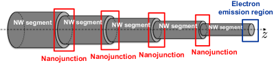
As illustrated in Fig. 1, we model a semiconductor nanotip as a sequence of decreasing diameter co-axial cylindrical NW segments. The length of each segment is assumed to be much longer than the electron mean free path. This allows us to model the incoherent electron transport in each segment using semiclassical MC methods accounting for the electron-phonon scattering. The NW segments are separated by the nanojunctions each assumed to have a length scale smaller than the electron mean free path allowing us to neglect the electron-phonon scattering. Therefore, a coherent electron scattering occurs at each nanojunction due to the NW diameter mismatch. We also assume that the electron emission takes place only from the surface terminating the last NW segment. This assumption is valid provided the overlap cross section of adjacent NW segments is much larger than the cross section area exposed to the vacuum preventing low energy electron emission at the nanojunctions. Such an assumption limits our model application to high aspect ratio nanotips.
Accordingly in Sec. II, a transfer matrix approach is utilized to derive the transmission and reflection coefficients (i.e., the probabilities) for the electron scattering at a nanojunction and electron emission from the surface terminating the nanotip. A numerical analysis of these quantities for the diamond based stand along nanojunction and a stand along emission region are provided in Sec. III. Sec. IV reports the results of the MC electron transport simulations for a minimal (two-segment) model of a diamond nanotip in the presence of an external electric field. The simulations incorporate the nanojunction electron scattering and electron emission from the surface terminating the nanotip. Sec. V provides concluding remarks.
II Theory of nanojunction scattering and nanotip emission
Let us consider a NW segment, , whose symmetry axis is aligned with -direction. An electron wave function in this segment is represented as a plane wave propagating in the -direction within a subband designated by a set of discrete quantum numbers
| (1) |
Here, the electron wavevector is
| (2) |
where is the total electron energy evaluated with respect to the bottom of the bulk conduction band. and are the longitudinal (-direction) and the transverse (radial direction) effective masses, respectively.
The transverse quantization of the wave vector, , arises from the radial component of the envelope wave function represented in cylindrical coordinates, , using Bessel functions of the first kind
| (3) |
Here, the normalization prefactor is with being the radius of NW segment . Assuming infinite confinement potential on the NW surface, roots of the Bessel function , define values of the quantized radial wave vector and a set of quantum numbers where is the angular momentum quantum number and is the radial quantum number.
II.1 Nanojunction scattering model
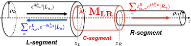
As illustrated in Fig. 2, we consider an incident electron wave in the -segment of radius entering a narrower () segment . This wave further passes to a narrower segment of radius and partially reflects back to segment . It is assumed that the length of the -segment is where is electron mean free path allowing us to neglect a phonon assisted scattering. The finite size of the -segment allows us to account for the quantum interference between the incident and reflected electron waves.
At the boundary of segment , the electron wave function, , is a superposition of the incident electron wave in an subband and the electron waves reflected to subbands designated by index each with an amplitude . At the -segment boundary, the electron wavefunction describing transmitted electron states is a superposition of the electron waves transmitted into subbands described by each with an amplitudes . These wavefunctions read
| (4) | |||||
| (5) |
where and satisfy Eq. (3) with , is the Kronecker delta, and the wave vectors in the exponents are given by Eq. (2).
As outlined in Appendix A, we match the boundary conditions for the wave functions and with the electron wave function in segment . This results in the following block-matrix equation for the reflection and transmission amplitudes
| (10) |
The column on the left-hand side is a vector with the upper Kronecker -block, , and the lower reflection amplitude, , block. The column on the right-hand side is formed from the vector and a column of zeros, , of the same size as . Each and index runs within the range of subbands participating in the scattering.
The transfer matrix in Eq. (10) contains four blocks. According to Appendix A, the block can be evaluated from the following block matrix product
| (11) |
Here, the -segment transfer matrix blocks are , , and with given by Eq. (2) with . Blocks of the matrices on the right and on the left contain , , , and with the electron wavevector components defined in Eq. (2). Blocks and are constructed from the radial envelope wave function overlap integrals in which defines radial eigenstates of segment .
According to the definition of the radial envelope function (Eq. (3)), an overlap integral between two adjacent segments and is
The integral vanishes for different angular momentum states (), reflecting angular momentum conservation due to the nanojunction axial symmetry. As a result, we consider only the scattering processes between subbands that have common quantum number but various radial numbers and .
Equation (10) can be viewed as two independent sets of linear equations, and . Their formal solution using matrix inversion provides the following simple representation for the transmission and reflection amplitudes in terms of the -segment transfer matrix blocks
| (13) | |||||
| (14) |
Using transmission and reflection amplitudes, we further introduce the transmission and reflection coefficients
| (15) | |||||
| (16) |
respectively. They give us probabilities for the electron transmission and reflection by segment and satisfy the identity
| (17) |
expressing conservation of the quantum mechanical probability current.
Finally, we define expressions for the reflection and transmission coefficients describing scattering of the incident electron in a subband of -segment to -segment and reflection back to segment . In this case, the calculation of associated transmission, , and reflection, , amplitudes should be performed according to Eqs. (13) and (14) where all superscripts and are swapped, i.e., . The transfer matrix should be evaluated according to Eq. (11) with including the transfer matrix argument. The transmission, , and reflection, , coefficients should be evaluated using Eqs. (15) and (16) with . The current conservation condition given by Eq. (17)with should satisfy as well.
II.2 Nanotip emission model
As illustrated in Fig. 3, an electron emission is considered in the positive -direction via the NW emission region extending between and . The model assumes that for the surface potential is , radial confinement potential at the NW surface is infinite, and the electron effective mass is anisotropic having transverse and longitudinal components. Accordingly, the radial component of the electron envelope wave function is given by Eq. (3) where for the sake of simplicity the segment index is dropped and the angular and radial quantum numbers are determined as the roots of with being the NW radius.
Once the electron crosses , its longitudinal effective mass changes abruptly to the vacuum electron mass, , and the surface potential becomes subsequently decreasing with (Fig. 3) until reaching zero at . Such a potential decrease can be associated with an external electric field applied in -direction. While the electric field lowers the surface potential , it is reasonable to assume that it has no effect on the radial confinement potential at the interval and keep it infinite. Such an assumption allows us to describe the electron envelope wave function using Eq. (3) with the set of quantum numbers at the interval . The confinement potential can further be set to zero at some point and electron diffraction outside this region introduced.
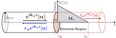
To find electron emission probability, the scattering theory approach is applied. The NW electron wave function at the entrence to the emission region, , is a superposition of the incident and reflected plane electron waves. Each wave is weighted with the confined radial state satisfying Eq. (3). The electron wave function exiting the emission region at is also a plane wave weighted with the same envelope wave function due to the presence of the radial confinement potential. Accordingly,
| (18) | |||||
| (19) |
with and being the emission region reflection and transmission amplitudes, respectively. The longitudinal electron wavevector, , is given by Eq. (2) with the superscript dropped for the sake of simpilisity. The emitted electron longitudinal wavevector reads
| (20) |
Notice that Eq. (20) depends on the electron mass in vacuum, , and the total electron energy, . Since the energy is conserved during the scattering process, it can be evaluated from Eq. (2) as
| (21) |
Appendix B outlines some details on matching the boundary conditions at and for the wavefunctions in Eqs. (18) and (19) using the transfer matrix formalism. This calculation results in the following matrix equation
| (26) |
for the reflection and transmission amplitudes at and , respectively. The transfer matrix describing the emission region is
| (27) |
and depends on the transfer matrix
| (28) |
associated with the surface potential . Here, the matrix product runs over small intervals along -direction numerated by index . Within each of these intervals, the surface potential is approximated by a rectangular potential barrier of a height . The longitudinal momentum entering Eq. (28) is
| (29) |
with the total energy provided in Eq. (21).
Solving Eq. (26) for the transmission and reflection amplitudes
| (30) | |||||
| (31) |
we further introduce the transmission and reflection coefficients
| (32) | |||||
| (33) |
describing electron emission and reflection probabilities. They satisfy the quantum mechanical current conservation condition
| (34) |
III Analysis of scattering and emission processes
This section presents numerical analysis of the electron scattering at a stand along nanojunction (Fig. 2) and the electron emission from a stand along NW segment (Fig. 3). The NWs are assumed to be made of diamond crystalline structures with the valley aligned along -direction. The nanojunction is set to have the radii nm, nm, and nm and the lengths of -segment nm. We further chose the radius of NW segment participating in the electron emission to be nm to set the stage for the simulations discussed in Sec. IV.
The effective mass in the -direction is identified as longitudinal and set to the bulk value . In the transverse direction, the effective mass is also set to its bulk value .Dimitrov et al. (2015) Notice that for the adopted radii of the NW segments, the anisotropy and nonparabolicity of the bulk conduction band can affect the values of the quantized subband effective masses.Neophytou et al. (2008) For the proof of principle calculations discussed below it is enough to use the bulk values. However, precise device modeling will require to account for the size quantization corrections to the bulk effective masses.
A convenient shorthand notation was introduced in Sec. II to denote a set of angular and radial quantum numbers that designate quantized electron subbands in NW segments. Below, specific values of these quantum numbers will be considered. Therefore, all expressions containing these quantities will show their explicit rather than the shorthand representation.
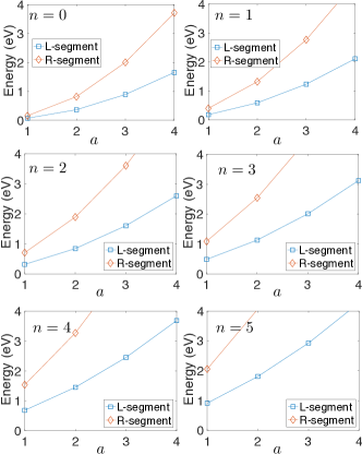
We start with Fig. 4 presenting calculated values of the quantized energy minima, , associated with conduction subbands of the and segments. The plot indicates a rapid (fractions of eV) growths of the energy values as the radial quantum number increases. The rapid growth is attributed to a small value, , of the transverse effective mass. Since , the energy values in segment are always larger than those in segment given the same quantum numbers and .
III.1 Nanojunction scattering
The transmission and reflection coefficients for the incident electron placed into a subband of either or segment given kinetic energy () are calculated using the formalism developed in Sec. II.1. Keeping in mind that the scattering conserves the angular momentum, we set for the transmitted and reflected electron states.
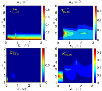
The calculated transmission coefficient (i.e., the probability), of an incident electron within and ( and ) subband of -segment to be scattered to subbands of -segment as a function of the kinetic energy is presented in the left (right) top panel of Fig. 5. Associated reflection coefficients are given in the lower row of Fig. 5. Provided an incident electron is in the subband , the left column of Fig. 5 indicates the following trends: For the electron kinetic energy within the range of meV, the electron gets reflected back into the state . Once the kinetic energy passes a threshold of meV an efficient transmission opens into the subband of segment . According to Fig. 4, the activation energy threshold can be identified as a gap between subband in segment and subband in segment . Thus, observed suppression of electron transmission below the energy threshold can be associated with the electron energy conservation.
The right panel in Fig. 5 describes the electron scattering from the subband . The activation energy gap for the transmission to subband of meV clearly shows up in the plot. Besides strong reflection back within the subband, a weak transmission to the subband of -segment is observed for meV. According to Fig. 4, the -subband is lower in energy than the -subband and, thus, does not have any activation threshold. Observed low values of the transmission coefficient are due to small values of associated overlap integral (Eq. (II.1)). The same explains lack of an efficient reflection to subband. Furthermore, vanishing overlap integrals between the subbands separated by larger energy gaps completely suppress the scattering to those bands as seen in Fig. 5 for ranging up to eV. Similar trends are observed for the transmission and reflection amplitudes of the incident electron placed into -segment as can be seen by comparing Figs. 5 and 6.
Finally, we point out that slow modulation of the transmission and reflection coefficients with increasing can be attributed to the effect of quantum interference associated with the finite size of segment . The electron wavelength scales as . Our estimate shows that the values of eV, 1.0 eV, and 3.0 eV corresponds to nm, 1.0 nm, and 0.6 nm, respectively. Taking into account that the length of the -segment is set to 0.5 nm, the variation of the kinetic energy in the range from 0 eV to 1.0 eV results in the electron wavelength values exceeding the region size and making the interference effect negligible. The variation of energy kinetic between 1 eV and 3 eV results in the wave length changes from twice to single C-segment length. In this case a slow modulation of the transmission and reflection probabilities occurs as observed in the plot.

To summarize, our analysis shows that, for the adopted parameters, efficient transmission through the NW junction occurs between subbands which are very close in energy. An efficient reflection typically happens for small values of kinetic energy. For electron kinetic energy of hundreds meV and below, the quantum interference has weak effect on the transmission and reflection coefficients provided the size of the interference region is about the electron mean free path. The quantum interference becomes important if eV.
III.2 Nanotip emission
Using the formalism developed in Sec. II.2, we model electron emission from the NW segment terminating a nanotip. The surface potential is adopted to have the form
| (35) |
for with being the electron affinity and being the amplitude of an external electric field applied along -axis. For the diamond surface terminating the NW at we set eV.Dimitrov et al. (2015) The external electric field values are varied within the range of MeV to 20 MeV. For these values, the length of the emission region, , varies between 60 nm and 15 nm, respectively.
Left column of Fig. 7 shows calculated transmission coefficients for the electron emission from subbands characterized by the angular quantum number and the radial quantum numbers . In the case of , the curves pick up fast oscillatory behavior around eV indicating that the electron experiences scattering at the very top of the potential barrier. Taking into account that the electron affinity is eV, a source of the energy shift eV allowing the electron to clear the surface potential barrier needs clarification.
The energy dependance of transmission (Eq. (32)) and reflection (Eq. (33)) coefficients within the emission region is determined by transfer matrix in the form of Eqs. (27)–(28) that depends on the electron wavevector, , given by Eq. (29). Taking into account that the energy is conserved during the emission, we substitute Eq. (21) into Eq. (29). This results in
| (36) |
where denotes the incident electron kinetic energy within subband, is the surface potential value at specified coordinate, and
| (37) |
is the energy shift due to the quantized band energy resulting from the electron mass mismatch at the interface. The effect of the effective mass mismatch has already been examined for the bulk-vacuum interface in relation with the transverse momentum conservation.Dimitrov et al. (2015) Below, we examine new consequences of this effect rising fomr the band quantization.
If the wave vector (Eq. (36)) is imaginary, the electron tunnels under the barrier. Once it becomes real, the electron clears top of the barrier and the transmission coefficient acquires an oscillatory behavior. According to Eq. (36), either real or imaginary value of the wavevector depends on whether the incident electron kinetic energy, , is larger or smaller than the effective potential energy barrier . According to Eq. (37), the contribution of to the effective potential can be zero if . If or then acquires either positive sign (decreasing the potential barrier) or negative sign (increasing the potential barrier).
In the adopted case of diamond NW, resulting in positive values of . Specifically, =0.1 eV shifts the emission energy threshold to meV as observed in Fig. 7 for . For the case of , the quantized energy contribution is even higher, eV, further shifting the barrier crossing threshold to meV. The values of eV and eV exceed the electron affinity, eV resulting in the fast oscillatory rise of the and starting at as clearly seen in the lower panels of Fig. 7.
IV Electron transport and emission simulations
In this section, we discuss the results of our electron transport and emission simulations performed for a minimal nanotip model. Following generic representation of a nanotip in Fig. 1, we narrow down the model to two NW segments, namely and connected via a single nanojunction. Adopted and NW segment radii are defined in Sec. III as nm and nm, respectively. The length of each segment is set to nm, where () is the coordinate of the left (right) end of () NW segment. In our minimal model, the electrons are emitted from the right end of segment characterized by coordinate .
To perform electron transport simulations, a bulk MC device simulation codeVasileska and Goodnick (2010) was modified to run 1D trajectories within quantized subbands. Following Ref. [Ramayya et al., 2008], we implemented a model for electron scattering by the acoustic and optical phonons in NWs. This model along with the bulk electron-phonon scattering model is briefly summarized in Appendix C. In all simulations discussed below, electrons with the kinetic energy satisfying the Boltzmann distribution at temperature of 300 K are injected into a single subband at the left end of segment (at ). An external electric field = 20 MV/m is applied along -axis. The field value is set larger than a typical field applied in an experiment to partially account for the geometric field enhancement effect. Since we focus on the quantum-size effects, the space charge effect is not included in the simulations. Using bulk value of the diamond DC dielectric constant , the field inside is estimated to be MV/m. Trajectory run time is chosen such that all electrons are either emitted or reflected back to the injection point.
Electron quantum scattering at the - junction and the electron emission and reflection at are accounted for via transmission and reflection coefficients introduced above with the same parameters as used in Sec. III. An electron reaching the - nanojunction during the MC simulation can cross the junction during a free-flight step. In this case, the transmission and reflection probabilities are cumulated and renormalized for all possible scatterings across the junction into various outgoing quantum states. A random number is generated and compared to the range of the cumulated probability corresponding to each possible scattering selecting the outgoing quantum states. The electron is then either transmitted or reflected, i.e., placed either at or coordinate depending on the scattering direction. Its kinetic energy is updated to conserve the total energy. For the case of electron emission and reflection at the right end of -segment, the similar algorithm is applied.
IV.1 Transport without electron-phonon scattering
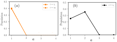
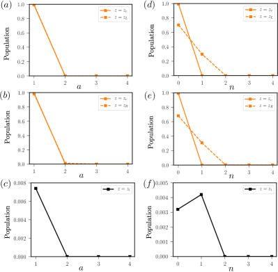
To clarify the effect of the nanojunction and the emission region scattering, results of the simulations performed with the phonon scattering turned off are discussed first. The electrons are initially injected into the and subband whose bottom energy eV (Fig. 4). Subsequently, ps trajectories are run and the electron population and energy distributions are recorded at different sampling points.
The subband population distribution normalized per total number of injected electrons sampled at the exits of the nanojunction, , and the emission region, , as well as at the injection coordinate, , are given in Fig. 8. Remember that the angular momentum conservation during the scattering processes preserves the quantum number . Panel (a) shows that during the course of simulation % of injected electrons (dashed line) are transmitted through the junction into a single , subband of NW segment and subsequently emitted to vacuum. According to panel (b), electrons reflected back to the injection point, , populate the subbands . This observation is in agreement with the discussion in Sec. III identifying that the junction scattering occurs within a narrow subband distribution.
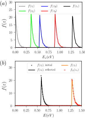
Distributions of the kinetic energy, , for the forward moving electrons at different points of the nanotip are shown in Fig. 9 (a). Each distribution has the form of Boltzmann function and is energy upshifted from the initial distribution, . The shape of each distribution is preserved because of the vanishing dependance of the transmission coefficients on the energy within the distribution width and lack of the electron-phonon scattering. The kinetic energy shift of eV between distributions at the injection point, , and the nanojunction entrance, , as well as between the point of the nanojunction exit, , and the emission region entrance, , reflects electrons acceleration by the external electric field.
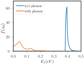
The kinetic energy difference of eV for the distributions describing electrons entering, , and exiting, , the --junction is the energy difference between the , subband in -segment and the , subband of -segment. For the electrons entering, , and exiting, , the emission region, the shift in the kinetic energy is determined by the momentum variation provided by Eqs. (20) and (21). Notice that the electron kinetic energy distribution at the entrance to the emission region, , (red) peaks eV which is above the potential barrier ( eV). Accordingly, all electrons entering the emission region clear the barrier as can be seen in Fig. 8a.
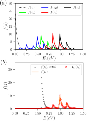
The total energy, , distributions for the electrons emitted to vacuum and reflected back are shown in Fig. 9 (b). Specifically, the energy distribution for all emitted electrons (solid orange line) is compared with the distribution of electrons emitted from , subband (orange crosses). The distributions coincide which is in agreement with Fig. 8 (a) showing that the emission occurs solely from , subband. Although the electrons scattered back are distributed between , subbands (Fig. 8 (b)), the coincidence between the total energy distribution for all electrons scattered back (solid black line) and their initial distribution (grey dots) in Fig. 9 (b) reflects conservation of the total energy (i.e., the absence of the dissipation processes). The upshift of eV between the emitted and injected/reflected energy distribution is due to the electron acceleration by the external electric field.
IV.2 Transport with electron-phonon scattering
Given the same, , , initial conditions, we now turn the electron-phonon scattering on and examine associated electron trajectories which were run on the timescale of ps. The normalized electron population distributions are presented in Fig. 10. Since the electron-phonon scattering processes do not conserve electron angular momentum, the population distributions are presented as functions of the radial and angular quantum numbers. Panels (a) and (d) clearly show that during the transport through -segment, the phonons cause population relaxation down to subbands , and , . According to panels (b) and (e), electron transmission through the nanojunction occurs to the same subbands. In particular is preserved due to the momentum conservation by the nanojunction scattering. While moving through -segment, electrons further relax to the lowest energy band (, ) and % of the injected electrons get emitted. According to panels (c) and (f) only % of the electrons are reflected back to the injection point by the nanojunction.
Comparison of the kinetic and the total energy distributions in the case of phonon scattering turned off (Fig. 9) and on (Fig. 11), reveals that the latter distribution functions are significantly broadened due to the inter- and intraband population transfer already identified in Fig. 10. The side peaks appear as the phonon replicas of the main distribution peaks shifted up and down for the energy of the optical phonon quantum. In Fig. 11 (b), the coincidence between the energy distribution function of the electrons emitted from the subband , , , with the distribution of all electrons emitted by the nanotip, , is also in agreement with Fig. 10, confirming that the emission occurs from the lowest energy band. Notice that, in Fig. 11 (a), the kinetic energy of the electrons entering the emission region, , (red) is distributed above eV. This is above the electron affinity level ( eV) and according to Fig. 7 results in transmission probability one.
IV.3 Comparison of nanotip and bulk emission
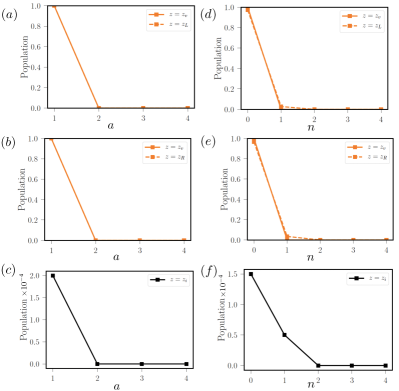
To compare the nanotip electron transport and emission properties with those in bulk diamond, we injected the electrons into the lowest energy subband (, ) of the nanotip. Furthermore, a bulk slab of equivalent, 200 nm, thickness and equivalent crystallographic axes orientation was considered. Electrons were injected at one side of the slab to the bottom of [100] valley forming the same Maxwell distribution as in the case of the nanotip and further accelerated by the same external electric field. The MC device simulation codeVasileska and Goodnick (2010) was used without any modifications adopting a bulk phonon scattering model summarized in Appendix C. The emission from the slab was modeled using the same potential as for the nanotip. In both cases the electron trajectories were run for ps.
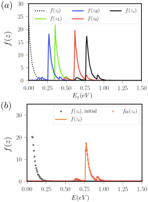
According to Fig. 12 (a), (b), (d), and (e), the electron transport is confined to the lowest energy subband of both and NW segments. About 100% of the injected electrons are emitted. According to panels (c) and (f) of the same figure, a negligible amount, 0.02%, of the injected electrons is reflected back. The energy distributions in Fig. 13 are weakly influenced by the phonon assisted scattering. The phonon assisted scattering rate in a NW depends on the density of final states that scales as representing the van Hove singularity [Eqs. (C) and (C)]. denotes kinetic energy of the scattered electrons. Accordingly, the sharply peaked density of states allows the scattering only between or near the bottoms of the subbands. In our case, the interband scattering is suppressed, since electrons do not gain enough kinetic energy to be scattered to the higher energy subbands. Observed high emission rate has the same origin as in the case of Sec. IV.2.
In the case of bulk, 100% of electrons reach the emission region but only 21% of them are emitted. This effect can be rationalized by looking at the kinetic energy distribution of the electrons, , reaching the emission region presented in Fig. 14. According to the plot, the phonon assisted scattering has profound effect on the transport by reducing the electron energy to the range below eV. This is below the electron affinity value of 0.3 eV. Thus, the electrons have to tunnel under the barrier to escape to the vacuum which significantly lowers the emission rate. Compared to the nanotip case, high phonon scattering rate originates from the scaling of the scattered electron density of states which is [Eqs. (C) and (C)]. In contrast to the sharply peaked van Hove singularity in NWs, bulk square root dependance allows for a broad range of states accessible by the scattered electrons.
V Concluding remarks
We have developed a theory addressing electron scattering by diameter variation in a semiconductor nanotip and electron emission from the surface terminating the nanotip. The theory is applied to examine transmission and reflection probabilities for the varying diameter nanojunction and for the emission region of a diamond nanotip. The analysis shows that the nanojunction scattering occurs within a narrow range of quantized conduction electron subbands due to the fast decrease of the envelope function overlap. As further demonstrated, the mismatch in the NW transverse effective mass and electron mass in vacuum within the emission region along with the band energy quantization can result in a substantial lowering of the emission potential and the enhancement of the electron emission from the nanotip. Noteworthy that the emission surface passivation should affect the emission properties. Such effects cannot be accounted directly in the effective mass approximation and are subject of separate studies utilizing, e.g., atomistic surface modeling. Atomistic modeling of the emission region can also be employed to validate adopted distribution of the confinement and the emission surface potentials (Fig. 3) and make necessary model refinements. Ultimate validation of the proposed emission model requires comparison with experimental measurements.
The scattering and emission models have been implemented into the MC transport simulations and used to simulate the transport and emission properties of a minimal geometry nanotip. The simulations show that the interplay of the electron-phonon scattering and the quantum size effects can result in up to 100% emission of the injected electrons. In contrast, the phonon assisted scattering in an equivalent size and orientation bulk slab of diamond leads to a significantly lower emission outcome. This emphasizes an advantage of nanostructuring to achieve an efficient electron source. Noteworthy, that the nanotip surface roughness and electron-impurity scattering effects are not accounted for in the model. Such effects can potentially lower desired electron emission efficiency and require further examination. Although the simulations are performed for the case of a diamond based nanostructure, our model is general and can be parametrized to study the same effects in nanotips of various semiconductor materials, e.g., GaAs. Finally, the methodology sets the stage for investigation of the field and/or photoemission dynamics in semiconductor nanotips subject to implementation of specific electron injection or photoexcitation models.
Acknowledgements.
This work is supported by the Laboratory Research and Development (LDRD) program at Los Alamos National Laboratory. A. P. would like to acknowledge David H. Dunlop for stimulating discussions of the scattering and emission models. We would like to thank Evgenya I. Simakov and Bo Kyoung Choi for comments on the manuscript. Author contributions: A.P., C.H., T.J.T.K. conceived and developed the core ideas. A.P. developed and implemented the nanoscale scattering models. C.H. implemented and performed the MC transport and emission simulations. All authors took part in the result analysis. A.P. and C.H. wrote this manuscript.Appendix A Derivation of transfer matrix
Conduction band electron wavefunction in the -segment is defined as
| (38) |
where is a superposition of counter propagating electron waves characterized by the wavevectors both defined by Eq. (2). The envelope wavefunction associated with the ket is given by Eq. (3).
For a single subband , the wave function and its derivative, , at coordinates and (Fig. 2) are related via the following transfer matrix relationEconomou (2006)
| (43) |
Now, we introduce a column vector of the wave functions and their derivatives with . In these notations, we recast Eq. (43) to the block matrix form
| (48) |
where the diagonal transfer matrix block is . The upper and lower off-diagonal blocks are and , respectively.
Matching the boundary conditions for the -segment wave function (Eq. (4)) and its derivative with the -segment wave function (Eq. (38)) and its derivative, we get
| (49) | |||||
| (50) |
Here, the overlap integrals and are defined in Eq. (II.1). Further defining a column vectors of the Kronecker deltas, , and a column of reflection amplitudes, , with , we recast Eqs. (49) and (50) to an equivalent block-matrix form that reads
| (53) | |||||
| (56) |
In Eq. (53), the overlap integral blocks are , the unit matrix is , the wavevector matrix is , and the exponent of the wavevector matrix is . All .
Similar to above, matching the boundary conditions at the - interface for the wavefunctions defined in Eqs. (38) and (5) and their derivatives, results in
| (57) | |||||
| (58) |
This set of linear equations is equivalent to the block-matrix equation
| (61) | |||||
| (64) |
where and are the same size columns of transmission amplitudes and zeros, respectively. The overlap integral matrix is and is a matrix of zeros. and . All the matrices are of the size.
Appendix B Derivation of transfer matrix for electron emission
As demonstrated in Sec. II.2 electron emission does not mix electron states that belong to different subbands. Therefore, we describe this process using transfer matrix representation associated with a single subband denoted by .
Let us define the electron wave function within the emission region as
| (65) |
with the ket satisfying Eq. (3). Values of the wavefunction and its derivative at the boundaries of the emission region are determined by the following equation
| (70) |
with the transfer matrix defined in Eq. (28).Economou (2006)
Matching the boundary conditions for the electron wavefunctions given by Eqs. (18) and (65) and their derivatives at can be performed in analogy with Eqs. (49)–(53). This results in
| (73) | |||||
| (76) |
where , is given by Eq. (2) and the ratio account for the electron mass mismatch at the interface.
Appendix C Models for electron scattering by acoustic and optical phonons
This Appendix provides a summary of the models for the electron-phonon scattering in bulk crystalline and NW structures that were implemented into the MC transport simulations discussed in Sec. IV.
In bulk diamond crystals, the acoustic phonons cause electron scattering within a conduction band valley with the rate
where is the total energy of a conduction electron, is the band non-parabolicity parameter, is crystal density, is the sound velocity, and is the acoustic deformation potential.
The intervalley electron scattering in the bulk diamond is facilitated by the optical phonons and characterized by the following rate
where is the total initial energy of a conduction band electron, is its final energy with being the energy difference between the bottoms of initial and final valleys, is a quantum of phonon energy, and is the number of equivalent final valleys. The phonons population at thermal equilibrium is .
In the case of NW structures, we define a set of quantum numbers designating an electron subband (see Sec. II) in which its kinetic energy is . The rate for this electron to scatter into subband due to the interaction with the acoustic phonons is(Ramayya et al., 2008)
Here, the electron final state kinetic energy is
| (85) |
with set specifically for the acoustic phonons. Due to the presence of van Hove singularity in 1D density of electron states one requires that as ensured by the Heaviside step function, , entering Eq. (C). The overlap integral in Eq. (C) defined in terms of the normalized Bessel functions of the first kind (Eq. (3)) reads
| (86) |
Notice that in contrast to Eq. (II.1), this integral does not conserve the angular momentum quantum number and has dimensionality of the inverse area.
References
- Choi et al. (1999) W. Choi, D. Chung, J. Kang, H. Kim, Y. Jin, I. Han, Y. Lee, J. Jung, N. Lee, G. Park, et al., Appl. Phys. Lett. 75, 3129 (1999).
- Wang et al. (2001) Q. Wang, M. Yan, and R. Chang, Appl. Phys. Lett. 78, 1294 (2001).
- Chandrasekhar (2018) P. Chandrasekhar, in Conducting Polymers, Fundamentals and Applications (Springer, Cham, Switzerland, 2018) pp. 73–75.
- Posada et al. (2014) C. M. Posada, E. J. Grant, R. Divan, A. V. Sumant, D. Rosenmann, L. Stan, H. K. Lee, and C. H. Castano, J. Appl. Phys. 115, 134506 (2014).
- Teo et al. (2005) K. B. Teo, E. Minoux, L. Hudanski, F. Peauger, J.-P. Schnell, L. Gangloff, P. Legagneux, D. Dieumegard, G. A. Amaratunga, and W. I. Milne, Nature 437, 968 (2005).
- Li et al. (2013) X. Li, M. Li, L. Dan, Y. Liu, and C. Tang, Phys. Rev. ST Accel. Beams 16, 123401 (2013).
- Baryshev et al. (2014) S. V. Baryshev, S. Antipov, J. Shao, C. Jing, K. J. Pérez Quintero, J. Qiu, W. Liu, W. Gai, A. D. Kanareykin, and A. V. Sumant, Appl. Phys. Lett. 105, 203505 (2014).
- Adamo et al. (2009) G. Adamo, K. F. MacDonald, Y. Fu, C. Wang, D. Tsai, F. G. de Abajo, and N. Zheludev, Phys. Rev. Lett. 103, 113901 (2009).
- Peralta et al. (2013) E. Peralta, K. Soong, R. England, E. Colby, Z. Wu, B. Montazeri, C. McGuinness, J. McNeur, K. Leedle, D. Walz, et al., Nature 503, 91 (2013).
- Wong et al. (2015) L. J. Wong, I. Kaminer, O. Ilic, J. D. Joannopoulos, and M. Soljačić, Nat. Photonics 10, 46 EP (2015).
- Zhao et al. (2018) Z. Zhao, T. W. Hughes, S. Tan, H. Deng, N. Sapra, R. J. England, J. Vuckovic, J. S. Harris, R. L. Byer, and S. Fan, Opt. Espress 26, 22801 (2018).
- Bocharov and Eletskii (2013) G. S. Bocharov and A. V. Eletskii, Nanomaterials 3, 393 (2013).
- De Heer et al. (1995) W. A. De Heer, A. Chatelain, and D. Ugarte, Science 270, 1179 (1995).
- Maiti et al. (2001) A. Maiti, J. Andzelm, N. Tanpipat, and P. von Allmen, Phys. Rev. Lett. 87, 155502 (2001).
- Di Bartolomeo et al. (2016) A. Di Bartolomeo, M. Passacantando, G. Niu, V. Schlykow, G. Lupina, F. Giubileo, and T. Schroeder, Nanotechnology 27, 485707 (2016).
- Zhi et al. (2005) C. Zhi, X. Bai, and E. Wang, Appl. Phys. Lett. 86, 213108 (2005).
- Giubileo et al. (2017) F. Giubileo, A. Di Bartolomeo, L. Iemmo, G. Luongo, M. Passacantando, E. Koivusalo, T. Hakkarainen, and M. Guina, Nanomaterials 7, 275 (2017).
- Wu et al. (2009) Z.-S. Wu, S. Pei, W. Ren, D. Tang, L. Gao, B. Liu, F. Li, C. Liu, and H.-M. Cheng, Adv. Mater. 21, 1756 (2009).
- Shao and Khursheed (2018) X. Shao and A. Khursheed, Appl. Sci 8, 868 (2018).
- Okano et al. (1996) K. Okano, S. Koizumi, S. R. P. Silva, and G. A. Amaratunga, Nature 381, 140 (1996).
- Yamaguchi et al. (2009) H. Yamaguchi, T. Masuzawa, S. Nozue, Y. Kudo, I. Saito, J. Koe, M. Kudo, T. Yamada, Y. Takakuwa, and K. Okano, Phys. Rev. B 80, 165321 (2009).
- Terranova et al. (2015) M. L. Terranova, S. Orlanducci, M. Rossi, and E. Tamburri, Nanoscale 7, 5094 (2015).
- Biswas (2018) D. Biswas, Phys. Plasmas 25, 043105 (2018).
- Jarvis et al. (2010) J. D. Jarvis, H. Andrews, B. Ivanov, C. Stewart, N. De Jonge, E. Heeres, W.-P. Kang, Y.-M. Wong, J. Davidson, and C. Brau, J. Appl. Phys. 108, 094322 (2010).
- Ben-Zvi et al. (2004) I. Ben-Zvi, X. Chang, P. D. Johnson, Kewisch, and T. S. Jörg; Rao (Brookhaven National Laboratory, Upton, NY, 2004).
- Wang et al. (2011a) E. Wang, I. Ben-Zvi, T. Rao, D. A. Dimitrov, X. Chang, Q. Wu, and T. Xin, Phys. Rev. ST Accel. Beams 14, 111301 (2011a).
- Wang et al. (2011b) E. Wang, I. Ben-Zvi, X. Chang, Q. Wu, T. Rao, J. Smedley, J. Kewisch, and T. Xin, Phys. Rev. ST Accel. Beams 14, 061302 (2011b).
- Dimitrov et al. (2010) D. Dimitrov, R. Busby, J. Cary, I. Ben-Zvi, T. Rao, J. Smedley, X. Chang, J. Keister, Q. Wu, and E. Muller, J Appl. Phys. 108, 073712 (2010).
- Dimitrov et al. (2015) D. Dimitrov, D. Smithe, J. Cary, I. Ben-Zvi, T. Rao, J. Smedley, and E. Wang, J. Appl. Phys. 117, 055708 (2015).
- Dowell et al. (2010) D. Dowell, I. Bazarov, B. Dunham, K. Harkay, C. Hernandez-Garcia, R. Legg, H. Padmore, T. Rao, J. Smedley, and W. Wan, Nucl. Instrum. Methods Phys. Res. A 622, 685 (2010).
- Spicer (1977) W. Spicer, Appl. Phys. A 12, 115 (1977).
- Karkare et al. (2013) S. Karkare, D. Dimitrov, W. Schaff, L. Cultrera, A. Bartnik, X. Liu, E. Sawyer, T. Esposito, and I. Bazarov, J. Appl. Phys. 113, 104904 (2013).
- Karkare et al. (2015) S. Karkare, D. Dimitrov, W. Schaff, L. Cultrera, A. Bartnik, X. Liu, E. Sawyer, T. Esposito, and I. Bazarov, J. Appl. Phys. 117, 109901 (2015).
- Karkare et al. (2014) S. Karkare, L. Boulet, L. Cultrera, B. Dunham, X. Liu, W. Schaff, and I. Bazarov, Phys. Rev. Lett. 112, 097601 (2014).
- Neophytou et al. (2008) N. Neophytou, A. Paul, M. S. Lundstrom, and G. Klimeck, IEEE Trans. Electron Devices 55, 1286 (2008).
- Vasileska and Goodnick (2010) D. Vasileska and S. M. Goodnick, “Bulk monte carlo: Implementation details and source codes download,” (2010), https://nanohub.org/resources/9109 .
- Ramayya et al. (2008) E. Ramayya, D. Vasileska, S. Goodnick, and I. Knezevic, J. Appl. Phys. 104, 063711 (2008).
- Economou (2006) E. N. Economou, Green’s Functins in Quantum Physics (Springer, New York, 2006).
- Nava et al. (1980) F. Nava, C. Canali, C. Jacoboni, L. Reggiani, and S. Kozlov, Solid State Commun. 33, 475 (1980).
- Jacoboni and Reggiani (1983) C. Jacoboni and L. Reggiani, Rev. Mod. Phys. 55, 645 (1983).