Designing Metagratings Via Local Periodic Approximation:
From Microwaves to Infrared
Abstract
Recently, metamaterials-inspired diffraction gratings (or metagratings) have demonstrated unprecedented efficiency in wavefront manipulation by means of relatively simple structures. Conventional one-dimensional (1D) gratings have a profile modulation in one direction and a translation symmetry in the other. In 1D metagratings, the translation invariant direction is engineered at a subwavelength scale what allows one to accurately control polarization line currents and, consequently, the scattering pattern. In bright contrast to metasurfaces, metagratings cannot be described by means of surface impedance densities (or local reflection and transmission coefficients). In this paper, we present a simulation-based design approach to construct metagratings in the “unit cell by unit cell” manner. It represents an analog of the local periodic approximation (LPA) that has been used to design space modulated metasurfaces and allows one to overcome the limitations of straightforward numerical optimization and semi-analytical procedures that have been used up to date to design metagratings. Electric and magnetic metagrating structures responding to respectively transverse electric (TE) and transverse magnetic (TM) incident plane-waves are presented to validate the proposed design approach.
I introduction
In the last decade there has been tremendous interests in metasurfaces due to their amazing capabilities in manipulating electromagnetic fields Kildishev et al. (2013); Glybovski et al. (2016); Asadchy et al. (2018) and broad range of potential applications Yu and Capasso (2014); Chen et al. (2016); Asadchy et al. (2018); Capasso (2018). Metasurfaces are represented by dense distributions of engineered subwavelength scatterers on a surface being planar analogs of metamaterials. When the characteristics of a metasurface are spatially modulated, it can perform wavefront transformations Yu et al. (2011); Pfeiffer and Grbic (2013). The local periodic approximation (LPA) plays a crucial role in designing such metasurfaces and has been already used for long time Pozar et al. (1997); Epstein and Eleftheriades (2016). Essentially, it serves to estimate scattering properties of a unit cell embedded in a nonuniform array. To that end, a unit cell is placed in the corresponding uniform array whose reflection and transmission coefficients are then attributed to the unit cell in a nonuniform array. Scattering parameters of a uniform array are usually calculated from full-wave numerical simulations. However, there are particularly simple cases (e.g. metallic patches) that can be treated analytically Luukkonen et al. (2008); Wang et al. (2018).
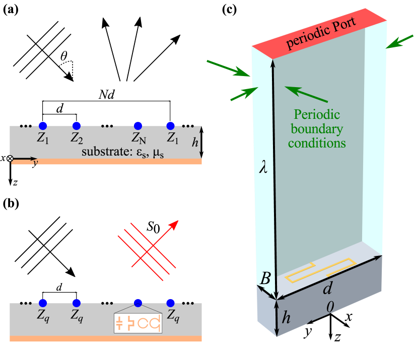
Recently, metamaterials-inspired diffraction gratings have demonstrated unprecedented efficiency in manipulating scattering patterns with relatively simple structures Sell et al. (2017); Ra’di et al. (2017); Epstein and Rabinovich (2017); Popov et al. (2018); Chen et al. (2018); Popov et al. (2019). Reflecting configuration of a metagrating represented by a one-dimensional periodic array of thin “wires” placed on top of a metal-backed dielectric substrate is illustrated in Fig. 1 (a). Generally, each period of a metagrating consists of different “wires”. Noteworthy, the distance between adjacent “wires” always remains of the order of operating wavelength , which does not allow one to introduce neither averaged surface impedances nor local reflection coefficient in contrast to metasurfaces. Incident wave excites electric or magnetic polarization line currents in “wires” that can be controlled by judiciously adjusting the electromagnetic response of the “wires”. Consequently, it becomes possible to manipulate diffraction orders. It has been demonstrated that it is possible to achieve perfect nonspecular reflection and beam splitting with a single “wire” per period Ra’di et al. (2017); Epstein and Rabinovich (2017); Chen et al. (2018). In a more general manner, it was shown that in order to perfectly control diffraction patterns one needs two degrees of freedom (represented by reactively loaded “wires”) per each propagating diffraction order Popov et al. (2019). However, even having the number of reactive “wires” per period equal to the number of propagating diffraction orders enables to perform efficient multichannel reflection, as demonstrated in Popov et al. (2018).
Practically, a “wire” is constituted from subwavelength meta-atoms arranged in a dense uniform 1D array . Geometrical parameters of meta-atoms determine electromagnetic response of a “wire”. Up to date metagratings have been designed either by performing 3D full-wave numerical optimization of a whole metagrating’s period Ra’di et al. (2017) or semi-analytically Chalabi et al. (2017); Epstein and Rabinovich (2017); Rabinovich and Epstein (2018); Popov et al. (2018, 2019). While the first approach can be very time consuming when it comes to designing metagratings having many “wires” per period, the second one allows one to consider only very simple meta-atoms such as printed capacitors Epstein and Rabinovich (2017) or dielectric cylinders Chalabi et al. (2017). In this paper, we develop the local periodic approximation for designing metagratings with the help of 3D full-wave numerical simulations. In comparison to a straightforward numerical optimization, it significantly reduces the time spent on the design of metagratings since within the LPA one deals with a single unit cell at a time [meaning that we consider a uniform array formed by a given unit cell as illustrated by Fig. 1(b)]. Contrary to simple analytical models, the LPA also allows one to deal with complex meta-atom’s geometries and accurately account for interactions between adjacent “wires”.
The outline of the paper is as follows. In the second section we describe a retrieval technique which is used to extract characteristics of a “wire” from scattering parameters of the corresponding uniform array. We consider “wires” possessing either electric or magnetic responses which allows one to deal with both TE and TM polarizations. In the same section, we outline a model that can be used in a full-wave simulation software to construct a look-up table connecting retrieved characteristics of “wires” with corresponding parameters of meta-atoms. The third section is devoted to validation examples where we demonstrate metagratings’ designs operating in microwave and infrared frequency domains. In the fourth section we discuss remained challenges and conclude the paper.
II Local periodic approximation
for metagratings
We consider reflecting metagratings operating either under TE or TM incident wave polarization. Therefore, each “wire” composing a metagrating can be characterized by a scalar electric impedance density (or scalar magnetic admittance density in the case of a “wire” possessing magnetic response). However, the approach can be readily generalized to transmitting metagratings as it is discussed in the last section, polarization insensitive metagratings can be developed by designing “wires” having both electric and magnetic responses and applying the method developed further for each polarization separately. Previously, one has distinguished between load- and input-impedance densities Epstein and Rabinovich (2017); Popov et al. (2018, 2019) which we do not separate in the present study dealing only with impedance density as the principal characteristic of a “wire”. To be more accurate, we assume that the impedance density represents the sum of the load-impedance density and reactive part of the input-impedance density. According to the LPA, in order to find impedance density, a “wire” is placed in the corresponding uniform array (period ) illuminated by a plane-wave incident at angle as illustrated by Fig. 1 (b). We start by describing a way to retrieve electric impedance and magnetic admittance densities from scattering parameters. Since () represents itself as a complex number and an electric (magnetic) line current radiates TE (TM) wave, it is sufficient to measure only the complex amplitude of the specularly reflected TE (TM) plane-wave. Noteworthy, time dependence is assumed throughout the paper.
II.1 Electric response, TE polarization
An electric polarization line current (excited by TE plane-wave in a “wire” composing the uniform array) is linked to the complex amplitude of the electric field of the specularly reflected wave via the following formula (see Appendix A)
| (1) |
Here, and are the wavenumber and characteristic impedance outside the substrate, is the Fresnel’s reflection coefficient from the metal-backed substrate of a TE plane-wave at incidence angle and . Since all “wires” are assumed to be very thin, they are modeled as lines represented mathematically by the Dirac delta function . Consequently, the interaction with the substrate and between adjacent “wires” can be taken into consideration analytically by means of the mutual-impedance density (see Appendix A). It allows one to obtain the characteristic of a “wire” itself and not of the array. “Wire’s” electric impedance density is found by means of Ohm’s law leading to the following expression for
| (2) |
where represents the value of the external electric field (incident wave plus its reflection from the metal-backed substrate) at the the “wire” located at and . The radiation resistance of a “wire” is equal to being independent on its particular implementation as it follows from power conservation conditions Tretyakov (2003). It is important to note that mutual-impedance density depends only on the period of the uniform array and parameters of the metal-backed substrate, but does not depend on the current . It means that the impedance density given by Eq. (2) accurately represents the characteristic of the corresponding “wire” in a nonuniform array as long as the distance between adjacent “wires” and the metal-backed substrate remain the same as those of the uniform array. However, we leave open the questions of accuracy when considering “wires” built up from finite size meta-atoms as infinitely thin and estimating mutual interactions by means of analytically calculated mutual-impedance density.
II.2 Magnetic response, TM polarization
The case of TM polarization and “wires” possessing magnetic response can be treated with the help of duality relations Felsen and Marcuvitz (1994): , , and . Since the metal-backed dielectric substrate is not replaced by the corresponding dual equivalent, we have to additionally make the following substitution . Thus, from Eq. (1) one can arrive at the formula for retrieving the magnetic current from the complex amplitude of the magnetic field of the specularly reflected plane-wave (see Appendix B)
| (3) |
where is the Fresnel’s reflection coefficient from the metal-backed substrate of a TM-polarized plane-wave at incidence angle . As previously, the interaction with the substrate and between adjacent “wires” can be taken into account by means of the mutual-admittance density calculated analytically (see Appendix B). Then, the magnetic admittance density can be found as
| (4) |
Here is the value of the external magnetic field at the “wire” located at and , represents the radiation conductance.
II.3 Look-up table
As it is stated above, in practice a “wire” would be implemented with subwavelength meta-atoms arranged in a line. The ultimate goal of the developing approach is to construct a look-up table linking geometrical parameters of meta-atoms with corresponding impedance (admittance) densities. To that end, we harness 3D full-wave numerical simulations (in our examples COMSOL MULTIPHYSICS is used). Although, Eqs. (1)–(4) are obtained by modelling “wires” as infinitesimally thin, all practical features of unit cells (like dielectric and conduction losses, finite thickness of metallic traces, etc.) are taken into account by means of numerical simulations. The geometry of the model consists of two principal parts: a tested unit cell (illustrated by a printed inductance on a metal-backed dielectric substrate in Fig. 1 (c)) and air region. Periodic boundary conditions are imposed on the side faces (as shown in Fig. 1 (c)). The model is excited by a periodic port assigned to the face of the air region in opposite to the unit cell, as highlighted in red color in Fig. 1 (c). The periodic Port creates a plane-wave incident at angle . It is important to take into account since meta-atoms are usually spatially dispersive (impedance density depends on the incidence angle, see for instance Ref. Epstein and Eleftheriades (2016)). The thickness of the air region equals operating vacuum wavelength which is normally enough to eliminate higher order evanescent modes. The periodic port is also used as a listening port to calculate the scattering parameter . It is related to the complex amplitude in Eq. (1) as . In the case of TM polarization .
III examples
In order to validate the developed approach, we first employ it to construct look-up tables that are further used to implement metagratings for controlling propagating diffraction orders. In order to find impedance densities necessary to establish a given diffraction pattern we use the theoretical approach developed in Ref. Popov et al. (2018). In what follows, we focus on two frequency ranges: microwave (operating vacuum wavelength mm) and infrared (operating vacuum wavelength m).
III.1 Microwave frequency range
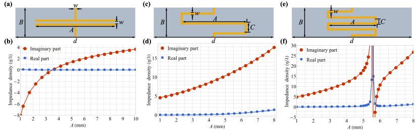
We start by considering simple meta-atoms represented by printed capacitance and inductance (illustrated in Fig. 2) that have already been used to implement metagratings at microwave frequencies by means of printed circuit board (PCB) technology Chen et al. (2018); Popov et al. (2019). In the simulations, we take into account practical aspects of the design such as finite thickness of the copper traces ( m) and dielectric losses introduced by the substrate (F4BM220 in our examples, with loss tangent ). Figure 2 depicts the impedance densities calculated by means of the developed LPA at GHz (vacuum wavelength is mm). It is seen that having printed capacitance and inductance one is able to cover a broad range of impedance densities (imaginary part) that is normally enough to realize any diffraction pattern for TE polarization. It is important to note, that “wires” can exhibit significant resistive response (see Fig. 2 (f) at the resonance) which should be kept in mind while designing metagratings. When comparing the numerical results with analytical models used in Refs. Epstein and Rabinovich (2017); Popov et al. (2019), one would see very good agreement for the imaginary part of the impedance density at small values of parameter . The resonance observed in Fig. 2 (f) appears when one decreases the parameter and it cannot be found by simple analytical formula used in Ref. Popov et al. (2019).
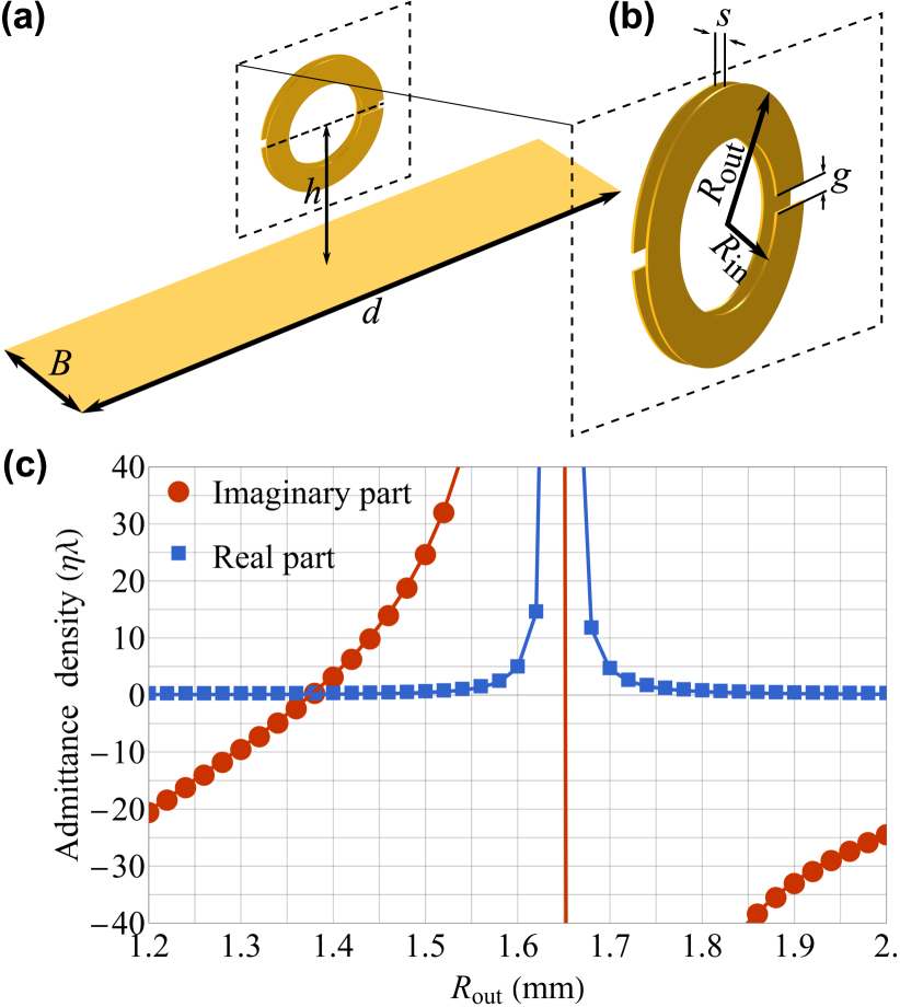
In order to deal with TM polarization, we harness split ring resonators (SRRs) excited by the magnetic field and, thus, having effective magnetic response. Figure 3 (a) illustrates the schematics of the unit cell which at close look consists of two SRRs separated by a short distance as seen from Fig. 3 (b). The unit cell has an inversion center allowing to eliminate the bianisotropic response attributed to single and double SRRs Marqués et al. (2002); Sauviac et al. (2004). In order to adjust the response of a “wire” represented by a 1D array of SRRs, we use the outer radius as a free parameter. The result of applying the LPA to find an equivalent admittance density is depicted in Fig. 3 (c). Due to the small separation distance between the two SRRs we are able to achieve strong magnetic response with the outer radius being of the order of . As in the case of TE polarization discussed above we see that when approaching the resonance there is an increase of the real part of the “wire’s” admittance density resulting in enhanced absorption.
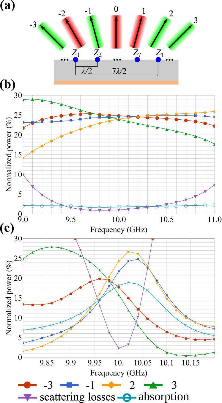
In order to validate calculated impedance and admittance densities we develop designs of metagratings based only on the data from Figs. 2 and 3 to construct a certain diffraction pattern. Particularly, we demonstrate a splitting of normally incident plane-wave equally between four propagating diffraction orders (-3, -1, +2 and +3) while suppressing the rest three (-2, 0 and +1), as illustrated by the schematic in Fig. 4 (a). In accordance with Ref. Popov et al. (2018), to that end we need the number of reactive “wires” per period equal to the number of propagating diffraction orders, i.e. seven. Although Ref. Popov et al. (2018) deals only with electric line currents and TE polarization, it is straightforward to generalize the approach to magnetic currents and TM polarization (See Appendix B). Figures 4 (b) and (c) demonstrate the frequency response of electric and magnetic metagratings designed for GHz. Overall, one can see that despite all practical limitations, the designed metagratings almost perfectly perform the desired splitting of the incident wave. It is important to note that the response of the metagrating operating under TE polarization (Fig. 4 (b)) shows a broader response than the one operating under TM polarization (Fig. 4 (c)). It is naturally explained by the resonant behavior of the considered SRR-based unit cell (see Fig. 3 (b)). Indeed, printed capacitance and inductance (illustrated, respectively, by Figs. 2 (a) and (c)) used for the metagrating dealing with TE polarization do not exhibit resonances (see Figs. 2 (b) and (d)). The other feature of the magnetic metagrating is the significant absorption (compared to the case of TE polarization) which, however, does not deteriorate the overall performance.
III.2 Infrared frequency range
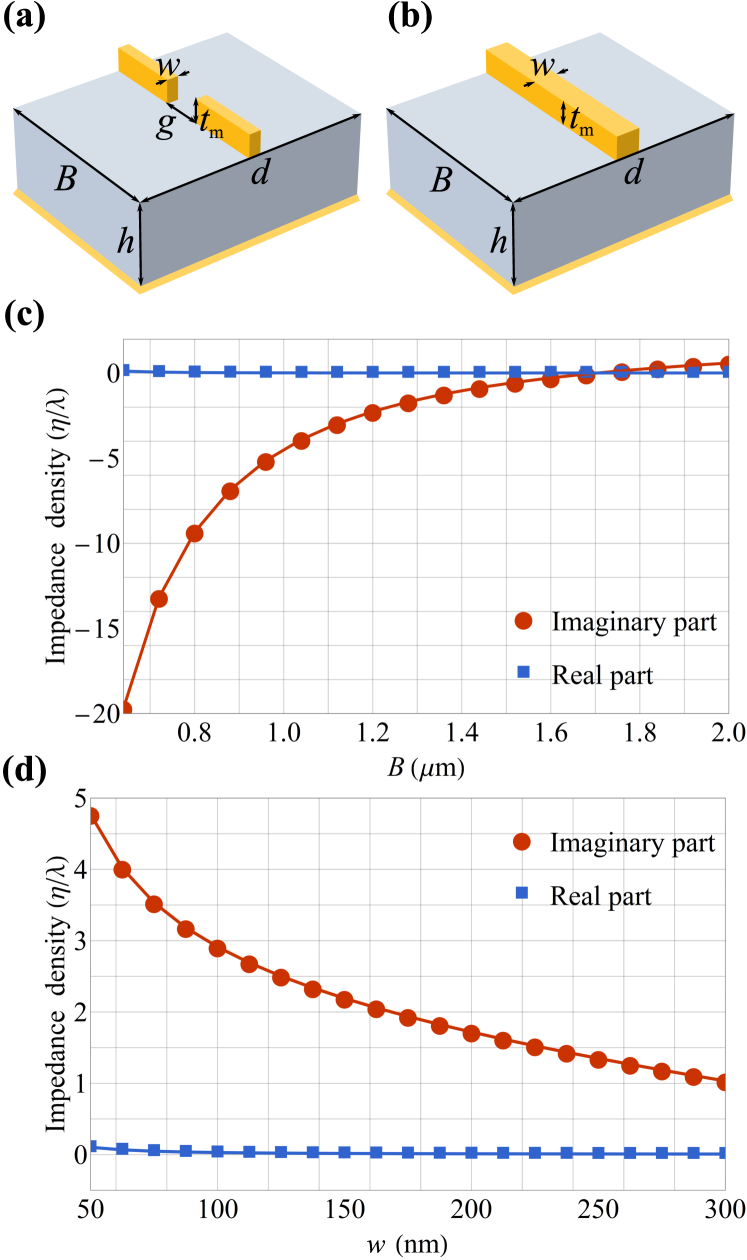
In this subsection we give an example of possible designs of unit cells that can be used as building blocks for metagratings operating at infrared frequencies. In what follows, the operation frequency is set to THz corresponding to the vacuum wavelength of m. In order to implement capacitive and inductive unit cells for infrared domain we consider metallic (gold) patches and wires. Gold elements are placed on a dielectric substrate (silicon dioxide) backed with gold as illustrated in Figs. 5 (a) and (b). The capacitive response is attributed to the gap between two patches. By changing the size of the gap or the size of patches one is able to adjust the capacitance. The inductance of a metallic wire is determined only by the cross section area. Although the design of the unit cells is relatively simple, it allows one to obtain impedance densities in a quite wide range of values as shown in Figs. 5 (c) and (d). Interestingly, the real part of the impedance density remains very small due to nonresonant response of the unit cells even though we take into account absorption in gold and silicon dioxide.
It is worthwhile to note that a single straight metallic wire may not be enough in case strong inductive response is necessary (large positive imaginary part of the impedance density). Cross section area is usually restricted by fabrication tolerances that does not allow one to infinitely reduce it. Meandering can be a solution (see Figs. 2 (c) and (e)) though it might complicate the fabrication.
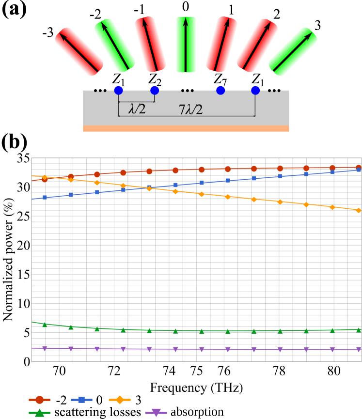
To validate calculated impedance densities we demonstrate a metagrating equally splitting a normally incident plane-wave between three propagating diffraction orders (-2, 0 and +3). The rest four propagating orders are cancelled, as presented by the schematic in Fig. 6 (a). Simulated frequency response of the metagrating is demonstrated in Fig. 6 (b). The incident wave equally (with an accuracy of a few percentages) excites chosen diffraction orders. One can see that the scattering in the -3, -1, +1 and +2 orders remains suppressed in a wide frequency range due to the nonresonant nature of the unit cells and that absorption constitutes only of total power. The level of scattering losses is rather a drawback of the approach presented in Ref. Popov et al. (2018), but can still be reduced as proposed by the design methodology of Ref. Popov et al. (2019).
To conclude this subsection, let us make a few practical comments. In the numerical simulations, dielectric permittivities of gold and silicon dioxide were taken from Refs. Babar and Weaver (2015) and Kischkat et al. (2012), respectively. Silicon dioxide was chosen as a substrate due to low losses and low refractive index at m. It allows one using a thick substrate while avoiding excitation of waveguide modes. On the other hand, if the dielectric substrate is thin, it may not be possible to model “wires” as having infinitely small cross section area and accurately account for the interaction with the substrate. Another practical feature is that between gold parts and a silicon dioxide substrate there is usually a thin chromium (or titanium) adhesion layer of a few nm thickness. Although all practical aspects should be taken into account while designing an experimental sample, we do not expect that the influence of such a thin intermediate layer can lead to a qualitative change and, therefore, did not consider it.
IV discussion and conclusion
In this work we have presented a simulation-based design approach to construct metagratings in the “unit cell by unit cell” manner. It represents an analog of the local periodic approximation that has been used to design space modulated metasurfaces and in comparison to a brute force numerical optimization (that deals straight with a whole supercell of a metagrating) can considerably reduce the time spent on the design. Indeed, assume that each unit cell constituting a -cells period of a metagrating has only one parameter to be adjusted and this parameter takes in total different values during a parametric sweep. Then, one would have to perform full-wave simulations in order to cover all possible combinations of parameters of unit cells and find optimal configuration of a metagrating’s supercell [assuming no “smart” algorithms (like genetic) are harnessed]. Clearly, this number strongly depends on the number of unit cells in a supercell . Meanwhile, the LPA deals with one unit cell at a time what makes the number of required full-wave simulations can be as small as and it does not depend on the number . We have validated the developed approach via 3D full-wave numerical simulations by demonstrating designs of metagratings controlling scattering patterns at microwave and infrared frequencies for both TE and TM polarizations. The both electric metagratings (TE polarization) required two different types of unit cells (capacitive and inductive) and overall we have performed only simulations, while the magnetic metagrating required one type of a unit cell and, thus, only simulations. Finally, simple and accurate analytical model describing metagratings allows one to take into account the impact of the metal-backed dielectric substrate and the interaction between “wires” composing the metagratings. It makes the local periodic approximation not only fast but also a rigorous approach to design metagratings represented by nonuniform arrays of “wires” (in bright contrast to metasurfaces).
In this work, we have considered a reflecting configuration of a 1D metagrating but the developed design approach can be generalized to deal also with transmitting and 2D metagratings. Up to date there are two methods to control transmission with metagratings: either by means of an asymmetric three-layer array Epstein and Rabinovich (2018) of electric-only “wires” or a single-layer array of bianisotropic particles Fan et al. (2018). In order to deal with 2D metagratings one would have to consider a 2D periodic array of point scatterers instead of a 1D array of line currents. In light of recently demonstrated acoustic metagratings Packo et al. (2019); Torrent (2018) we also expect that the LPA can be adjusted to design acoustic wavefront manipulation devices.
To conclude, wavefront control by means of metagratings is not only an innovative and efficient way to realize the transformation between incident and reflected and/or transmitted waves, but it also allows one to further reduce the fabrication complexity while significantly improving the performance and functionality of metagratings-based integrated optics components and reconfigurable antennas in microwave communication systems. In this respect, the developed approach can be an essential tool when designing complex passive or active metagratings across all electromagnetic spectrum.
acknowledgement
M.Y., J-L.P. and F.P. acknowledge financial support from ANR (grant mEtaNiZo).
Appendix A Retrieval of electric current and impedance density from specular reflection
In this section, we derive Eqs. (1) and (2). To that end we use analytical formulas for the electric field scattered by a -cells metagrating given in Ref. Popov et al. (2018). The system is excited by an incident plane wave with the electric field being along the -direction. Since in the LPA we simulate only a single “wire” per period, the electric field of the wave reflected from the periodic array depicted in Fig. 1 (b) can be represented via plane-wave expansion as follows
| (5) |
where and are, respectively, tangential and normal components of the wave vector of the diffraction order. The Fresnel’s reflection coefficient from the substrate backed by perfect electric conductor (PEC) is given by the following formula
| (6) |
where and . When a metal backing the dielectric substrate cannot be modeled as PEC, one has to correspondingly modify the reflection coefficient. The period and incidence angle are such that the only propagating diffraction order corresponds to the specular reflection (). Then, the amplitude of the zeroth diffraction order can be found from Eq. (A) to be
| (7) |
This formula is then used to express the current leading to Eq. (1).
In order to calculate the impedance density of a “wire” one needs to find the ratio between the total electric field at the position of a “wire” and the current in the “wire” (and then subtract the radiation resistance). can be represented by the sum of the external electric field , the electric field created by all other line currents and the field resulted from the reflection from the metal-backed substrate. The last two can be united and expressed as with the mutual-impedance density given by the following formula
| (8) |
Thus one arrives at the Eq. (2).
Appendix B Magnetic metagratings
A reflecting metagrating possessing magnetic-only response is modeled as a periodic array of magnetic line currents placed on top of a metal-backed dielectric substrate. In the first two subsections we derive analytical formulas (following Ref. Popov et al. (2018)) for the field radiated by such a system and describe the way towards control of diffraction patterns with magnetic metagratings. In the last subsection we derive Eqs. (3) and (4).
B.1 Radiation of an array of magnetic line currents
A single magnetic line current radiates a TM-polarized wave with the magnetic field being along the -direction (see Ref. Felsen and Marcuvitz (1994))
| (9) |
where is the Hankel function of the second kind and zeroth order. Consequently, the magnetic field radiated by a periodic array of magnetic line currents per period (see Fig. 1 (a)) is given by the series of Hankel functions
| (10) | |||||
where , and take integer values from to and from to , respectively. Since the array is periodic the field given by Eq. (10) can be expressed via the series of plane-waves by means of the Poisson’s formula (see Ref. Popov et al. (2018)) as follows
| (11) |
where .
The effect of the metal-backed dielectric substrate on the field radiated by the array can be derived following Ref. Rabinovich and Epstein (2018). After some algebra, one would arrive at the following expressions for the magnetic field profile outside the substrate ()
| (12) |
Here is the Fresnel’s reflection coefficient of a plane-wave (having tangential component of wave vector equal to ) from the metal-backed dielectric substrate
| (13) |
B.2 Controlling diffraction patterns with magnetic metagratings
| Impedance density () | |||||||
|---|---|---|---|---|---|---|---|
| Microwaves: TE | |||||||
| Infrared: TE | |||||||
| Admittance density () | |||||||
| Microwaves: TM | |||||||
| Geometrical parameters (mm) | |||||||
| Microwaves: TE | (cap. uc) | (cap. uc) | (ind. uc) | (ind. uc) | (cap. uc) | (cap. uc) | (cap. uc) |
| Geometrical parameters (mm) | |||||||
| Microwaves: TM | |||||||
| Geometrical parameters (nm) | |||||||
| Infrared: TE | (ind. uc) |
When a magnetic metagrating is illuminated by a TM-polarized plane-wave incident at angle , the scattered magnetic field can be represented as a superposition of plane-waves . Amplitudes of the plane-waves are found analytically (see previous subsection) and can be expressed as follows
| (14) |
where is the Kronecker delta representing the reflection of the incident wave from the metal-backed substrate. As in case of TE polarization described in Ref. Popov et al. (2018), Eq. (14) demonstrates that magnetic line currents contribute to the scattered plane-waves via the parameter . Magnetic line currents can be used to control plane-waves scattered in the far-field (). Since in practice it is more straightforward to deal with passive structures and also the excitation of magnetic line currents can be of particular difficulty, we are interested in the case when magnetic line currents are polarization currents excited by the incident plane wave in thin “wires” characterized by admittance densities . Then, necessary currents can be obtained by choosing admittance densities from the following equation
| (15) |
The right-hand side of Eq. (15) represents the total magnetic field at the location of the “wire”, where is the external magnetic field, are the mutual-impedance densities which account for the interaction with the substrate and adjacent “wires”. The magnetic field created by line current from all periods (except the zeroth one) is given by the following series
| (16) |
The magnetic field created by all other line currents can be accounted for as follows
| (17) |
Eventually, the waves reflected from the metal-backed substrate create the following magnetic field at the location of the “wire” (zeroth period)
| (18) |
In contrast to the case of TE polarization discussed in Refs. Rabinovich and Epstein (2018); Popov et al. (2018), the series in Eq. (18) does not converge. Indeed, has as limit when goes to infinity and for large . Meanwhile, it is well known that the harmonic series is divergent. However, the divergence in Eq. (18) is artificial and was brought when using the Poisson’s formula (see Eq. (11)). Thus, we can avoid divergence by using the Poisson’s formula backwards. To that end, we perform the following transformation of the series in Eq. (18)
| (19) |
The first series on the right hand side of Eq. (19) is now converging while the second one contains the singularity and should be transformed by means of the Poisson’s formula in the following way
| (20) |
Summarizing Eqs. (16), (17), (18) and (B.2) one arrives at the explicit expression for the mutual-admittance density
| (21) |
It is worth to note that from the mathematical point of view, it is not strictly correct to represent a diverging series as a sum of two terms as it is done in Eq. (19). However, when comparing estimations of the mutual-admittance densities given by Eq. (B.2) with the ones obtained from 2D full-wave numerical simulations (see Ref. Popov et al. (2019)), we observed a good agreement between the two in case of low permittivity substrates (e.g., ). A more rigorous treatment is necessary for dealing analytically with high permittivity substrates.
B.3 Retrieval of magnetic current and admittance density from specular reflection
In this subsection, we derive Eqs. (3) and (4) of the main text following the same order as in Appendix A. The magnetic field of the wave reflected from the uniform array of magnetic line currents illustrated in Fig. 1 (b) can be represented via the plane-wave expansion as follows
| (22) |
The amplitude of specularly reflected plane-wave (the only propagating diffraction order, ) is then found to be (see also Eq. (14))
| (23) |
From this equation it is straightforward to arrive at Eq. (3).
Appendix C Parameters of metagratings shown in examples
Table 1 provides impedance (admittance) densities as well as geometrical parameters of the “wires” composing the metagratings demonstrated as examples in Section III.
References
- Kildishev et al. (2013) A. V. Kildishev, A. Boltasseva, and V. M. Shalaev, “Planar photonics with metasurfaces,” Science 339, 1232009 (2013).
- Glybovski et al. (2016) S. B. Glybovski, S. A. Tretyakov, P. A. Belov, Y. S. Kivshar, and C. R. Simovski, “Metasurfaces: From microwaves to visible,” Physics Reports 634, 1–72 (2016).
- Asadchy et al. (2018) V. S. Asadchy, A. Díaz-Rubio, and S. A. Tretyakov, “Bianisotropic metasurfaces: physics and applications,” Nanophotonics 7, 1069–1094 (2018).
- Yu and Capasso (2014) N. Yu and F. Capasso, “Flat optics with designer metasurfaces,” Nature materials 13, 139–150 (2014).
- Chen et al. (2016) H.-T. Chen, A. J. Taylor, and N. Yu, “A review of metasurfaces: physics and applications,” Reports on Progress in Physics 79, 076401 (2016).
- Capasso (2018) F. Capasso, “The future and promise of flat optics: a personal perspective,” Nanophotonics 7, 953–957 (2018).
- Yu et al. (2011) N. Yu, P. Genevet, M. A. Kats, F. Aieta, J.-P. Tetienne, F. Capasso, and Z. Gaburro, “Light propagation with phase discontinuities: Generalized laws of reflection and refraction,” Science 334, 333–337 (2011).
- Pfeiffer and Grbic (2013) C. Pfeiffer and A. Grbic, “Metamaterial Huygens’ surfaces: Tailoring wave fronts with reflectionless sheets,” Physical Review Letters 110, 1–5 (2013).
- Pozar et al. (1997) D. M. Pozar, S. D. Targonski, and H. D. Syrigos, “Design of millimeter wave microstrip reflectarrays,” IEEE Transactions on Antennas and Propagation 45, 287–296 (1997).
- Epstein and Eleftheriades (2016) A. Epstein and G. V. Eleftheriades, “Huygens’ metasurfaces via the equivalence principle: design and applications,” Journal of the Optical Society of America B 33, A31–A50 (2016).
- Luukkonen et al. (2008) O. Luukkonen, C. Simovski, G. Granet, G. Goussetis, D. Lioubtchenko, A. V. Raisanen, and S. A. Tretyakov, “Simple and accurate analytical model of planar grids and high-impedance surfaces comprising metal strips or patches,” IEEE Transactions on Antennas and Propagation 56, 1624–1632 (2008).
- Wang et al. (2018) X. C. Wang, A. Díaz-Rubio, A. Sneck, A. Alastalo, T. Mäkelä, J. Ala-Laurinaho, J. F. Zheng, A. V. Räisänen, and S. A. Tretyakov, “Systematic design of printable metasurfaces: Validation through reverse-offset printed millimeter-wave absorbers,” IEEE Transactions on Antennas and Propagation 66, 1340–1351 (2018).
- Sell et al. (2017) David Sell, Jianji Yang, Sage Doshay, Rui Yang, and Jonathan A. Fan, “Large-angle, multifunctional metagratings based on freeform multimode geometries,” Nano Letters 17, 3752–3757 (2017), pMID: 28459583, https://doi.org/10.1021/acs.nanolett.7b01082 .
- Ra’di et al. (2017) Y. Ra’di, D. L. Sounas, and A. Alù, “Metagratings: Beyond the limits of graded metasurfaces for wave front control,” Phys. Rev. Lett. 119, 067404 (2017).
- Epstein and Rabinovich (2017) A. Epstein and O. Rabinovich, “Unveiling the properties of metagratings via a detailed analytical model for synthesis and analysis,” Phys. Rev. Applied 8, 054037 (2017).
- Popov et al. (2018) V. Popov, F. Boust, and S. N. Burokur, “Controlling diffraction patterns with metagratings,” Phys. Rev. Applied 10, 011002 (2018).
- Chen et al. (2018) M. Chen, E. Abdo-Sánchez, A. Epstein, and G. V. Eleftheriades, “Theory, design, and experimental verification of a reflectionless bianisotropic huygens’ metasurface for wide-angle refraction,” Phys. Rev. B 97, 125433 (2018).
- Popov et al. (2019) V. Popov, F. Boust, and S. N. Burokur, “Constructing the near field and far field with reactive metagratings: Study on the degrees of freedom,” Phys. Rev. Applied 11, 024074 (2019).
- Chalabi et al. (2017) H. Chalabi, Y. Ra’di, D. L. Sounas, and A. Alù, “Efficient anomalous reflection through near-field interactions in metasurfaces,” Phys. Rev. B 96, 075432 (2017).
- Rabinovich and Epstein (2018) O. Rabinovich and A. Epstein, “Analytical design of printed circuit board (pcb) metagratings for perfect anomalous reflection,” IEEE Transactions on Antennas and Propagation 66, 4086–4095 (2018).
- Tretyakov (2003) S. Tretyakov, Analytical modeling in applied electromagnetics (Artech House, Norwood, MA, 2003).
- Felsen and Marcuvitz (1994) L. B. Felsen and N. Marcuvitz, Radiation and scattering of waves, Vol. 31 (John Wiley & Sons, New York, 1994).
- Marqués et al. (2002) R. Marqués, F. Medina, and R. Rafii-El-Idrissi, “Role of bianisotropy in negative permeability and left-handed metamaterials,” Phys. Rev. B 65, 144440 (2002).
- Sauviac et al. (2004) B. Sauviac, C. R. Simovski, and S. A. Tretyakov, “Double split-ring resonators: Analytical modeling and numerical simulations,” Electromagnetics 24, 317–338 (2004), https://doi.org/10.1080/02726340490457890 .
- Babar and Weaver (2015) S. Babar and J. H. Weaver, “Optical constants of Cu, Ag, and Au revisited,” Appl. Opt. 54, 477–481 (2015).
- Kischkat et al. (2012) J. Kischkat, S. Peters, B. Gruska, M. Semtsiv, M. Chashnikova, M. Klinkmüller, O. Fedosenko, S. Machulik, A. Aleksandrova, G. Monastyrskyi, Y. Flores, and W. T. Masselink, “Mid-infrared optical properties of thin films of aluminum oxide, titanium dioxide, silicon dioxide, aluminum nitride, and silicon nitride,” Appl. Opt. 51, 6789–6798 (2012).
- Epstein and Rabinovich (2018) A. Epstein and O. Rabinovich, “Perfect anomalous refraction with metagratings,” IET Conference Proceedings , 479 (5 pp.) (2018).
- Fan et al. (2018) Z. Fan, M. R. Shcherbakov, M. Allen, J. Allen, B. Wenner, and G. Shvets, “Perfect diffraction with multiresonant bianisotropic metagratings,” ACS Photonics 5, 4303–4311 (2018).
- Packo et al. (2019) P. Packo, A. N. Norris, and D. Torrent, “Inverse grating problem: Efficient design of anomalous flexural wave reflectors and refractors,” Phys. Rev. Applied 11, 014023 (2019).
- Torrent (2018) D. Torrent, “Acoustic anomalous reflectors based on diffraction grating engineering,” Phys. Rev. B 98, 060101 (2018).