Computational RAM to Accelerate String Matching at Scale
Abstract
Traditional Von Neumann computing is falling apart in the era of exploding data volumes as the overhead of data transfer becomes forbidding. Instead, it is more energy-efficient to fuse compute capability with memory where the data reside. This is particularly critical for pattern matching, a key computational step in large-scale data analytics, which involves repetitive search over very large databases residing in memory. Emerging spintronic technologies show remarkable versatility for the tight integration of logic and memory. In this paper, we introduce CRAM-PM, a novel high-density, reconfigurable spintronic in-memory compute substrate for pattern matching.
1 Introduction
Classical computing platforms are not optimized for efficient data transfer, which complicates large-scale data analytics in the presence of exponentially growing data volumes. Imbalanced technology scaling further exacerbates this situation by rendering data communication, and not computation, a critical bottleneck [1]. Specialization in hardware cannot help in this case unless conducted in a data-centric manner.
Tight integration of compute capability into the memory, Processing in memory (PIM), is especially promising as the overhead of data transfer becomes forbidding at scale. The rich design space for PIM spans full-fledged processors and co-processors residing in memory [2]. Until the emergence of 3D-stacking, however, the incompatibility of the state-of-the-art logic and memory technologies prevented practical prototype designs. Still, 3D-stacking can only achieve processing near memory, PNM [3, 4, 5]. The main challenge remains to be fusing compute and memory without violating array regularity.
Emerging spintronic technologies show remarkable versatility for the tight integration of logic and memory. This paper introduces a high-density, reconfigurable spintronic in-memory compute substrate for pattern matching, CRAM-PM, which fuses compute and memory by adding an extra transistor to the standard magnetic tunnel junction (MTJ) based memory cell [6, 7]. Thereby each memory cell can participate in gate-level computation as an input or as an output. Computation is not disruptive, i.e., memory cells acting as gate inputs do not loose their stored values.
CRAM-PM can implement different types of basic Boolean gates to form a functionally complete set, therefore there is no fundamental limit to the types of computation that the array can perform. Each row can have only one active gate at a time, however, computation in all rows can proceed in parallel. CRAM-PM provides true in-memory computing by reconfiguring cells within the memory array to implement logic functions. As all cells in the array are identical, inputs and outputs to logic gates do not need to be confined to a specific physical location in the array. In other words, CRAM-PM can intiate computation at any location in the memory array.
Pattern matching is at the core of many important large-scale data analytics applications, ranging from bioinformatics to cryptography. The most prevalent form is string matching via repetitive search over very large reference databases residing in memory. Therefore, compute substrates such as CRAM-PM, that collocate logic and memory to prevent slow and energy-hungry data transfers at scale, have great potential.
In this case, each step of computation attempts to map a short character string to (the most similar substring of) an orders-of-magnitude-longer character string, and repeats this process for a very large number of short strings, where the longer string is fixed and acts as a reference.
In the following, we analyze a proof-of-concept CRAM-PM array for large-scale string matching. Specifically, Section 2 covers the basics of how CRAM-PM fuses compute with memory; Section 3 introduces a CRAM-PM implementation for pattern (string) matching; Sections 4, 5 provide the evaluation; Section 6 compares and contrasts CRAM-PM to related works; and Section 7 concludes the paper.
2 Background
2.1 Fusing Compute and Memory
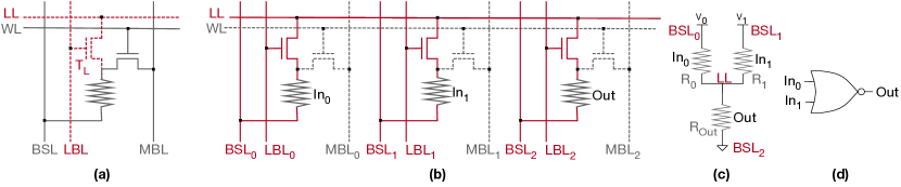
Without loss of generality, we adapt Computational RAM (CRAM) [8] as the spintronic PIM substrate to design CRAM-PM arrays in this study. In its most basic form, a CRAM array is essentially a 2D magneto-resistive RAM (MRAM). When compared to the standard 1T(ransistor)1M(TJ) MRAM cell, however, each CRAM cell features an additional transistor (Fig.1(a)), which acts as a switch between memory and logic configurations. A CRAM cell can operate as a regular MRAM memory cell or serve as an input/output to a logic gate.
Each MTJ consists of two layers of ferromagnets, termed as pinned and free layers, separated by a thin insulator. The magnetic spin orientation of the pinned layer is fixed; of the free layer, controllable. Changing the orientation of the free layer entails passing a (polarized) current through the MTJ, where the current direction sets the orientation. The relative orientation of the free layer with respect to the pinned layer, i.e., anti-parallel (AP) or parallel (P), gives rise to two distinct MTJ resistance levels, i.e., and , which encode logic 1 and 0, respectively. As resistance levels represent logic states, Fig.1 depicts each MTJ by its resistance.
Memory Configuration: The dashed components in Fig.1(a) capture all add-ons to the standard MRAM memory cell, in order to support logic functions. When the array is configured as memory, the Logic Bit Line (LBL) is set to 0 to turn the switch off, and thereby to disconnect the cells from the Logic Line (LL). In this case, the array becomes equivalent to a standard MRAM array. In the following, we detail the configuration for various memory operations (where LBL is always set to 0).
-
•
Data retention: The Word Line (WL) is set to 0 to isolate the cells and to prevent current flow through the MTJs.
-
•
Read: WL is set to 1, to connect each MTJ to its Bit Select Line (BSL) and Memory Bit Line (MBL). A small voltage pulse applied between BSL and MBL induces a current through the MTJ, which is a function of the resistance level (i.e., logic state), and which in turn a sense amplifier attached to BSL captures.
-
•
Write: WL is set to 1, to connect each MTJ to its BSL and MBL. A large enough voltage pulse (in the order of the supply voltage) is applied between BSL and MBL to induce a large enough current through the MTJ to change the spin orientation of the free layer.
Logic Configuration: LL connects all cells participating in computation, on a per row basis. Such cells may act as logic gate inputs or outputs. For each CRAM-PM cell participating in computation, WL is set to 0 to disconnect its MTJ from MBL. Instead, LBL is set to 1 to turn the switch on, which in turn connects the MTJ to the LL.
As an example, Fig.1(b) demonstrates the formation of a two input logic gate in the array, where cells labeled by “0”, “1”, and “2” correspond to the inputs , , and the output , respectively. Fig.1(c) depicts the equivalent circuit: BSL of the output, is grounded, while BSL of the two inputs, and are set to voltages and . The values of and determine the currents through the input MTJs, and , as a function of their resistance values and (i.e., logic states). flows through the output resistance . If is higher than the critical MTJ switching current , it will change the free layer orientation of ’s MTJ, and thereby, the logic state of . Otherwise, will keep its previous state.
We can easily expand this example to more than two inputs. The key observation is that we can change the logic state of the output as a function of the logic states of the inputs, within the array. And voltages at BSLs of the inputs dictate how such functions would look like.
| 0 () | 0 () | 1 | ||
| 0 () | 1 () | 0 | ||
| 1 () | 0 () | 0 | ||
| 1 () | 1 () | 0 |
Continuing with the example from Fig.1(b)/(c), let us try to implement an universal, 2-input NOR gate. Table 1 provides the truth table. would be 0 in this case for all input combinations but , , which incurs the lowest and , and hence, the highest . Let us refer to this value of as , following Table 1. Accordingly, if we pre-set to 0 (before computation starts), and determine and such that does exceed , while both and does not, would not switch from (its pre-set value) 0 to 1, for all input combinations but , .
As Boolean gates of practical importance (such as NOR) are commutative, a single voltage level at the BSLs of the inputs suffices to define a specific logic functionality. Each voltage level can serve as a signature for a specific logic gate. Accordingly, in the above example, applies, and its value simply follows from Kirchoff’s Laws, where , , and represent technology dependent constants. In the following, we will refer to this value as . In the example above, . While NOR gate is universal, we can implement different types of logic gates following a similar methodology for mapping the corresponding truth tables to the CRAM-PM array.
2.2 Basic Computational Blocks
We will next introduce basic CRAM-PM computational blocks for pattern matching, including inverters (INV), buffers (COPY), 3-input and 5-input majority (MAJ) gates, and 1-bit full adders.
INV: INV is a single-input gate. Still, we can follow a similar methodology to the NOR implementation (Table 1): Pre-set output to 0, and define in a way such that (), i.e., the current if the input is 0 (1), is higher (lower) than such that the output does (not) switch from the pre-set 0 to 1. By definition, applies, as .
COPY: For 1-bit copy, two back-to-back invocations of INV can suffice. A more time and energy efficient implementation, however, can perform the same function in one step as follows: Pre-set output to 1, and define in a way such that (), i.e., the current if the input is 0 (1), is higher (lower) than such that the output does (not) switch from the pre-set 1 to 0. By definition, applies, as .
MAJ: MAJ gates accept an odd number of inputs, and assign the majority (logic) state across all inputs to the output. The structure for a 3-input MAJ3 or 5-input MAJ5 gate is not any different from the circuit structure in Fig. 1(c) except the higher number of inputs. As an example, of the MAJ3 gate assumes its highest value for the 000 assignment of the three inputs – as the MTJ resistances of the three inputs, , , and , assume their lowest value for 000. Any input assignment having at least one 1, gives rise to a lower than ; and having at least two 1s, to an even lower . Finally, reaches its minimum for the input assignment 111, for which the input MTJs assume their highest resistance. Accordingly, we can pre-set the output to 1, and define in a way such that remains higher than if the three inputs have less than two 1s, such that switches from the pre-set 1 to 0, to match the input majority. We can symmetrically define , assuming a pre-set of 1.
XOR: XOR is an especially useful gate for comparison, however, a single-gate CRAM-PM implementation is not possible: In this case we need (not) to switch for 00 and 11, but not for 01 and 10, if the pre-set is 1 (0). However, due to , and assuming a pre-set of 1, we cannot let both and remain higher than (such that switches), while remain lower than (such that does not switch). The same observation holds for a pre-set of 0, as well.
| = | = | = | ||
| NOR(,) | COPY() | TH(,,,) | ||
| 0 | 0 | 1 | 1 | 0 |
| 0 | 1 | 0 | 0 | 1 |
| 1 | 0 | 0 | 0 | 1 |
| 1 | 1 | 0 | 0 | 0 |
We can implement XOR using a combination of universal CRAM-PM gates such as NOR. Thereby each XOR takes at least 4 steps (i.e., logic evaluations). For pattern matching, we will rely on a more efficient 3-step implementation (Table 2): In Step-1, we compute =NOR(,). In Step-2, we perform =COPY(). In the final Step-3, we invoke a 4-input thresholding TH function, which renders a 1 only if its inputs contain more than two zeros: = TH(,,,). TH has a pre-set of 0, and the operating principle is very similar to the majority gates except that TH accepts an even number of inputs. We can further optimize this implementation, and fuse Step-1 and Step-2 by implementing NOR as a two-output gate.

Full Adder:
A full adder has three inputs: , , and carry-in . The two
outputs are and the carry-out .
Like other logic functions, we can implement this adder using NOR gates.
However, an implementation based on a pair of MAJ gates
reduces the required number of steps significantly [9].
Fig.2 provides a step-by-step overview:
Step-1: = MAJ(,,)
Step-2: = INV()
Step-3: = COPY()
Step-4: = MAJ(,,,,)
2.3 Reconfigurability
Invoking a logic gate within the CRAM-PM array translates into pre-setting the output, connecting all cells participating in computation to LL by setting the corresponding LBLs (while keeping the WL at 0), grounding BSL of the output, and setting BSLs of the inputs to , which depends on the type of the logic gate. Therefore, modulo output pre-set, the complexity of reconfiguration is very similar to the complexity of addressing in the memory array. CRAM-PM is reconfigurable along two dimensions:
-
•
Each cell can serve as an input or as an output for a logic gate depending on the computational demands of the workload within the course of execution.
-
•
For a fixed input-output assignment, the logic function itself is reprogrammable. For example, we can reconfigure the gate from Fig.1(b)/(c) to implement another function than NOR by simply changing , to, e.g., (and applying a different output pre-set, as need be).
By default, CRAM-PM acts as an MRAM array. A dedicated architecturally visible set of registers keep the configuration bits to program CRAM-PM cells as logic gate input/outputs. These configuration bits capture not only the physical location in the array, but also whether the cell represents an input or an output, the pre-set value for the output, and . A fixed or floating portion of the CRAM-PM array can keep these configuration bits as part of the machine state, as well.
2.4 Row-level Parallelism
CRAM-PM can perform only one type of logic function in a row, at a time. This is because there is only one LL that spans the entire row, and any cell within the row to participate in computation gets directly connected to this LL (Section 2.1). On the other hand, the voltage levels on BSLs determine the type of the logic function, where each BSL spans an entire column. Furthermore, in each row, each LBL – which connects a cell participating in computation to LL – also spans an entire column. Therefore, all rows can perform the very same logic function in parallel, on the same set of columns.
In other words, CRAM-PM supports a special form of SIMD (single instruction multiple data) parallelism, where instruction translates into logic gate/operation; and data, into input cells in each row, across all rows, which span the very same columns.
To summarize, CRAM-PM can only have either all rows computing in parallel, or the entire array serving as memory. Regular memory reads and writes cannot proceed simultaneously with computation. Large scale pattern matching problems can greatly benefit from this execution model, as we are going to demonstrate in the following.
2.5 System Integration
CRAM-PM can serve as a stand-alone compute engine or a co-processor attached to a host processor. Following the near-memory processing taxonomy from [2], due to the reconfigurability (Section 2.3), both CRAM-PM design points still fall into the “programmable” class. A classic system has to specify how to offload both computation and data to the co-processor, and how to get the results back from the co-processor. For a CRAM-PM co-processor, we do not need to communicate data values – instead, the CRAM-PM array requires (ranges of) data addresses to identify the data to process, and the specification for computation, i.e., which function to perform on the corresponding data. In Section 3.3 we will detail this interface.
2.6 Spatio-Temporal Scheduling
The goal of classic memory data layout optimizations is to perform as many computations as possible per unit data delivered from the memory to the processor, as the data communication between the processor and the memory represents the bottleneck. CRAM-PM, on the other hand, brings compute capability to the data to be processed. The goal becomes minimizing the direct physical distance between the cells participating in computation. Considering that an output cell can serve as an input cell in subsequent steps of computation, the physical location of the cells carrying the input data for subsequent steps can dynamically change as computation proceeds.
This optimization problem gives rise to two strongly correlated sub-problems: the layout of data to be processed in the memory array, and the spatio-temporal scheduling of computations within the array. In this regard, the optimization problem has many analogies to floor-planning and placement algorithms deployed in the computer aided design of digital systems, which aim to minimize the “distance” (in terms of wire length) between interconnected circuit blocks. In CRAM-PM context, “interconnected blocks” translate into interconnected cells (over LL) participating in computation (Section 2.1). We will look closer into this effect in Section 3.4.
CRAM-PM hence features a unique trade-off between data replication and parallelism: Due to the internal array structure, (unless replicated), the same cell can only participate in one computational step at a time, which may impair opportunities for parallel execution. Data replication can unlock more parallelism in such cases, at the expense of a larger memory footprint.
3 Spintronic Pattern Matching
Pattern matching is a key computational step in large-scale data analytics. The most common form by far is character string matching, which involves repetitive search over very large databases residing in memory. Therefore, compute substrates such as CRAM-PM, that collocate logic and memory to avoid the latency and energy overhead of expensive data transfers, have great potential. Moreover, comparison operations dominate the computation, which represent excellent acceleration targets for CRAM-PM. As a representative and important large-scale string matching problem, in the following, we will use DNA sequence alignment [10] as a running example, and expand CRAM-PM’s evaluation to other string matching benchmarks in Section 5.
At each step, DNA sequence alignment tries to map a short character string to (the most similar substring of) an orders-of-magnitude-longer character string, and repeats this process for a very large number of short strings, where the longer string is fixed and acts as a reference. For each string, the characters come from the alphabet A(denine), C(ytosine), G(uanine), and T(hymine).
The long string represents a complete genome; short strings, short DNA sequences (from the same species). The goal is to extract the region of the reference genome to which the short DNA sequences correspond to. In the following, we will refer to each short DNA sequence as a pattern, and the longer reference genome as reference.
Aligning each pattern to the most similar substring of the reference usually involves character by character comparisons to derive a similarity score, which captures the number of character matches between the pattern and the (aligned substring of the) reference. Improving the throughput performance in terms of number of patterns processed per second in an energy-efficient manner is especially challenging, considering that a representative reference (i.e., the human genome) can be around characters long, that at least 2 bits are necessary to encode each character, and that a typical pattern dataset can have hundreds of millions patterns to match [11], where CRAM-PM can help due to reduced data transfer overhead and row-parallel comparison/similarity score computations.
Besides pattern matching, DNA sequence alignment algorithms include pre- and post-processing steps, which typically span (input) data transformation for more efficient processing, search space compaction, or (output) data re-formatting. In the following, we will only focus on the pattern matching operations, the execution time share of which can easily reach 88% in highly optimized GPU implementations of popular alignment algorithms [12] 111 For this implementation of the common BWA algorithm, the time share of the pattern matching kernel, inexact_match_caller, increases from 46% to 88%, as the number of base mismatches allowed (an input parameter to the algorithm) is varied from one to four (both representing typical values). .
Mapping any computational task to the CRAM-PM array translates into co-optimizing the data layout, data representation, and the spatio-temporal schedule of logic operations, to make the best use of CRAM-PM’s row-level parallelism (Section 2.4). This entails distribution of the data to be processed, i.e., the reference and the patterns, in a way such that each row can perform independent computations.
The data representation itself, i.e., how we encode each character of the pattern and the reference strings, has a big impact on both the storage and the computational complexity. Specifically, data representation dictates not only the type, but also the spatio-temporal schedule of (bit-wise) logic operations.
Spatio-temporal scheduling should also take intermediate results during computation into account, which may or may not be discarded (i.e., overwritten), and which may or may not overwrite existing data, as a function of the algorithm or array size limitations.
3.1 Data Layout & Data Representation
Without loss of generality, we use the data layout captured by Fig. 3, by folding the long reference over multiple CRAM-PM rows. Each row has four dedicated compartments to accommodate a fragment of the folded reference; one pattern; the similarity score (for the pattern when aligned to the corresponding fragment of the reference); and intermediate data (which we will refer to as scratch). The same format applies to each row, for efficient row-parallel processing. Each row contains a different fragment of the reference.

We determine the number of columns allocated for each of the four compartments, as follows: In the DNA alignment problem, the reference corresponds to a genome, therefore, can be very long. The species determine the length. As a case study for large-scale pattern matching, in this paper we will use approx. 3 character-long human genomes. Each pattern, on the other hand, represents the output from a DNA sequencing platform, which biochemically extracts the location of the four characters (i.e., bases) in a given (short) DNA strand. Hence, the sequencing technology determines the maximum length per pattern, and around 100 characters is typical for modern platforms processing short DNA strands [13]. The size of the similarity score compartment, to keep the character-by-character comparison results, is a function of the pattern length. Finally, the size of the scratch compartment depends on both the reference fragment and pattern length.
While the reference length and the pattern length are problem specific constants, the (reference) fragment length (as determined by the folding factor), is a CRAM-PM design parameter. By construction, each fragment should be at least as long as each pattern. The maximum fragment length, on the other hand, is limited by the maximum possible CRAM-PM row length, considering the maximum affordable capacitive load (hence, RC delay) on row-wide control lines such as WL and LL. However, row-level parallelism favors shorter fragments (for the same reference length). The shorter the fragments, the more rows would the reference occupy, and the more rows, hence regions of the reference, would be “pattern-matched” simultaneously.
For data representation, we simply use 2-bits to encode the four (base) characters, hence, each character-level comparison entails two bit-level comparisons.
3.2 Proof-Of-Concept CRAM-PM Design
CRAM-PM comprises two computational phases, which Algorithm 1 captures at the row-level: match, i.e., aligned bit-wise comparison and similarity score computation. As each row performs the very same computation in parallel, in the following, we will detail row-level operations.
In Algorithm 1, () and () represent the (character) length of the reference fragment and the pattern, respectively; and , the index of the fragment string where we align the pattern for comparison. The computation in each row starts with aligning the fragment and the pattern string, from the first character location of the fragment onward. For each alignment, a bit-wise comparison of the fragment and pattern characters comes next. The outcome is a () bits long string, where a 1 (0) indicates a character-wise (mis)match. We will refer to this string as the match string. Hence, the number of 1s in the match string acts as a measure for how similar the fragment and the pattern are, when aligned at that particular character location ( per Algorithm 1).
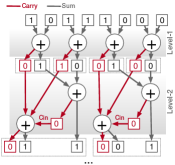
A reduction tree of 1-bit adders counts the number of 1s in the match string to derive the similarity score. Once the similarity score is ready, next iteration starts. This process continues until the last character of the pattern reaches the last character of the fragment, when aligned.
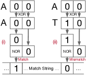
Phase-1 (Match, i.e., Aligned Comparison): Each aligned character-wise comparison gives rise to two bit-wise comparisons, each performed by an 2-input XOR gate. Fig.4a provides an example, where we compare the base character ‘A’ (encoded by ‘00’) of the fragment with the base character ‘A’ (i), and ‘T’ (encoded by ‘10’) (ii), of the pattern. A 2-input NOR gate converts the 2-bit comparison outcome to a single bit, which renders a 1 (0) for a character-wise (mis)match. Recall that a NOR gate outputs a 1 only if both of its inputs are 0, and that an XOR gate generates a 0 only if both of its inputs are equal. The implementation of these gates follows from Section 2.2.
CRAM-PM can only have one gate active per row at a time (Section 2.4). Therefore, for each alignment (i.e., for each or iteration of Algorithm 1), such a 2-bit comparison takes place () times in each row, one after another. Thereby we compare all characters of the aligned pattern to all characters of the fragment, before moving to the next alignment (at the next location per Algorithm 1). That said, each such 2-bit comparison takes place in parallel over all rows, where the very same columns participate in computation.
Phase-2 (Similarity Score Computation): For each alignment (i.e., iteration of Algorithm 1), once all bits of the match string are ready – i.e., the character-wise comparison of the fragment and the aligned pattern string is complete for all characters, we count the number of 1s in the match string to calculate the similarity score. A reduction tree of 1-bit adders performs the counting, as captured by Fig.4b, with the carry and sum paths shown explicitly for the first two levels. The top row corresponds to the contents of the match string; and each , to a 1-bit adder from Section 2.2.
(), the pattern length in characters, is equal to the match string length in bits. Hence, the number of bits required to hold the final bit-count (i.e., the similarity score) is . A naive implementation for the addition of () number of bits requires () steps, with each step using an -bit adder, to generate an -bit partial sum towards the -bit end result. For a typical pattern length of around 100 [13], this translates into approx. 100 steps, with each step performing a bit addition. Instead, to reduce both the number of steps and the operand width per step, we adopt the reduction tree of 1-bit adders from Fig.4b. Each level adds bits in groups of two, using 1-bit adders. For a typical pattern length of around 100 [13], we thereby reduce the complexity to 188 1-bit additions in total.
Data Output: Each iteration of Algorithm 1 at the end of Phase-2 generates a new similarity score in each row. One approach is, in each row, keeping the similarity score for all iterations. This requires (() ) bits per row, as each score takes bits, and one pass of Algorithm 1 takes (()) iterations. An alternative approach, to trade storage complexity for execution time, is using a dedicated score buffer at the array periphery (similar to the row buffer in main memory) to have each new score (per row) read out at the end of Phase-2, before the next iteration starts. In this case, each row only has space for one similarity score (of bits). This introduces an idle time window before the next iteration can fire, since we can only read out one score (from each row) at a time. Still, considering the overhead of pre-setting output cells to prepare for the next iteration, we can mask the overhead of read-outs. This trade-off strongly depends on the values of the fragment and pattern lengths.
In either case, CRAM-PM annotates each score with the row number and column number (in the folded reference) where the respective pattern was aligned. The column number simply corresponds to from Algorithm 1. The host processor can use this information to extract the maximum-score alignment, or to rank alignments for further analysis.
Assignment of Patterns to Rows: In each CRAM-PM array we can process a given pattern dataset in different ways. We can assign a different pattern to each row, where a different fragment of the reference resides, or distribute the very same pattern across all rows. Either option works as long as we do not miss the comparison of a given pattern to all fragments of the reference. In the following, we will stick to the second option, without loss of generality. This option eases capturing alignments scattered across rows (i.e., where two consecutive rows partially carry the most similar region of the reference to the given pattern). A large reference can also occupy multiple arrays and give rise to scattered alignments at array boundaries, which row replication at array boundaries can address.
3.3 System Interface
We will next cover the CRAM-PM system stack to support in-memory execution semantics for pattern matching.
CRAM-PM Instructions: In addition to conventional memory read and write, CRAM-PM instructions cover computational building blocks for in-memory pattern matching. CRAM-PM instructions hence form two classes: data transfer (read, write) and computational (arithmetic/logic). By construction, computational CRAM-PM instructions are block instructions: two dimensional vector instructions, which operate on all rows and on a subset of columns of an CRAM-PM array at a time. Hence, key operands for any computational CRAM-PM instruction are the column numbers of the source(s) (i.e., input(s) to computation) and destination(s) (i.e., output(s) to computation). Depending on the size of the pattern matching problem, multiple CRAM-PM arrays may be deployed in parallel. Therefore, the computational subset of CRAM-PM instructions facilitates gang-execution on all CRAM-PM arrays, as well. In the following, we will generically use the term CRAM-PM substrate to refer to all arrays participating in computation. We also make the distinction between macro- and micro-instructions. The set of micro-instructions covers actual bit-level operations performed in the CRAM-PM substrate, while the set of macro-instructions forms the high-level programming interface.
Programming Interface: To match CRAM-PM’s row-level parallelism, memory allocation and declaration of variables (which represent inputs and outputs to computation) happen at row granularity. Depending on the problem, a variable may cover the entire row or only a portion. The following code snippet provides an example, where an integer variable x gets written (assigned) to row r and column c in a CRAM-PM array (line 5):
1
2
3
4();
5(());
6();
In this case, besides x and y, ncell, val, c and r represent (already defined) integer values. The CRAM-PM-specific (composite) data type captures row and column coordinates for each variable stored in the array. in line 5 keeps this information for variable x, after it gets written to row r, from column c onwards, by the function. The subsequent read in line 6, conducted by the , directly assigns the value of x to y. CRAM-PM also features a read function, , which has a similar interface to with explicit row and column specification. We consider each such function as a macro-instruction.
The preset function in line 4 presets ncell number of (consecutive) cells, starting from column c, each to value val. CRAM-PM features different variants of this function, including one to gang-preset the entire scratch area (Fig. 3), and another where val is interpreted as a bitmask (of ncell bits) rather than a single-bit preset value which applies over the entire range of the specification.
Each pattern matching problem to be mapped to CRAM-PM features three basic stages:
-
(i)
Allocating and initializing the reference, pattern, and scratch regions in each array (Fig. 3);
-
(ii)
Computation;
-
(iii)
Collecting the pattern matching outcome.
Variants of preset and functions cover stage (i); and variants of , stage (iii). Stage (ii) can take different forms depending on the encoding of pattern and reference characters, but generally primitives such as () apply, which sums all cell contents between columns start and end, on a per row basis, and writes the result back where result points. macro-instruction can directly implement Phase-2 from Algorithm1 to calculate the bit-count on the match string (Section 3.2).
Code Generation: Code generation simply entails translating a sequence of macro-instructions to a sequence of micro-instructions for the CRAM-PM memory controller (SMC) to drive the in-place computation. Micro-instructions specify the type of operation and the columns to connect as inputs and outputs. For example, () specifies column as the output and column and as inputs to form a NAND gate in the CRAM-PM array. The macro-instruction , on the other hand, performs the very same operation on multi-bit operands (of width ncell): (). In this case, , , and still demarcate the starting columns for the source and destination (ncell bit) operands. hence translates into a sequence of ncell number of nand micro-instructions. For type of macro-instructions, on the other hand, a spatio-temporal scheduling pass (Section 2.6) determines the corresponding composition of micro-instructions. The goal is to maximize the throughput performance for the given data layout. This usually translates into masking the overhead of presets or other types of writes (per row) by coalescing when possible. By construction, variants of preset macro-instruction trigger a sequence of memory writes (as many as the number of rows), as at most one row can be written at a time.
CRAM-PM Memory Controller (SMC): SMC orchestrates computation in the CRAM-PM substrate, and the communication with the host processor. CRAM-PM features an internal clock. During computation, SMC allocates each micro-instruction a specific number of cycles to finish depending on the operation and operand widths. This time window includes peripheral overheads and the scheduling overhead due to SMC, besides computation. After the allocated time elapses (and unless an exception is the case), SMC fetches the next set of micro-instructions. SMC features an instruction cache where micro-instructions reside until they are issued to the CRAM-PM substrate. Before issue, SMC decodes the micro-instructions using a look-up table to initiate preset, and subsequently, to set the appropriate voltage level on input BSL (as a function of the operation, as explained in Section 2.2), before activating the corresponding columns in the specified arrays for computation. The look-up table keeps the voltage level and the preset value for each bit-level operation from Section 2.2, which form a CRAM-PM micro-instruction. No look-up table access is necessary for read and write operations.
3.4 Practical Considerations
Array Size: The maximum row width (i.e., the max. number of columns) per CRAM-PM array depends on the gate voltage (Section 2.1), the interconnect material for LL (which connects the input and output cells together in forming a gate), as well as the technology node. We conduct the following experiment to determine the max. row width: We consider a two-input, one output CRAM-PM gate which has the input cells and the output cell located in adjacent columns. In each experiment, we shift the output cell further away from the input cells, by one cell at a time. The process continues until we reach the terminating condition, which is when the current through the output cell falls below the required critical switching current for the most conservative input cell resistance states. Assuming copper interconnect segments of 160nm for LL, for representative CRAM-PM gates used in pattern matching, this analysis renders approximately 2K cells per row at 22nm, where the latency overhead induced by this max. distance computation barely reaches 1.7% of the switching time of the MTJ (assuming a near-term technology, as detailed in Section 4).
Array Periphery: Peripheral overheads, mainly induced by addressing and control operations, can play a vital role in determining the pattern matching throughput. Accordingly, throughout the evaluation, we consider the time and energy overhead of peripheral circuitry including row decoders, multiplexers, and sense amplifiers. For memory read and write operations a CRAM-PM array is not any different than a standard STT-MRAM array, hence we model periphery after the standard STT-MRAM. During computation, however, as all rows operate in parallel, row decoder overhead does not apply (which we conservatively keep). The periphery during computation rather becomes similar to the periphery of Pinatubo [14], an alternative spintronic PIM substrate (although CRAM-PM computation relies on a different mechanism, totally excluding sense amplifier involvement during computation contrary to Pinatubo). Even during computation where all rows are active, the current draw in an CRAM-PM array remains relatively modest. For example, using projections for long-term MTJ devices (as detailed in Section 4), a 128MB array would still consume considerably less current than a DDR3 SDRAM write operation [15].
Preset Overhead: Each logic operation requires the output to be (pre)set to a predefined value. Computation is row parallel, i.e., in all rows, the output cell resides in the very same column. Accordingly, before firing row-parallel computation, the corresponding column where the output cells reside should be preset. To this end, we can use a “gang” preset, which presets all cells in the output column simultaneously. The alternative is relying on the standard write operation, which can preset (columns in) one row at a time. Gang preset by definition is much faster than standard write based preset. The gang preset is equivalent to a parallel COPY operation – where all rows compute in parallel and where the output cells are all in the respective column subject to gang preset. Hence, the discussion about the periphery overhead during row-parallel computation directly applies here, and the current draw remains to be modest. For standard write based preset, on the other, the current draw is much less: As one gate can be actively computing in a row at a time, only one cell needs to be preset per row, and all rows are preset one after another.
4 Evaluation Setup
Technology Parameters: Table 3 provides technology parameters for a representative near-term and projected long-term MTJ based implementation. The critical current refers to an MTJ switching probability of 50%, which would incur a high write error rate (WER). To compensate, when deriving gate latency and energy values, we conservatively assume a 2 (5) larger for the near (long) term MTJ technology. We model access transistors after 22nm (HP) PTM [16].
| Near-term | Long-term | |
| MTJ Type | Interfacial PMTJ | Interfacial PMTJ |
| MTJ Diameter (nm) | 45 | 10 |
| TMR (%) | 133 [17] | 500 |
| RA Product () | 5 | 1 [18] |
| Critical Current () | 100 | 3.95 |
| Switching Latency () | 3 [19] | 1 [17] |
| () | 3.15 | 12.7 |
| () | 7.34 | 76.39 |
| Write Latency (ns) | 3.65 | 1.72 |
| Read Latency (ns) | 1.21 | 1.24 |
| Write Energy (pJ) | 0.36 | 0.308 |
| Read Energy (pJ) | 0.83 | 0.78 |
| (V) | 0.84–1.3 | 0.23–0.48 |
| (V) | 0.84–1.3 | 0.23–0.48 |
| (V) | 0.68–0.74 | 0.20–0.22 |
| (V) | 0.65–0.69 | 0.20–0.21 |
| (V) | 0.61–0.62 | 0.19–0.20 |
| (V) | 0.62–0.63 | 0.19–0.20 |
Simulation Infrastructure:
We developed a step-accurate simulator in C++ to capture the throughput
performance and energy consumption of CRAM-PM based pattern matching as a
function of the technology parameters.
We model the peripheral circuitry using NVSIM [20] to extract
the row decoder, mux, precharge, and sense amplifier induced energy and latency
overheads in CRAM-PM arrays used in the evaluation at 22nm.
Step-accurate simulation captures the overhead of each stage of pattern
matching:
(1) Write patterns on each row;
(2) Pre-set output cells (for comparison in match phase);
(3) Activate bitlines;
(4) Perform aligned comparison;
(5) Pre-set output cells (for similarity score computation phase);
(6) Activate bitlines;
(7) Compute score;
(8) Read-out score (optional).
Stages (2)-(4) are repeated for each bit of the pattern before moving to stage
(5), as an CRAM-PM row can only have one logic gate active at a time (i.e., we
can only perform one logic operation in a row at a time, but all rows can
compute that one operation simultaneously). Finally, stages (2)-(8) are repeated
for each alignment (each at a different location of the reference fragment,
per Algorithm 1), until the tails of the fragment and the pattern
meet.
Due to row-level parallelism, the execution time of all of these stages in an array
is equivalent to the execution time in any row.
We derive energy consumption from this execution model, as well, where
the energy consumption of an entire array corresponds to
the sum of the energy consumption of each individual row in the array.
Per array
energy multiplied by the total number of arrays required to hold the reference
gives us the total energy consumption.
Array Size & Organization: For each benchmark, we simply stick to a straight-forward 2-bit representation for each character, which yields the smallest possible array size. It is evident that, depending on the pattern matching problem at hand, we might need CRAM-PM arrays ranging from modest to very large in size. The thought provoking issue here is how to deal with sufficiently large arrays as it might restrict the design space, considering fabrication and circuit-level-design related limitations. As an example, the proof-of-concept implementation requires 300 arrays of 10K rows and around 2K columns each for the string matching case study from genomics. This renders a total size of roughly 24Mb per array, which is not excessively large. Still, the fabrication technology might not be mature enough to synthesize such an array. Commercial MRAM manufacturers address this challenge by banking. For example, EverSpin [21] uses 8 banks in its 256 Mb (Mb ) MRAM product. Distributing array capacity to banks helps satisfy the latency and energy requirement per access, as well. For CRAM-PM based pattern matching, we too are inclined to use a hierarchy of banks, to enhance scalability. While a clever data layout, operation scheduling and parallel activation of banks can mask the time overhead, the energy and area overhead would be largely due to replication of control hardware across banks. The most straight-forward option for banked CRAM-PM would be to treat each bank simply as an individual array which would map even shorter fragments of the reference to patterns from the input pattern dataset.
Benchmarks: We evaluate CRAM-PM using four pattern matching applications (which also include common computational kernels for pattern matching such as bit count), besides the running example of DNA sequence alignment throughout the paper. Table 4 tabulates these applications along with the corresponding problem sizes.
| Benchmark | Reference/Problem Size | Pattern Length | Array Size |
|---|---|---|---|
| DNA | 3G char. | 100 char. | 512512 |
| Bit count | 1000000 32-bit vectors | 1-bit | 512512 |
| String Matching | 10396542 words | 10 char. string | 512512 |
| Rivest Cipher 4 | 10396542 words | 248 bit | 10241024 |
| Word count | 1471016 words | 32 bits | 512512 |
DNA sequence alignment (DNA) is our running case study throughout the paper. We use a real human genome, NCBI36.54, from the 1000 genomes project [22] as the reference, and 4M 100-base character long real patterns from SRR1153470 [23].
Bit count (BC) [24] counts the number of ones in a set of vectors of fixed length. The counting consists of only addition of bits in the vectors and then adding all individual counts. The input vectors are mapped to the rows of CRAM-PM such that bit counting is performed in parallel.
String Match (SM) [25] matches a search string with a pre-stored reference string to identify the part of the reference string of the highest or lowest similarity. Space separated string segments and the search substring (which forms the pattern) itself are mapped to CRAM-PM rows such that all searches are performed in parallel.
Rivest Cipher 4 (RC4) is a popular stream cipher. Upon generating a cipher key, i.e., a string, it performs bitwise XOR on the cipher key and the text to cipher. The same key is used to decipher the text, as well. Segments of input text and the cipher key are mapped to CRAM-PM rows.
Word Count (WC) [25] counts the number of occurrence of specific words in an input text file, through word matching. The words are mapped to CRAM-PM rows along with search words, and the word matching in each row is executed concurrently.
Baselines for comparison: GPU Baseline: To quantify by how much a CRAM-PM based implementation of DNA sequence alignment provides improvement, we used a GPU implementation of the commonly used BWA algorithm [26]. We use the very same reference and input pattern pool for the GPU baseline and CRAM-PM mapped pattern matching application. Further, in order for the comparison to be fair, we only take the pattern matching portion of the GPU baseline into consideration (Section 3).
Near-Memory-Processing (NMP) Baseline: For throughput and energy characterization for near memory processing based pattern matching, we use an HMC model based on published data [3]. HMC power and latency models have contributions from three components: memory and logic layers, and communication links. To favor the NMP baseline, we ignore the power required to navigate the global wires between the memory controller and the logic layer, and intermediate routing elements. For logic layer, we consider single issue in-order cores, modeled after ARM Cortex A5 [27] with 1GHz clock and 32KB instruction and data caches. The cores have a peak power rating of 80mW, with dynamic power varying between 30mW and 60mW [28]. We first consider a total of 64 cores to provide parallel processing, which renders a total peak power of 5.12W. For communication, we assume an HMC-like configuration with four communication links operating at their peak frequency of 160 GB/s. To derive the throughput performance, we use the same reference and input patterns to profile each benchmark. We then use the instruction and memory traces to calculate the throughput. We validated this model through CasHMC [29] simulations. For reference, we also include a hypothetical NMP variant which includes 128 cores in the logic layer, and incurs zero memory overhead.
5 Evaluation
We will start the evaluation with detailed throughput performance and energy characterization, along with a sensitivity study, using DNA as a case study. Specifically, we will consider two design points, which differ in how the patterns (from the input pattern pool) get assigned to rows for matching. In other words, how patterns are scheduled for computation in the CRAM-PM array: The first one is a Naive implementation, where we take one pattern and blindly copy it to every row of all arrays to perform similarity search. The second implementation, on the other hand, features Oracular pattern scheduling, which can avoid assigning a pattern to a row where a too dissimilar (reference) fragment resides. Oracular is straight-forward to implement by adding a pre-processing step, where hash-based filtering is not uncommon [30]. We will leave exploration of this rich design space to future work. Any practical CRAM-PM implementation would fall somewhere in the spectrum between these two extremes.
Naive Design (): The caveat of this approach is that, since this design accepts one pattern at a time and aligns it naively to all reference fragments, the overhead of redundant computation is very large. Moreover, as a single pattern is matched to the entire reference, across all arrays, at a time, the apparent serialization hurts the throughput of the system, in terms of the number of patterns matched per second. In the following, we will refer to the number of patterns matched per second as match rate.
Oracular Pattern Scheduling (): The oracular scheduler resides between the input pattern pool and CRAM-PM, and controls to which row in which array each pattern goes. may still feed a given pattern to multiple rows, in multiple arrays, however, does not consider rows which carry a too dissimilar (reference) fragment. In other words, directs patterns to rows and arrays in a way such that achieving a high similarity score becomes more likely. While bases its pattern scheduling decisions on perfect information, a practical implementation of this idea would incur the overhead of gathering this information, i.e., extracting a schedule to keep pattern matching confined to rows where a high similarity score is more likely. In any case such smart scheduling of patterns benefits the throughput performance by reducing redundant computation which eats from the energy budget.
However, since all rows in a CRAM-PM array perform pattern matching (in lock-step but) in parallel, before computation begins, we require that all rows have their patterns ready. Scheduling patterns takes time, which might further affect the throughput performance of CRAM-PM, if we let the array sit idly, waiting for scheduling decisions to take place. We can mask this overhead, as drawing pattern scheduling decisions for all the rows in an array takes less time than writing patterns in the rows of that array. This, in effect, would not introduce any timing overhead towards the system throughput, although there is an energy overhead.
5.1 Throughput Performance and Energy Characterization
Fig.5 shows the throughput performance and energy efficiency, normalized to GPU baseline, for and , when processing a pool of 3M patterns. We use match rate (in terms of number of patterns processed per second) for throughput; match rate per milliwatt, for energy efficiency. yields very low throughput – by mapping each pattern to every row of each array at a time, and thereby increasing the total execution time significantly. pattern scheduling is very effective in eliminating this inefficiency: we observe that the throughput performance w.r.t. increases by approx. close to an order of magnitude in this case.
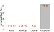
To put these throughput values in context, we can look at the time required to process the pool of 3M patterns, which is over 23215.3 hours, using 300 arrays under . The fundamental limitation for is the redundancy in computation. Since at a time, feeds only one pattern into all CRAM-PM arrays, the total time required to process the entire pool of patterns is higher. The effective throughput is limited by the time taken to align one pattern in one row. On the other hand, only takes about hours for the same pool of patterns. This drastic change in runtime is due to feeding multiple patterns into CRAM-PM arrays at the same time.
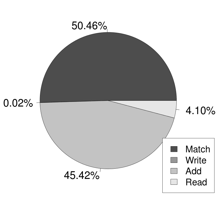

It is fundamental to the understanding of the performance and energy characterization to identify the individual contributions of actual computation stages – i.e., Stages(1)–(8) from Section 4. Fig.6 shows the distribution of energy and latency components. The preset overheads are 43.86% and 97.25% in energy and latency, respectively, where the bit-line (BL) driver energy and latency overheads are <1% and 2.7% respectively. The breakdowns in Fig.6 do not contain preset and BL driver related overheads. Apart from these, we observe that the majority of the energy (Fig.6a) is consumed by the match operations and additions during similarity score computations. However, in case of latency (Fig.6b), the dominant components change to read-outs of similarity scores (i..e, Stage (8)) and additions during similarity score computations. In case of both energy and latency, writes (i.e., Stage (1)) consume % of the share.
This breakdown clearly identifies preset overhead as the essential bottleneck. Also, although the time required by the match and similarity score compute phases are not drastically different, the energy required by the similarity score compute phase is around twice of that of match phase. Accordingly, we next look into preset and similarity score computation operations for optimization opportunities.
Optimized Designs (, ): As the reduction tree for addition (Fig.4b), which is at the core of similarity score computations, already represents an efficient design, we focus on optimizations to reduce the preset overhead. Since presets are inevitable for logic operations, it is not possible to entirely get rid of them. However, we can still hide preset latency through careful scheduling of presets.
As presets do not correspond to actual computation, and simply perform them in between computation. The challenge comes from successive steps in computation using the very same set of cells to implement logic functions. Instead of interrupting computation to preset these cells every time a few computation steps are completed, we can distribute such consecutive steps to different cells, using the scratch area from Fig.3, and preset them at once, before computation starts. We call the resulting designs and , respectively. The NaiveOpt and OracularOpt bars in Figure 5a and Figure 5b capture the resulting energy and throughput performance. We observe that, for each design option, energy consumption of the optimized case is unchanged. This is because the optimization only changes the scheduling of presets, where the total number of presets performed still remains the same. The throughput performance, on the other hand, skyrockets in both cases thanks to gang presets (Section 3.4).
Practical Considerations (Pattern Scheduling): The throughput we reported for is the theoretically achievable maximum. How close a practical implementation can come to this strongly depends on the actual values of the patterns, as well, which may or may not ease scheduling decisions. Since each array keeps consecutive fragments of the reference, it is always possible that patterns directed into a particular array do not have any matches in any of the rows. We may not always be able to eliminate such ill-schedules, depending on the pattern values, where the incurred redundant computation would degrade performance. The feasibility of any pattern scheduler is contingent upon the distribution of the patterns, in terms of the rows in the arrays where the most similar fragments reside.
5.2 Sensitivity Analysis
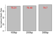
Sensitivity to Pattern Length: Up until now, we have used a pattern length of 100 characters. We will next examine the impact of pattern length on energy and throughput characteristics. Without loss of generality, we confine the analysis to . For the purpose of design space exploration, we experiment with pattern lengths of 200 and 300 characters, which are representative values for the alignment of short DNA sequences [13]. We keep the array structure the same, while the reference length remains fixed by construction. Fig.7 summarizes the outcome. Understandably, with the pattern length increasing, more computation becomes necessary to generate the similarity scores in each row. However, this effect does not directly translate into degraded performance: The throughput for increasing pattern lengths remains close to the baseline throughput for 100-character patterns. This is because the preset optimization is scalable. Increasing pattern length translates into more scratch bits for presets, which acts against throughput going down sharply. Irrespective of the application domain, the maximum pattern length is actually limited by technology constraints, since the required number of cells per row also increases with increasing pattern length. We further observe that the compute efficiency (i.e., the match rate per mW) decreases due to increases in computation per alignment, which is congruent with the intuition.

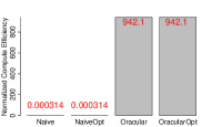
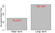
Sensitivity to MTJ Technology: MTJs have been able to meet technology trend estimations so far. We next consider the long-term technology projections from Table 3 for the default, representative pattern length of 100. Building upon OracularOpt, we will refer to this design as OracularOptProj. As Fig.8 indicates, a boost in match rate (i.e., throughput) and compute efficiency by approx. 2.15 becomes possible.
5.3 CRAM-PM vs. NMP
In the following we characterize benchmark applications, in terms of match rate and compute efficiency, when mapped in CRAM-PM vs. two baselines: NMP and a hypothetical variant of NMP with no memory overhead (NMP-Hyp).
Fig. 9 depicts the match rates of Oracular and OracularProj normalized to NMP and NMP-Hyp, respectively. Each bar is marked by the NMP baseline used for comparison. Overall, we observe that, both in near-term (Oracular) and long-term (OracularProj), CRAM-PM shows a significant improvement in throughput performance. The maximum improvement is 133552 (for WC) for long-term MTJ technology, due to good alignment of search and reference patterns in CRAM-PM. All applications have smaller improvement w.r.t. NMP-Hyp, both for near and long-term MTJ technologies, since NMP-Hyp has no memory overhead and hence has a much higher match rate than NMP to start with. Fig. 10 depicts the outcome for compute efficiency. Generally we observe a similar trend to match rate, with all benchmarks (but BC) featuring >5 improvement even w.r.t. the ideal baseline NMP-Hyp. Overall, BC shows the least benefit w.r.t. NMP-Hyp, since BC has a lower compute to memory access ratio and eliminating memory overhead greatly improves the NMP-Hyp throughput and compute efficiency. RC4 has the highest improvements of approx. 300 and 900, for near-term and long-term respectively, in compute efficiency due to CRAM-PM’s efficiency in handling its high number of XOR operations.
5.4 Gate-level Characterization
In this section, we compare the throughput performance of CRAM-PM with Ambit [31] and Pinatubo [14]. Ambit reports a comparative bulk throughput analysis with respect to CPU and GPU baselines, in executing basic logic operations on fixed sized vectors of one-bit operands. Pinatubo reports bit-wise throughput of OR operation only, on a bit long vector. We considered the highest throughput (for 128-row operation) reported by Pinatubo. To conduct a fair comparison, we assume the same vector size of 32MB used in Ambit. Fig.11 captures the outcome, w.r.t. Ambit, in terms of Giga operations per second (GOPs), for NOT, OR, NAND, and XOR implementations. We observe a higher throughput for CRAM-PM across all of these bitwise operations. Ambit achieves the highest throughput for NOT, where CRAM-PM performs approx. 178 and 370 better, considering near-term and projected long-term MTJ technologies (Section 4), respectively. The exploitation of row-level parallelism and lack of actual data transfer within the array – which is not the case for Ambit per Section6 – are the main reasons behind such improvement. The throughput of basic logic operations (i.e., NOT, OR, NAND) is very comparable to each other in CRAM-PM, unlike Ambit. For the more complex logic operation XOR, the throughput improvement for long-term, projected CRAM-PM is 4 over Ambit; whereas for near-term CRAM-PM, only 1.34. In comparison to OR throughput of Pinatubo, CRAM-PM is approx. and better for near-term and long-term, respectively. For this comparison, we do not optimize data layout or operation scheduling for CRAM-PM. That said, Ambit is based on a mature (DRAM) technology, and therefore more versatile for integration in conventional systems.
5.5 Impact of Process Variation
We conclude the evaluation with a discussion on the impact of process variation, which, due to imperfections in manufacturing technology, may result in significant deviation in device parameters from their expected values. Both access transistors and the MTJ in an CRAM-PM cell are subject to process variation. Since access transistors are fabricated using the relatively more mature CMOS technology, the effect of process variation is far less dominating than what was in it’s initial years. Being a relatively new technology, MTJ devices are more susceptible to process variation, which directly affects critical parameters such as switching current and switching latency. However, as MTJ technology matures, it is likely that it too will be able to reduce the impact of process variation.
One concern is variation in critical switching current, which can directly translate into variation in bias voltages on bitlines, i.e., , which determines the gate type. However, different CRAM-PM gates featuring close values (and hence may be subject to this type of variation) are usually distinguished either by a different value of the preset or a different number of inputs, which makes it unlikely that the gate functions would overlap with each other as a result of variation. We validated this observation assuming a variation in switching current by , and , respectively, for all evaluated gates implemented in the CRAM-PM array.
6 Related Work
Without loss of generality, we base CRAM-PM on the spintronic PIM substrate CRAM which was briefly presented in [8] and evaluated for a single-neuron digit recognizer along with a small scale 2D convolution in [32]. CRAM is unique in combining multi-grain (possibly dynamic) reconfigurability with true processing in memory semantics. The resistive Associative Processor [33] and DRAM-based DRAF [34] on the other hand, rely on look-up-tables to support reconfigurable fabrics like FPGA. The SRAM-based Compute Cache [35] can carry out different vector operations in the cache, but CRAM-PM needs a wider range of computations on much larger data than could fit in cache. Maintaining data coherence among cores which constitute near-memory logic is also an issue [36, 37] which is not the case for CRAM-PM due to the absence of dedicated cores (with full-fledged memory hierarchies) to implement logic operations.
CRAM-PM performs true in-memory computation using STT-MRAMs. The idea is configuring cells of the memory array as resistive dividers, since the state of an STT-MRAM cell corresponds to one of two resistance values. A comparable design based on memristors, MAGIC [38], also uses resistive division. Another work proposes an in-memory ReRAM based data parallel processor with SIMD ISA to implement complex functions for general purpose PIM [39]. Such arrays suffer from significant endurance issues when compared to STT-MRAMs. Recent proposals for bit-wise in memory computing include Ambit [31], Pinatubo [14] and STT-CiM [40]. Ambit [31] supports bitwise AND, OR, and NOT operations in DRAM, but only performs computation on a designated set of rows. Thus, to compute on an arbitrary row, the row must first be copied to these dedicated compute rows and then be copied back once the computation is complete. Pinatubo [14] on the other hand, can perform bitwise operations on data residing in multiple rows, using a specialized sense amplifier with variable reference voltage, which increases the susceptibility to variation. STT-CiM [40] is similar to Pinatubo, where multiple WL are activated to sense the logic function between data residing in participating rows. The difference is that STT-CiM supports more complex operations such as addition on top of basic Boolean functions. The threshold current to sense amplifier is changed to achieve different logic functionalities. STT-CiM is also more susceptible to variation due to the use of sense amplifiers to execute logic functions.
In [41], the functionality of human brain is imitated to solve pattern matching problems, where a learned hypervector is stored in a CAM structure and query patterns are matched one by one with the stored hypervector representation of reference pattern. While this approach might be suitable for approximate applications such as natural language processing, the inherent sequential nature of data processing limits the throughput. Also, the overhead of transforming data to a hypevector has a limiting contribution to the achievable throughput.
FELIX [42] proposes a crossbar of memristors, which forms logic gates following the same principle as CRAM. Although similar in concept, the majority and AND operations in FELIX are multi-cycle (vs. single cycle in CRAM-PM). Moreover, FELIX presents segmented bitlines (by inserting switches within bitlines) to make smaller arrays run in parallel and execute different operations on data. This approach can result in severe sneak current issues that can potentially prevent the design from functioning correctly.
7 Conclusion
This paper introduces CRAM-PM, a novel, reconfigurable spintronic compute substrate for true in-memory pattern matching, which represents a key computational step in large-scale data analytics. When configured as memory, CRAM-PM is not any different than an MRAM array. Each MRAM cell, however, can act as an input or output to a logic gate, on demand. Therefore, reconfigurability does not compromise memory density. Each row can have only one logic gate active at a time, but the very same logic operation can proceed in all rows (at the same columns) in parallel. We implement a proof-of-concept CRAM-PM array for large-scale character string matching to pinpoint design bottlenecks and aspects subject to optimization. The encouraging results from Section 5 indicate a great potential for throughput performance and energy efficiency.
References
- [1] M. Horowitz, “Computing’s Energy Problem (and What We Can Do About It),” Keynote at International Solid State Circuits Conference, February 2014.
- [2] G. H. Loh, N. Jayasena, M. Oskin, M. Nutter, and D. Roberts, “A Processing in Memory Taxonomy and a Case For Studying Fixed-function PIM,” in Workshop on Near-Data Processing in conjunction with MICRO, 2013.
- [3] “Hybrid Memory Cube (HMC).” http://www.hotchips.org/wp-content/uploads/hc_archives/hc23/HC23.18.3-m%emory-FPGA/HC23.18.320-HybridCube-Pawlowski-Micron.pdf.
- [4] “Hybrid Bandwidth Memory (HBM).” http://www.amd.com/en-us/innovations/software-technologies/hbm.
- [5] R. Nair, S. F. Antao, C. Bertolli, P. Bose, J. R. Brunheroto, T. Chen, C. Y. Cher, C. H. A. Costa, J. Doi, C. Evangelinos, B. M. Fleischer, T. W. Fox, D. S. Gallo, L. Grinberg, J. A. Gunnels, A. C. Jacob, P. Jacob, H. M. Jacobson, T. Karkhanis, C. Kim, J. H. Moreno, J. K. O’Brien, M. Ohmacht, Y. Park, D. A. Prener, B. S. Rosenburg, K. D. Ryu, O. Sallenave, M. J. Serrano, P. D. M. Siegl, K. Sugavanam, and Z. Sura, “Active Memory Cube: A Processing-in-Memory Architecture for Exascale Systems,” IBM Journal of R.&D., vol. 59, no. 2/3, 2015.
- [6] A. Lyle, J. Harms, S. Patil, X. Yao, D. J. Lilja, and J.-P. Wang, “Direct Communication between Magnetic Tunnel Junctions for Nonvolatile Logic Fanout Architecture,” Applied Physics Letters, vol. 97, no. 152504, 2010.
- [7] H. M. Jianguo Wang and J.-P. Wang, “Programmable Spintronics Logic Device Based on a Magnetic Tunnel Junction Element,” Applied Physics Letters, vol. 97, no. 10D509, 2005.
- [8] Z. Chowdhury, J. D. Harms, S. K. Khatamifard, M. Zabihi, Y. Lv, A. P. Lyle, S. S. Sapatnekar, U. R. Karpuzcu, and J.-P. Wang, “Efficient in-memory processing using spintronics,” IEEE Computer Architecture Letters, vol. 17, no. 1, pp. 42–46, 2018.
- [9] C. Augustine, G. Panagopoulos, B. Behin-Aein, S. Srinivasan, A. Sarkar, and K. Roy, “Low-power Functionality Enhanced Computation Architecture Using Spin-based Devices,” in International Symposium on Nanoscale Architectures, 2011.
- [10] Z. D. Stephens, S. Y. Lee, F. Faghri, R. H. Campbell, C. Zhai, M. J. Efron, R. Iyer, M. C. Schatz, S. Sinha, and G. E. Robinson, “Big Data: Astronomical or Genomical?,” PLOS Biology, vol. 13, July 2015.
- [11] S. S. Ajay, S. C. Parker, H. O. Abaan, K. V. F. Fajardo, and E. H. Margulies, “Accurate and comprehensive sequencing of personal genomes,” Genome Research, vol. 21, no. 9, 2011.
- [12] P. Klus, S. Lam, D. Lyberg, M. S. Cheung, G. Pullan, I. McFarlane, G. S. Yeo, and B. Y. Lam, “Barracuda-a fast short read sequence aligner using graphics processing units,” BMC research notes, vol. 5, no. 1, p. 27, 2012.
- [13] “Illumina sequencing by synthesis (SBS) technology: https://www.illumina.com/technology/next-generation-sequencing/sequenci%ng-technology.html.”
- [14] S. Li, C. Xu, Q. Zou, J. Zhao, Y. Lu, and Y. Xie, “Pinatubo: A processing-in-memory architecture for bulk bitwise operations in emerging non-volatile memories,” in Design Automation Conference (DAC), 2016 53nd ACM/EDAC/IEEE, pp. 1–6, IEEE, 2016.
- [15] “Micron tn-41-01: Calculating memory system power for ddr3.”
- [16] “Predictive technology Model.” http://ptm.asu.edu/.
- [17] G. Jan, L. Thomas, S. Le, Y. J. Lee, H. Liu, J. Zhu, R. Y. Tong, K. Pi, Y. J. Wang, D. Shen, R. He, J. Haq, J. Teng, V. Lam, K. Huang, T. Zhong, T. Torng, and P. K. Wang, “Demonstration of fully functional 8Mb perpendicular STT-MRAM chips with sub-5ns writing for non-volatile embedded memories,” in Symposium on VLSI Technology (VLSI-Technology), June 2014.
- [18] H. Maehara, K. Nishimura, Y. Nagamine, K. Tsunekawa, T. Seki, H. Kubota, A. Fukushima, K. Yakushiji, K. Ando, and S. Yuasa, “Tunnel Magnetoresistance above 170% and Resistance–Area Product of 1 Ohm(micro-m)2 Attained by In situ Annealing of Ultra-Thin MgO Tunnel Barrier,” Applied Physics Express, vol. 4, no. 3, 2011.
- [19] H. Noguchi, K. Ikegami, K. Kushida, K. Abe, S. Itai, S. Takaya, N. Shimomura, J. Ito, A. Kawasumi, H. Hara, and S. Fujita, “7.5 A 3.3ns-access-time 71.2 microW/MHz 1Mb embedded STT-MRAM using physically eliminated read-disturb scheme and normally-off memory architecture,” in IEEE International Solid-State Circuits Conference (ISSCC), Feb 2015.
- [20] X. Dong, C. Xu, N. Jouppi, and Y. Xie, “NVSim: A circuit-level performance, energy, and area model for emerging non-volatile memory,” in Emerging Memory Technologies, pp. 15–50, Springer, 2014.
- [21] “Everspin Technologies.” https://www.everspin.com/.
- [22] “1000 genomes project.” ftp://ftp-trace.ncbi.nih.gov/1000genomes/ftp/technical/reference/.
- [23] “SRR1153470.” https://trace.ncbi.nlm.nih.gov/Traces/sra/?run=SRR1153470.
- [24] M. R. Guthaus, J. S. Ringenberg, D. Ernst, T. M. Austin, T. Mudge, and R. B. Brown, “Mibench: A free, commercially representative embedded benchmark suite,” in Workload Characterization, 2001. WWC-4. 2001 IEEE International Workshop on, pp. 3–14, IEEE, 2001.
- [25] C. Ranger, R. Raghuraman, A. Penmetsa, G. Bradski, and C. Kozyrakis, “Evaluating mapreduce for multi-core and multiprocessor systems,” in High Performance Computer Architecture, 2007. HPCA 2007. IEEE 13th International Symposium on, pp. 13–24, Ieee, 2007.
- [26] R. Li, Y. Li, K. Kristiansen, and J. Wang, “Soap: short oligonucleotide alignment program,” Bioinformatics, vol. 24, no. 5, 2008.
- [27] “Cortex-A5 Processor.” http://www.arm.com/products/processors/cortex-a/cortex-a5.php/.
- [28] S. H. Pugsley, J. Jestes, H. Zhang, R. Balasubramonian, V. Srinivasan, A. Buyuktosunoglu, A. Davis, and F. Li, “NDC: Analyzing the impact of 3D-stacked memory+ logic devices on mapreduce workloads,” in Performance Analysis of Systems and Software (ISPASS), 2014 IEEE International Symposium on, pp. 190–200, IEEE, 2014.
- [29] D. Jeon and K. Chung, “Cashmc: A cycle-accurate simulator for hybrid memory cube,” IEEE Computer Architecture Letters, vol. 16, pp. 10–13, Jan 2017.
- [30] J. Kim, D. Senol, H. Xin, D. Lee, M. Alser, H. Hassan, O. Ergin, C. Alkan, and O. Mutlu, “Genome read in-memory (grim) filter: Fast location filtering in dna read mapping using emerging memory technologies https://people.inf.ethz.ch/omutlu/pub/GRIM-genome-read-in-memoryfilter_psb17-poster.pdf,” 2017.
- [31] V. Seshadri, D. Lee, T. Mullins, H. Hassan, A. Boroumand, J. Kim, M. A. Kozuch, O. Mutlu, P. B. Gibbons, and T. C. Mowry, “Ambit: In-memory accelerator for bulk bitwise operations using commodity DRAM technology,” in Proceedings of the 50th Annual IEEE/ACM International Symposium on Microarchitecture, MICRO-50 ’17, (New York, NY, USA), pp. 273–287, ACM, 2017.
- [32] M. Zabihi, Z. Chowdhury, Z. Zhao, U. R. Karpuzcu, J.-P. Wang, and S. Sapatnekar, “In-memory processing on the spintronic cram: From hardware design to application mapping,” IEEE Transactions on Computers, 2018.
- [33] L. Yavits, S. Kvatinsky, A. Morad, and R. Ginosar, “Resistive Associative Processor,” CAL, vol. 14, no. 2, 2015.
- [34] M. Gao, C. Delimitrou, D. Niu, K. T. Malladi, H. Zheng, B. Brennan, and C. Kozyrakis, “DRAF: A Low-power DRAM-based Reconfigurable Acceleration Fabric,” ISCA, 2016.
- [35] S. Aga, S. Jeloka, A. Subramaniyan, S. Narayanasamy, D. Blaauw, and R. Das, “Compute Caches,” HPCA, 2017.
- [36] A. Boroumand, S. Ghose, M. Patel, H. Hassan, B. Lucia, K. Hsieh, K. T. Malladi, H. Zheng, and O. Mutlu, “LazyPIM: An Efficient Cache Coherence Mechanism for Processing-in-Memory,” CAL, vol. 16, Jan 2017.
- [37] M. Gao, G. Ayers, and C. Kozyrakis, “Practical Near-Data Processing for In-Memory Analytics Frameworks,” in PACT, 2015.
- [38] S. Kvatinsky, D. Belousov, S. Liman, G. Satat, N. Wald, E. G. Friedman, A. Kolodny, and U. C. Weiser, “MAGIC: Memristor-aided logic,” IEEE Transactions on Circuits and Systems II: Express Briefs, vol. 61, Nov 2014.
- [39] D. Fujiki, S. Mahlke, and R. Das, “In-Memory Data Parallel Processor,” in Proceedings of the Twenty-Third International Conference on Architectural Support for Programming Languages and Operating Systems, pp. 1–14, ACM, 2018.
- [40] S. Jain, A. Ranjan, K. Roy, and A. Raghunathan, “Computing in memory with spin-transfer torque magnetic ram,” IEEE Transactions on Very Large Scale Integration (VLSI) Systems, vol. 26, pp. 470–483, March 2018.
- [41] M. Imani, A. Rahimi, D. Kong, T. Rosing, and J. M. Rabaey, “Exploring hyperdimensional associative memory,” in 2017 IEEE International Symposium on High Performance Computer Architecture (HPCA), pp. 445–456, Feb 2017.
- [42] S. Gupta, M. Imani, and T. Rosing, “Felix: fast and energy-efficient logic in memory,” in Proceedings of the International Conference on Computer-Aided Design, p. 55, ACM, 2018.