Strategy for accurate thermal biasing at the nanoscale
Abstract
We analyze the benefits and shortcomings of a thermal control in nanoscale electronic conductors by means of the contact heating scheme. Ideally, this straightforward approach allows one to apply a known thermal bias across nanostructures directly through metallic leads, avoiding conventional substrate intermediation. We show, by using the average noise thermometry and local noise sensing technique in InAs nanowire–based devices, that a nanoscale metallic constriction on a substrate acts like a diffusive conductor with negligible electron-phonon relaxation and non-ideal leads. The non-universal impact of the leads on the achieved thermal bias — which depends on their dimensions, shape and material composition — is hard to minimize, but is possible to accurately calibrate in a properly designed nano-device. Our results allow to reduce the issue of the thermal bias calibration to the knowledge of the heater resistance and pave the way for accurate thermoelectric or similar measurements at the nanoscale.
Introduction
Managing nanoscale electronic devices out of thermal equilibrium is an outstanding problem both from the fundamental [1, 2] and applied perspectives [3]. Unlike cooling the electrons down by refrigeration [4, 5], raising their temperature above the thermal bath is achieved easily by Joule heating of the whole device [6], of a part of it [7, 8, 9] or of the nearby substrate [10, 11, 12, 13, 14, 15, 16]. Accurate control of the generated thermal bias, which is an obvious prerequisite for a quantitative measurement in thermoelectric (TE) and other similar experiments [17, 18], remains a separate complex problem. This is especially true for the electronic transport at nanoscale, when the dimensions of the device under test are small compared to the inelastic length scales, whereas the available current leads are too small to be treated as ideal macroscopic reservoirs.
Various non-equilibrium control tools are capable of measuring the temperature of the electronic [4, 19, 7, 8] and lattice sub-systems [20], including spatially resolved [21, 9, 22, 23], time resolved [24, 25] and energy resolved [26, 27] approaches. However, the accuracy of the control is strongly outweighed by the tools’ complexity. Moreover, the modeling of the heat balance at nanoscale is often not reliable, for the a-priori unknown electron-phonon coupling [19], thermal contact resistance [10, 28, 29, 30, 31] and lattice thermal conductivity [32, 33, 29]. For instance, as demonstrated recently by some of us, below K the electron and lattice systems are practically decoupled in InAs nanowires (NWs) [8]. As a result, the substrate heating is inefficient for thermal biasing [34] manifesting a failure of such an approach in this temperature range. Not to mention that the thermal bias calibration by means of the metallic resistance thermometry [35] loses its sensitivity within the residual resistance range at low temperatures and is complicated for heaters shorter than the electron-phonon relaxation length. These obstacles are easily overcome using a contact heating scheme accompanied by a primary calibration of the thermal bias via noise thermometry [7]. In this case, a nearly ideal thermal contact between the electronic systems of a uniform current biased metallic heater and the nano-device is achieved by an ohmic contact of negligible resistance. Recently, this approach was successfully applied to TE measurements in individual InAs NWs, using a heater shaped in the form of a metallic diffusive constriction [34].
.
The question we answer in this work, is whether the accurate knowledge of the thermal bias across a nanostructure (the InAs NW on a substrate in our case) is possible without technical challenges imposed by the noise thermometry or other specialized nanoscale sensing techniques. We will show, that the universal expression for electron temperature in the center of a diffusive heater of resistance at a given bath temperature [36, 37]:
| (1) |
where is the Lorenz number, can be used to calibrate the thermal bias created by the constriction, without performing the noise measurements. A well-known issue in this case is the Joule heating of the metallic leads connecting the constriction to the external current source [38]. Using the local and average noise thermometry, we demonstrate a decisive role played by the non-ideal leads, which can result in a factor of two higher effective heater resistance in a typical design. Based on our theoretical analysis, we also propose a strategy to in-situ calibrate the contribution of the leads. The studied effects are based on a well-established physics yet, to our best knowledge, the biasing strategy and analysis method here described have not been reported in the literature. Our strategy allows one to determine the thermal bias applied to a device based solely on the knowledge of the heater resistance and, thus, appears to be commonly accessible to experimentalists working with thermal management at the nanoscale.
Devices
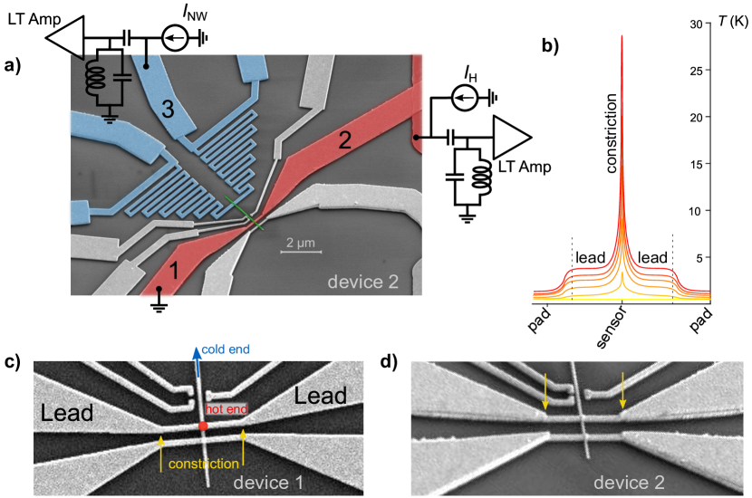
In our experiment we use two types of devices of identical planar architecture shown in the SEM image of Fig. 1a. Single InAs nanowire, emphasized with green color, was deposited on the top of substrate. Colored with light-grey, are bilayers deposited by means of e-beam lithography on the substrate, which form ohmic contacts and side gates to the NW (the latter weren’t used throughout this work). In our measurements only the terminals numbered 1-3 were used while the others were floating. Reddish metallic strip between terminals 1 and 2, biased with current , serves as the contact heater to the NW. The terminal 2 is connected to the DC external circuit and to the low-temperature amplifier for the average noise measurements, while the terminal 1 is kept grounded (see Fig. 1a). On the opposite side, each NW is connected via the terminal 3 and the bluish meander-shaped strip to the DC measurement circuit and another low-temperature amplifier, in this case for the local noise measurements [8].
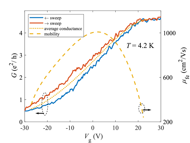
In this work we used devices based on InAs NWs, see fabrication details in ”Materials and Methods”. The high aspect-ratio, the nanometric size and the peculiar electronic transport properties, well known to be diffusive and elastic (energy conserving), make InAs NWs the proper material choice for present experiment. Moreover, the NW resistance falls in a few kOhm range, which is well above the resistances of the connecting metallic terminals and makes InAs a perfect local non-equilibrium sensor [8, 34]. In our experience, these properties are very generic among various types of the InAs NWs, from strongly n-type doped wires grown by chemical beam epitaxy (used in this work) to the undoped catalyst-free wires grown in two different molecular beam epitaxy machines. Fig. 2 shows the results of low temperature transport characterization of our InAs NWs. In a separate device, nominally identical to those used throughout this work, we estimated transconductance [39] and field effect mobility using the approximate analytical model of Ref. [40]. The maximum mobility attained around zero back-gate voltage is and the corresponding carrier density and mean-free path are about and nm, respectively. The obtained is very similar to defect-free doped NWs grown by the same method [41] and is roughly an order of magnitude smaller as compared to the undoped and defect-free InAs NWs [42]. In addition, the gate voltage traces of Fig. 2 do not exhibit Coulomb blockade-like conductance oscillations usually associated with crystal defects in InAs [42, 43]. This suggests that in our devices is likely limited by the ionized impurity or surface scattering. Still we stress again, that the strength of disorder scattering and the value of the carrier density, are not critical parameters for the performance of InAs NWs as local non-equilibrium sensors in present experiment, unlike the elastic transport mechanism.
.
Important part of our devices is the constriction in the middle of the heater strip, see magnified SEM images in Figs. 1c and 1d. The constriction is represented by a 2 m long and narrow metallic wire, which smoothly evolves into the wide and macroscopically long (m) leads. Figs. 1c and 1d reveal a crucial difference between the two devices: D1 was passed through one-step lithography and, thus, a single 120 nm/10 nm thick layer appears, while two-step lithography for the D2 and another, nominally identical device D3, provided a twice thicker metal in the leads area. This difference appears as an abrupt change in evaporated metal thickness marked by yellow arrows in Fig. 1d. Within each heater strip, the constriction serves as the main heater, whereas the remaining leads represent a non-ideal thermal reservoir, that is the reservoir with a finite resistivity and thermal conductivity. An example of a numerically simulated temperature profile along the heater strip is shown in Fig. 1b for different currents , see section Local vs average heater thermometry: impact of the non-ideal leads for the details. Note that the maximum temperature is achieved in the center of the constriction, where the InAs NW connects to the heater via the ohmic contact of negligible electric and thermal resistance ( vs a few k resistance of the NW).
In the following, we mostly concentrate on the measurements performed in the device D1, except for the measurement of the non-equilibrium electronic energy distribution in the device D3 in section InAs NW as an energy preserving sensor and the experiments reported in section Quantitative strategy for thermal biasing in linear response, where we analyze the role of the leads thickness using the devices D1 and D2. Finally, in the last section we present data from a device of different type, based on Aluminum cross with a tunnel junction in the middle, which is described separately in the text.
InAs NW as an energy preserving sensor
The goal of this section is to summarize the capabilities of a diffusive InAs NW as a sensor of the local temperature [8] and the local energy distribution [27]. This is the only experimental section in which the NW is connected to the external current source and biased with the current , which flows between the terminals 3 and 1 in Fig. 1a. We start from the characterization of the transport regime in the InAs NW measuring its shot noise at a bath temperature K. In Fig. 3a we plot the measured NW noise temperature , where is the noise spectral density and is the differential resistance of the NW as a function of , while .
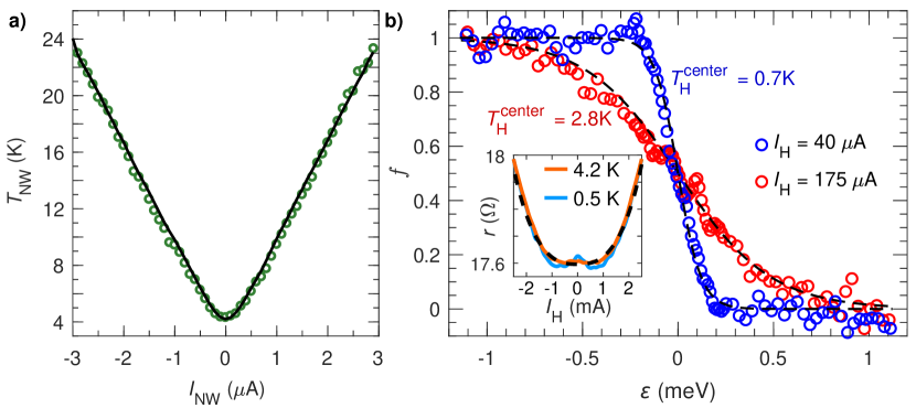
The crossover from the equilibrium Johnson-Nyquist noise at to linear current dependence , where is a Fano factor, is observed and persists up to K (symbols). The theoretical fit (solid line) meets experimental data at which is very close to the universal value for diffusive conductors without electron-phonon relaxation [44, 45]. Thus, a quasiparticle energy is preserved along the NW, making it ideally suited for local noise sensing [8].
As usual in the case of elastic diffusion [44], the electronic energy distribution (EED) at a given location along the NW (in units of its length), , obeys the Laplace’s equation . The solution is a linear combination of the EEDs and given by the external boundary conditions at the two NW ends:
| (2) |
The cold end of the InAs NW (connected to the terminal 3 at ) is always kept in equilibrium with the corresponding EED . In the following we focus on the experiments with a finite heater current , thereby the second boundary condition in the eq. (2) is non-equilibrium. We evaluate the corresponding EED at by utilizing the energy resolved local noise spectroscopy [46, 47]. In this experiment, performed with a separate device nominally identical to D2 at mK, both bias currents and are finite. Also the was chosen high enough, to avoid a problem with the noise analysis caused by a non-linearity of the NW resistance, see Ref. [27] for details. In Fig. 3b the measured is shown for two different values along with the corresponding fits at the same bath temperature (symbols and dashed lines, respectively). The measured is indistinguishable from the Fermi-Dirac EED , where is the temperature of the NW’s hot end, which coincides with the local temperature in the center of the metallic heater constriction. Note that as soon as the EEDs at the NW’s ends are known, there is a unique correspondence between the measured and the , since , see Ref. [44].
The observation of the locally equilibrium EEDs in Fig. 3b implies strong thermalization of the charge carriers in the metallic heater constriction, even at relatively low temperatures of mK and K. This is in contrast to a naive expectation of a double-step EED generated by the current [26]. We believe that the reason for such a strong thermalization is the electron-electron collisions in presence of a spin-flip scattering [48, 49, 50, 47]. In our case such scattering is inevitable owing to the ferromagnetic Ni layer used in metallization. An independent signature of the spin-flip scattering comes from a zero-bias Kondo-like peak observed in a non-linear heater resistance in dependence of at K, see the blue curve in the inset of Fig.3b.
Local vs average heater thermometry: impact of the non-ideal leads
In this section we discuss the impact of the non-ideal leads of the metallic heater constriction on the thermal biasing. Here we supplement the local noise thermometry [8], which provides the knowledge of the temperature at the NW contact position, i.e. at the center of the metallic constriction, with the conventional average noise thermometry [36, 38, 7, 51, 52]. The latter approach is utilized via a measurement of the current noise of the heater strip as a whole, which is picked-up by the low-temperature amplifier at terminal 2. The measured signal in this case is the average noise temperature , which is given by the average of position-dependent heater temperature with the weight of local Joule heat [53]. The difference between the and , along with the spatial temperature distribution in the heater at K and mA, is demonstrated in the inset of Fig. 4a. In the body of Fig. 4a we plot the measured temperature in the center of the metallic constriction against the bias current at K and K (symbols). At , obviously, , while at increasing the measured temperature passes to the linear dependence up to K. As shown in Fig. 4b, the heater-averaged temperature behaves similarly, also demonstrating a linear dependence on the bias current at large enough (symbols). In this case, however, the measured temperature increase is considerably smaller. Such a strong discrepancy between the local and average temperatures highlights the main feature of our heater geometry, which is designed as a macroscopic metallic strip with a short constriction, see Fig. 1.
In Fig.4c we plot the in dependence of the (symbols), and compare the experimental results with the two limiting cases expected in a homogeneous conductor without constriction (dashed lines). Although the spatial temperature profiles are different in the case of a diffusion cooled conductor, sketched next to the upper dashed line, and in the case of the electron-phonon (e-ph) cooled conductor, sketched next to the lower dashed line, in both cases one obtains . By contrast, in our experiment , which is a direct consequence of our heater design. As we discuss below, the constriction and the leads in our case are in the regimes of diffusion cooling and e-ph cooling, respectively, the corresponding temperature profiles are sketched in Fig. 4c.
The solid lines in Figs. 4a, 4b and 4c represent the results of numerical calculations used to fit the experimental data and characterize the parameters of the e-ph cooling in our devices. The underlying physics is captured by the heat balance equation:
| (3) |
where is the Wiedemann-Franz heat conduction of the electronic system, which is responsible for the diffusion cooling mechanism in the heater and is the local current density in the heater. The first term on the rhs of the eq. (3) accounts for the Joule heat production in the heater, whereas the second term stands for the e-ph cooling, both per unit volume. The best fits, capable to explain the data of in Figs. 4a, 4b and 4c up to mA are obtained with the following parameters. First, we assumed the power-law e-ph cooling with and the exponent of . This unusual exponent both provides the best fit to the experimental data in constrictions and is consistent with an independent e-ph cooling measurement in a homogeneous heater, as described below. Second, we took the -dependence of the heater conductivity into account via , where is measured at and is the position-dependent electronic temperature in the heater. The value of the parameter is consistent with the observed dependence of the total heater resistance at K, see the inset of Fig. 3b, and captures the main trend at K.
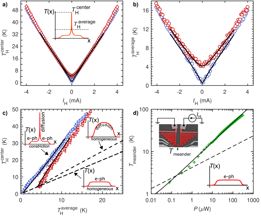
An independent study of the e-ph cooling power is achieved via a measurement of the local temperature in the center of a long meander-shaped heater, depicted in the inset of Fig. 4d. We choose the meander for its length of m, which is significantly longer than e-ph relaxation length (see below). Hence, we expect a flat temperature profile along the meander, such that the measured local temperature is the same as the electron temperature everywhere else in the meander. Fig. 4d shows the measured temperature vs dissipated power at K. The data (symbols) crosses to the power-law behavior, which is best described by and (solid line), which is pretty close to the value of used in our numerical calculations. Again, the exponent of is unusual and is much smaller than the conventional value of observed on a sapphire [6] and oxidized silicon [19] substrates at sub-1K temperatures. This indicates that the e-ph cooling at much higher used in our experiment is considerably bottlenecked by the substrate. This bottleneck is very different from the Kapitza resistance, which is caused by the acoustic mismatch at the interface between the metal film and the insulating substrate. The corresponding heat outflow of , where is the area covered by the meander and is taken from Ref. [6], is shown by the dashed line in Fig. 4d. We observe that for K the experimental data lies substantially above the dashed line, illustrating a different and much stronger bottleneck mechanism functioning in this temperature range. On the one hand, this is not too surprising, given the fact [54] that the phonon mean-free path in amorphous rapidly decays as at increasing temperature above 5 K. On the other hand, the presence of such a non-universal bottleneck strongly complicates numerical modeling, emphasizing the need for accurate experimental calibration of the thermal bias in the experiments.
We conclude this section with an estimation of the e-ph relaxation length, which is defined as follows. In a uniform conductor at a small temperature difference decays exponentially in space. In this case the solution of the eq. (3) is , where is the e-ph relaxation length. Using the fit parameters of Figs. 4a, 4b and 4c we obtain m and m, respectively, at K and K in our Ni/Au metallic heaters. This estimate is in very good agreement with the above conclusion that the constriction and the leads of our heaters are, respectively, much shorter and much longer compared to the .
Quantitative strategy for thermal biasing in linear response
In Fig. 5a we plot the temperature in the center of the heater constriction measured via local noise thermometry in dependence of in two devices at K (symbols). The data clearly capture a systematic effect of the thickness of the metallic heater leads, which we express in terms of the number of the 120 nm/10 nm thick Ni/Au bilayers. The is considerably reduced in D2 () as compared to the case of D1 (), which is perfectly consistent with the results of the numerical calculation of the eq. (3) (dashed, dash-dotted and thin solid lines). The thick solid line in Fig. 5a also shows the calculation in the limit of , which corresponds to the idealized situation of the leads with zero electrical and heat resistances. The data of Fig. 5a demonstrate that the experimental data for substantially differ from each other and from the limit, emphasizing that non-ideal leads have a strong impact on the thermal biasing in reasonable experimental configurations.
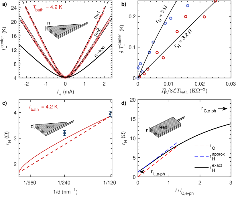
Below we focus on the issue of thermal biasing in the linear response regime, that is in the limit of , where the eq. (3) can be solved analytically. Inspired by the eq. (1), we express the temperature rise in the center of a constriction with a cross-section connected to the leads of a uniform cross-section (see the sketch in Fig. 5d) as follows:
| (4) |
| (5) |
| (6) |
where is the length of the constriction and and are the resistances of a wire with a cross-section of the constriction and the leads, respectively, and the length determined by the corresponding e-ph relaxation length. As follows from the eqs. (4-6), depending on , the interpolates between the solutions with for and with for (see the solid line in Fig. 5d). Both limiting cases correspond to thermal biasing with a uniform metallic strip, for which the effective heater resistance, , is given solely by the a-priori unknown e-ph relaxation length.
The situation is different when the central part of the heater is shaped as a constriction, short compared with the e-ph relaxation length, , which is the case in our experiments. Here, includes the known electrical resistance of the constriction and is given by:
| (7) |
Eq. (7) predicts that the actual value of should vary as a function of both and . This is indeed observed in our experiment, as shown in Figs. 5b and 5c. In Fig. 5b, we plot as a function of the quantity in device D2 at K (blue symbols) and K (red symbols) , along with the fits according to eq. (1). We observe that the initial linear slope of the data for increases at decreasing temperature. This corresponds to the increase of owing to the increased e-ph relaxation length and, thus, of the , see eq. (7). Note the deflection of the blue symbols from the corresponding line at higher currents. Here the measured is not small enough compared to the bath temperature K and the lowest order expansion (4) fails. The higher order correction results in a decrease of the e-ph relaxation length, hence the decrease of the , see Eq. (7), and slowing down of the increase.
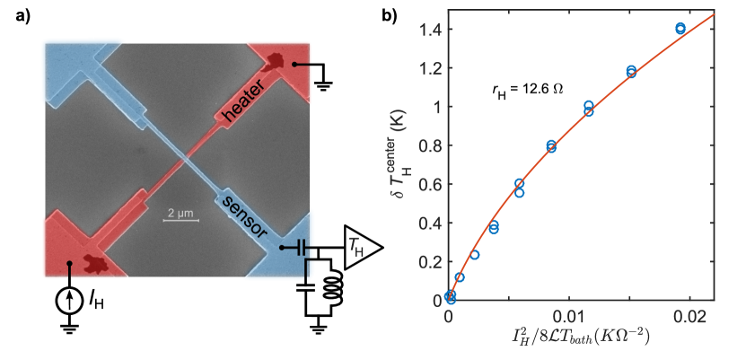
In Fig. 5c we plot the values of in dependence of the inverse thickness of the leads, , obtained in devices D1 and D2 at K (symbols). As seen from the plot, the measured can exceed by about a factor of 2 or more for the chosen device geometry, demonstrating again that the effect of the non-ideal leads is by no means negligible. A strong difference between the and in our experiment is not surprising, for the constriction and leads of the heater are made of the same material and the cross-section area of the leads is still not big enough to make the small. A natural way to minimize the spurious effect of the leads is to make them from a material of much higher conductivity and choose as big as possible. We explored this possibility with a separate device based on an aluminum cross shown in Fig. 6a. Two branches of the cross are connected by a thin tunnel barrier, achieved by in-situ oxidation of the Al. The lower (reddish) branch represents a heater with a 3 m long constriction in the middle. The design of the leads was chosen such that grows quickly away from the constriction and the total lead resistance is small compared to the . The upper (blueish) branch connects the tunnel junction, which plays the role of the local noise sensor in this device, to the low temperature amplifier. The measured local temperature in the middle of the constriction is plotted in Fig. 6b as a function of normalized at K (symbols), along with the best fit to eq. (1). Unlike in our ”careless” NW-based devices, here the lead resistance has a smaller contribution and fitted is much closer to the , see the legend. Correspondingly, the eq. (1) adequately describes the data in a much wider range of as compared to the dataset of Fig. 5b for similar . Moreover, we observed that the device of Fig. 6a supports elastic diffusive transport regime and at even higher the local noise spectroscopy in spirit of Fig. 3b reveals a non-thermal double-step-shaped energy distribution in the center of the heater, see Ref. [47] for details. Obviously, however, this example is special and in most cases the contribution of the leads cannot be made negligible for technical or other reasons. In the following we discuss a strategy for the calibration of the thermal bias in experimentally feasible designs of that kind.
One approach is to make use of a variation of the thickness of the leads in spirit of the present experiment. In this way, using eq. (7) and extrapolating the experimental data (e.g., the TE data) towards one can calibrate the thermal bias quantitatively. Unfortunately, the underlying scaling of with is a-priori unknown and can vary between and , respectively, for the e-ph relaxation scaling with the volume and with the surface of the leads. The latter scaling corresponds to a situation when a bottleneck for the e-ph relaxation occurs via a poor heat conduction of the substrate, which is likely the case in present experiment. The dashed and solid lines in Fig. 5c show the calculated dependencies vs for these two model situations, respectively. In spite of very different functional dependencies, both models are capable to describe the experimental data with roughly the same accuracy, demonstrating how generally challenging it is to use the extrapolation for the calibration of thermal bias. Similarly, one can investigate the dependence of on the , which occurs owing to a variation of the e-ph relaxation via . This approach is also difficult to realize for the underlying temperature dependence is not a-priori known.
The most reliable calibration can be achieved by varying , the length of the constriction, which corresponds to a variation of . In this approach, the contribution of the non-ideal leads remains constant and the uncertainty associated with the features of the e-ph relaxation in the leads becomes irrelevant. The scaling of the effective heater resistance as a function of , in units of the corresponding e-ph relaxation length, is shown in Fig. 5d. This graph is obtained for the parameters of a device similar to our device D1 () at K, but without an intermediate trapezoidal transition region between the constriction and the leads (cf. Fig. 1a). Up to at least , which corresponds to m in our experiment, we observe a sizable dependence of on the length of the constriction, see the solid line in Fig. 5d. This dependence is described by the eqs. (5) and (6) and contains two parameters associated with the e-ph relaxation length in the leads () and in the constriction (). Also shown by the lower dashed line is the resistance of the constriction, , which crosses the dependence at about in this device. Finally, the upper dashed line illustrates the approximation (7), which adequately captures the physics at . Note, that the analytic solution (5-7) is only applicable in a situation when the cross-section of the leads is constant over a few e-ph lengths . In case the shape of the leads is such that varies the trends of Fig. 5d will still hold qualitatively.
We conclude this section by formulating a realistic strategy for a calibration of the thermal bias in a general experiment with non-ideal heaters. We envision an experiment which measures a quantity proportional to the applied thermal bias , such that the evolution of the signal with the length of the heater constriction can be used for the purpose of calibration. The strategy contains the following three steps:
-
•
Design a device with at least two metallic heaters in the form of a narrow constriction of a cross-section connected to the leads of a much larger cross-section . The length of the -th constriction should vary substantially among the heaters. Ideally, should span the range of a few e-ph relaxation lengths, which according to our experiment corresponds roughly to a m scale for Au/Ni metallic bilayer on a substrate at low temperatures.
-
•
Measure the thermal response of the device with respect to all heaters in the linear response regime. For instance, in TE measurements this corresponds to for the -th heater, where is the Seebeck coefficient of the device.
-
•
Fit the experimental functional dependence of on using the eqs. (5) and (6). Use the obtained fit parameters and for the absolute calibration of the thermal bias and, thus, of the or another thermal response in question. We envision that the absolute accuracy of the measurement can be improved to within 10% with such a calibration, instead of about 100% without it.
Summary
In summary, we achieved accurate thermal biasing of a nanoscale electronic device at low temperatures by means of a contact heating approach. Using the average noise thermometry and InAs NW-based local noise sensing we quantified the non-equilibrium electronic energy distribution and the temperature in the center of a metallic diffusive constriction in dependence of bias current. Numerical and analytic calculations allowed us to quantify the heat balance and the role of the non-ideal leads of the heater constriction in the experiment. We presented a simple strategy how to design the metallic heaters capable of generating a predictable thermal bias at nanoscale.
Acknowledgement
We acknowledge valuable discussion with A.I. Kardakova and technical assistance of D. Ercolani. Financial support from the SUPERTOP project, QUANTERA ERA-NET Cofound in Quantum Technologies and from the FET-OPEN project AndQC are acknowledged. Measurements of the local EED in section InAs NW as an energy preserving sensor and numerical calculations were supported by the RFBR project 19-32-80037. Measurements of the local and average noise thermometry were supported by the RSF project 19-12-00326. Analytic calculations in section Quantitative strategy for thermal biasing in linear response were performed under the state task of the ISSP RAS.
Materials and Methods
NW devices were fabricated starting from gold catalyzed n-doped InAs NWs with typical length of 4 m and a diameter 85 nm grown by chemical beam epitaxy [55]. The carrier density of the InAs NWs derived by field effect measurements is about . Typical ohmic contact resistance in our devices is below , whereas the NW resistance is about per micrometer. The metallic nanostructures were realized by electron beam lithography (EBL) process involving two stages. First, 280 nm thick PMMA 950 K resist was spin-coated and followed by a soft-bake at C for 90 sec. The sample was then exposed for e-beam (10 kV) writing. Ni/Au (10/120 nm) was deposited via thermal evaporation on the e-beam written pattern for lift-off. Prior to the Ni/Au deposition, the NWs were passivated using an ammonium polysulfide solution, which ensured the formation of low-resistance ohmic contacts. Second, an additional standard EBL process was performed to achieve a precise overlay (with an accuracy ) and intentionally double the Ni/Au thickness, in the lead areas (see Fig. 1d).
We performed most of the measurements in two inserts, with the samples immersed in liquid (at = 0.5 K) or in gas (at ) and placed vertically face down. The EED data of Fig. 3b (body) were obtained in a cryo-free dilution refrigerator, with the sample in vacuum and inside the metallic case. Here, the lowest achievable electronic temperature in equilibrium did not exceed 80 mK, verified via noise thermometry. The shot noise spectral density was measured using home-made low-temperature amplifiers (LTamp) with a voltage gain of about 10 dB, input current noise of and dissipated power of . We used a resonant tank circuit at the input of the LTamp, see the sketch in Fig. 1a, with a ground bypass capacitance of a coaxial cable and contact pads , a hand-wound inductance of and a load resistance of . The output of the LTamp was fed into the low noise 75 dB total voltage gain room temperature amplification stage followed by a hand-made analogue filter and a power detector. The setup has a bandwidth of MHz around a center frequency of MHz. A calibration was achieved by means of equilibrium Johnson-Nyquist noise thermometry. For this purpose we used a commercial pHEMT transistor connected in parallel with the device, that was depleted otherwise.
References
- [1] Dubi Y and Ventra M D 2009 Nano Letters 9 97–101
- [2] Ye L, Zheng X, Yan Y and Di Ventra M 2016 Phys. Rev. B 94(24) 245105
- [3] Snyder G J and Toberer E S 2008 Nature Materials 7 105
- [4] Giazotto F, Heikkilä T T, Luukanen A, Savin A M and Pekola J P 2006 Rev. Mod. Phys. 78(1) 217–274
- [5] Muhonen J T, Meschke M and Pekola J P 2012 Reports on Progress in Physics 75 046501
- [6] Roukes M L, Freeman M R, Germain R S, Richardson R C and Ketchen M B 1985 Phys. Rev. Lett. 55(4) 422–425
- [7] Strunk C, Henny M, Schönenberger C, Neuttiens G and Van Haesendonck C 1998 Phys. Rev. Lett. 81(14) 2982–2985
- [8] Tikhonov E S, Shovkun D V, Ercolani D, Rossella F, Rocci M, Sorba L, Roddaro S and Khrapai V S 2016 Scientific Reports 6 30621
- [9] Menges F, Mensch P, Schmid H, Riel H, Stemmer A and Gotsmann B 2016 Nature Communications 7 10874
- [10] Shi L, Li D, Yu C, Jang W, Kim D, Yao Z, Kim P and Majumdar A 2003 Journal of Heat Transfer 125 881
- [11] Zuev Y M, Chang W and Kim P 2009 Phys. Rev. Lett. 102(9) 096807
- [12] Zuev Y M, Lee J S, Galloy C, Park H and Kim P 2010 Nano Letters 10 3037–3040
- [13] Wu P M, Gooth J, Zianni X, Svensson S F, Gluschke J G, Dick K A, Thelander C, Nielsch K and Linke H 2013 Nano Letters 13 4080–4086
- [14] Roddaro S, Ercolani D, Safeen M A, Suomalainen S, Rossella F, Giazotto F, Sorba L and Beltram F 2013 Nano Letters 13 3638–3642
- [15] Moon J, Kim J H, Chen Z C, Xiang J and Chen R 2013 Nano Letters 13 1196–1202
- [16] Chen I J, Burke A, Svilans A, Linke H and Thelander C 2018 Phys. Rev. Lett. 120(17) 177703
- [17] Seki S, Ideue T, Kubota M, Kozuka Y, Takagi R, Nakamura M, Kaneko Y, Kawasaki M and Tokura Y 2015 Phys. Rev. Lett. 115(26) 266601
- [18] Roura-Bas P, Arrachea L and Fradkin E 2018 Phys. Rev. B 98(19) 195429
- [19] Wang L B, Saira O P and Pekola J P 2018 Applied Physics Letters 112 013105
- [20] Yazji S, Hoffman E A, Ercolani D, Rossella F, Pitanti A, Cavalli A, Roddaro S, Abstreiter G, Sorba L and Zardo I 2015 Nano Research 8 4048–4060
- [21] Doerk G S, Carraro C and Maboudian R 2010 ACS Nano 4 4908–4914
- [22] Weng Q, Lin K T, Yoshida K, Nema H, Komiyama S, Kim S, Hirakawa K and Kajihara Y 2018 Nano Letters 18 4220–4225
- [23] Weng Q, Komiyama S, Yang L, An Z, Chen P, Biehs S A, Kajihara Y and Lu W 2018 Science 360 775–778
- [24] Schmidt D R, Yung C S and Cleland A N 2004 Phys. Rev. B 69(14) 140301
- [25] Gasparinetti S, Viisanen K L, Saira O P, Faivre T, Arzeo M, Meschke M and Pekola J P 2015 Phys. Rev. Applied 3(1) 014007
- [26] Pothier H, Guéron S, Birge N O, Esteve D and Devoret M H 1997 Phys. Rev. Lett. 79(18) 3490–3493
- [27] Piatrusha S U and Khrapai V S 2017 Measuring electron energy distribution by current fluctuations 2017 International Conference on Noise and Fluctuations (ICNF) pp 1–4
- [28] Swinkels M Y, van Delft M R, Oliveira D S, Cavalli A, Zardo I, van der Heijden R W and Bakkers E P A M 2015 Nanotechnology 26 385401
- [29] Zhou F, Moore A L, Bolinsson J, Persson A, Fröberg L, Pettes M T, Kong H, Rabenberg L, Caroff P, Stewart D A, Mingo N, Dick K A, Samuelson L, Linke H and Shi L 2011 Phys. Rev. B 83(20) 205416
- [30] Hochbaum A I, Chen R, Delgado R D, Liang W, Garnett E C, Najarian M, Majumdar A and Yang P 2008 Nature 451 163
- [31] Yazji S, Swinkels M Y, Luca M D, Hoffmann E A, Ercolani D, Roddaro S, Abstreiter G, Sorba L, Bakkers E P A M and Zardo I 2016 Semiconductor Science and Technology 31 064001
- [32] Li D, Wu Y, Kim P, Shi L, Yang P and Majumdar A 2003 Applied Physics Letters 83 2934–2936
- [33] Boukai A I, Bunimovich Y, Tahir-Kheli J, Yu J K, Goddard III W A and Heath J R 2008 Nature 451 168
- [34] Tikhonov E S, Shovkun D V, Ercolani D, Rossella F, Rocci M, Sorba L, Roddaro S and Khrapai V S 2016 Semiconductor Science and Technology 31 104001
- [35] Tian Y, Sakr M R, Kinder J M, Liang D, MacDonald M J, Qiu R L J, Gao H J and Gao X P A 2012 Nano Letters 12 6492–6497
- [36] Steinbach A H, Martinis J M and Devoret M H 1996 Phys. Rev. Lett. 76(20) 3806–3809
- [37] Nagaev K E 1995 Phys. Rev. B 52(7) 4740–4743
- [38] Henny M, Oberholzer S, Strunk C and Schönenberger C 1999 Phys. Rev. B 59(4) 2871–2880
- [39] Cui Y, Duan X, Hu J and Lieber C M 2000 The Journal of Physical Chemistry B 104 5213–5216
- [40] Ford A C, Ho J C, Chueh Y L, Tseng Y C, Fan Z, Guo J, Bokor J and Javey A 2009 Nano Letters 9 360–365
- [41] Iorio A, Rocci M, Bours L, Carrega M, Zannier V, Sorba L, Roddaro S, Giazotto F and Strambini E 2018 Nano Letters 19 652–657
- [42] Schroer M D and Petta J R 2010 Nano Letters 10 1618–1622
- [43] Nilsson M, Namazi L, Lehmann S, Leijnse M, Dick K A and Thelander C 2016 Phys. Rev. B 93(19) 195422
- [44] Nagaev K 1992 Physics Letters A 169 103 – 107
- [45] Beenakker C W J and Büttiker M 1992 Phys. Rev. B 46(3) 1889–1892
- [46] Gramespacher T and Büttiker M 1999 Phys. Rev. B 60(4) 2375–2390
- [47] Tikhonov E S, Denisov A O, Piatrusha S U, Khrapach I N, Pekola J P, Karimi B, Jabdaraghi R N and Khrapai V S 2020 arXiv:2001.07563
- [48] Kaminski A and Glazman L I 2001 Phys. Rev. Lett. 86(11) 2400–2403
- [49] Anthore A, Pierre F, Pothier H and Esteve D 2003 Phys. Rev. Lett. 90(7) 076806
- [50] Göppert G and Grabert H 2001 Phys. Rev. B 64(3) 033301
- [51] Henny M, Birk H, Huber R, Strunk C, Bachtold A, Krüger M and Schönenberger C 1997 Applied Physics Letters 71 773–775
- [52] Larocque S, Pinsolle E, Lupien C and Reulet B 2020 arXiv:2002.10339
- [53] Piatrusha S U, Khrapai V S, Kvon Z D, Mikhailov N N, Dvoretsky S A and Tikhonov E S 2017 Phys. Rev. B 96(24) 245417
- [54] Zeller R C and Pohl R O 1971 Phys. Rev. B 4(6) 2029–2041
- [55] Gomes U P, Ercolani D, Zannier V, Beltram F and Sorba L 2015 Semiconductor Science and Technology 30 115012