Acceptor levels of the carbon vacancy in 4H-SiC: combining Laplace deep level transient spectroscopy with density functional modeling
Abstract
We provide direct evidence that the broad Z1/2 peak, commonly observed by conventional DLTS in as-grown and at high concentrations in radiation damaged -SiC, has two components, namely Z1 and Z2, with activation energies for electron emission of 0.59 and 0.67 eV, respectively. We assign these components to transition sequences from negative- ordered acceptor levels of carbon vacancy (VC) defects at hexagonal/pseudo-cubic sites, respectively. By employing short filling pulses at lower temperatures, we were able to characterize the first acceptor level of VC on both sub-lattice sites. Activation energies for electron emission of 0.48 and 0.41 eV were determined for and transitions, respectively. Based on trap filling kinetics and capture barrier calculations, we investigated the two-step transitions from neutral to doubly negatively charged Z1 and Z2. Positions of the first and second acceptor levels of VC at both lattice sites, as well as occupancy levels were derived from the analysis of the emission and capture data. Published in Journal of Applied Physics 124, 245701 (2018). https://doi.org/10.1063/1.5063773
I Introduction
Owing to many advantages over silicon, silicon carbide (SiC), in particularly its polytype, is becoming a mainstream material for the industry of high-power electronics.(Kimoto, 2015; She et al., 2017) Due to its wide band gap, radiation hardness, high breakdown field and melting point, SiC is also a promising semiconductor for the fabrication of nuclear radiation detectors working in harsh environments, including at high temperature and dense radiation fields.(Ruddy, Flammang, and Seidel, 2009; Garcia et al., 2013; Wu et al., 2017)
SiC-based diodes for radiation detection are highly sensitive to defects that introduce deep carrier traps,(Ruddy, Flammang, and Seidel, 2009) especially to those with large capture cross section for minority carriers which hold the actual impact signal. Point defects in SiC are mainly created during i) semiconductor material growth, ii) device processing by ion-implantation or iii) during operation under radiation conditions.(Choyke, Matsunami, and Pensl, 2004) It is therefore crucial to understand the effects of accumulated radiation damage on the electrical properties of these devices.
In this work we investigate single and double capture/emission processes involving a major recombination center in -SiC, namely the Z1/2 electron trap, by combining space-charge measurements and first-principles calculations. The Z1/2 trap is a prominent defect in -SiC irradiated for instance with electrons or neutrons,(Nagesh et al., 1987; Storasta et al., 2004) and can be observed by conventional deep level transient spectroscopy (DLTS) as a conspicuous peak around room temperature.(Kimoto et al., 1995; Hemmingsson et al., 1997) It is usually present in as-grown material in concentrations in the range - cm-3, and it is strongly anchored to the lattice being stable up to about 1400 °C.(Alfieri et al., 2005; Ayedh et al., 2015; Bathen et al., 2018) Early DLTS experiments by Hemmingsson et al.(Hemmingsson et al., 1998, 1999) assigned Z1/2 to the superposition of two nearly identical Z1 and Z2 negative- defect transitions, each located on a different sub-lattice site. The negative- ordering of levels implies that during the two-electron filling of the defect, the binding energy (trap depth) of the second electron is higher than that of the first one. Hence, during the reverse process, thermal emission of the first electron immediately induces a second emission.
More recently, by connecting electron paramagnetic resonance (EPR) and photo-EPR data with the DLTS results, it was possible to ascribe Z1/2 to transitions involving the carbon vacancy (VC) in -SiC on distinct sub-lattice sites.(Son et al., 2012) Further, since the metastable EPR-active state was found to be the negative charge state, it became clear that the main Z1/2 peak had to be connected to a emission sequence. This is commonly labelled as Z, where the first emission is the rate-limiting step, corresponding to the measured thermal activation energy (). We also note that based on carrier concentration profiles obtained at several temperatures using implanted/annealed samples, Z1/2 cannot be a donor.(Ayedh et al., 2014)
In Ref. Hemmingsson et al., 1998, the reported activation energies for electron emission were eV and 0.52 eV for Z and Z, respectively, while eV and 0.45 eV for Z and Z. It should be noted that negative- defects undergo strong atomic relaxations upon emission/capture of carriers and may show relatively high barriers between different configurations.(Watkins, 1984; Markevich et al., 1997) Hence, activation energies for carrier emission often differ significantly from the values of the thermodynamic energy levels.(Peaker, Markevich, and Coutinho, 2018) The latter are obtained by subtracting a capture barrier from . While it was not possible to measure the temperature-dependence of the cross-sections (and respective barriers) for the first electron capture, the second capture showed barriers of meV and 80 meV for Z1 and Z2, placing the levels at eV and eV, respectively.(Hemmingsson et al., 1998)
Due to resolution limitations,(Lang, 1974; Peaker, Markevich, and Coutinho, 2018) separate emissions from Z and Z cannot not be resolved by conventional DLTS. To surmount this difficulty, activation energies and capture cross sections for Z and Z were estimated by fitting the data to biexponential capacitance transients subject to a fixed ratio between the two components (taken from the amplitude ratio of the first acceptors).(Hemmingsson et al., 1998) Hence, the measurements of the first and second acceptors could not be carried out independently, adding uncertainty to the measured levels.
These issues were partially addressed by some of us by means of high-resolution Laplace deep level transient spectroscopy (L-DLTS),(Dobaczewski, Peaker, and Nielsen, 2004) which allowed the observation of independent emissions from Z and Z.(Capan et al., 2018) This technique had been previously employed in the separation of an analogous set of deeper traps, labelled , and attributed to donor transitions involving the VC defect in -SiC.(Alfieri and Kimoto, 2013) Laplace-DLTS was also successful in the study of E1/E2 traps observed in -SiC samples.(Koizumi et al., 2013) Like Z1/2, E1/E2 shows up as a prominent band in conventional DLTS spectra of as-grown and irradiated material and has been attributed to a carbon vacancy.(Aboelfotoh and Doyle, 1999) Notably, from the Laplace spectra it was demonstrated that the E1/E2 peak had contributions from three traps, namely E1 which showed the highest emission rate, plus two close deeper traps, E2L and E2H, with relatively lower and higher emission frequencies, respectively. The three peaks were assigned to emissions from equivalent defects located on all three sub-lattice sites of the polytype (, and ).(Koizumi et al., 2013)
The assignment of Z1/2 to the carbon vacancy in -SiC has been widely examined by first-principles modeling. While it is consensual that VC introduces two acceptor levels in the upper half of the gap,(Zywietz, Furthmüller, and Bechstedt, 1999; Torpo et al., 2001; Bockstedte et al., 2010; Trinh et al., 2013; Hornos, Gali, and Svensson, 2011; Coutinho et al., 2017) a clear negative- ordering of levels was obtained only when spurious “periodic-charge” effects were neglected and uncorrected defect energies were used.(Zywietz, Furthmüller, and Bechstedt, 1999; Torpo et al., 2001; Bockstedte et al., 2010; Trinh et al., 2013) The most recent calculations which employed hybrid density functionals, besides not suffering from the severe underestimation of the band-gap as displayed by previous local and semi-local calculations, considered periodic-charge corrected energies. From these calculations, a negative- of about eV was obtained for the vacancy at the -site (hereafter referred to as V), while for the -site the -value was marginally positive ( eV).(Hornos, Gali, and Svensson, 2011; Trinh et al., 2013; Coutinho et al., 2017)
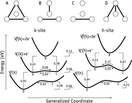
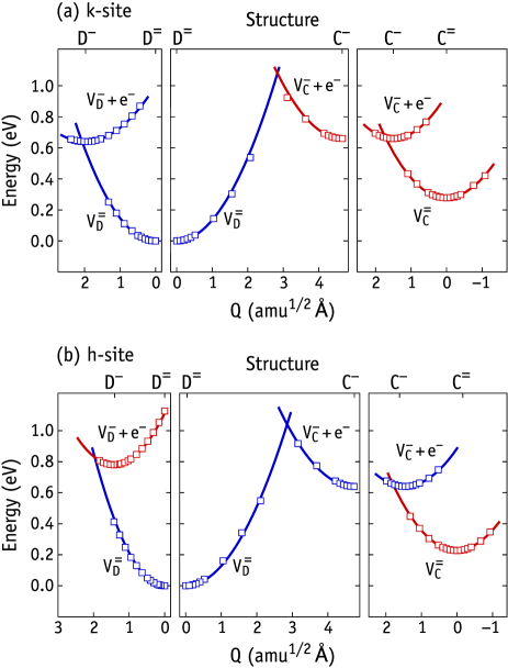
The VC defect displays several structures, depending on the charge state and sub-lattice site.(Trinh et al., 2013; Coutinho et al., 2017) These are denoted as V or V, where is an atomic configuration among those shown in the upper part of Figure 1. The view is along the main axial direction [0001]. The four white circles are Si atoms, three located at basal corners and one at the apex of a triangular pyramid. The missing carbon atom would be located below the Si atom at the apex. Thick lines represent reconstructed bonds formed between the Si radicals. Structure A is the fully symmetric vacancy and it is adopted by the double-plus charge state only. In the lower part of Figure 1 we also depict a calculated configuration coordinate diagram adapted from Ref. Coutinho et al., 2017. Electronic transitions (and respective energies) are indicated by the vertical separation between different minima of the potential curves. For the -site the lowest energy states are V, V and V, while for the -site the most stable structures are V, V an V.
The location of the levels from the hybrid density functional calculations of Ref. Coutinho et al., 2017 are rather close to the Z1/2 levels, i.e., V was predicted to have levels at eV and eV, while V had levels at eV and eV. These transitions correspond to energy differences between the most stable structures for each charge state (see Figure 1). Although the error bar of these calculations is eV, the prediction of a deeper transition of V combined with the more negative -value for V strongly suggests that Z1 and Z2 should be ascribed to V and V, respectively.(Capan et al., 2018)
The goal of the present study is to resolve experimentally the electronic transitions of Figure 1 by means of high-resolution L-DLTS. The capture/emission kinetics and mechanisms, ultimately depend on the activation energies and capture cross-sections. The later are hard to estimate — their calculation involves finding the electron-phonon coupling matrix elements describing a multi-phonon emission process (see Ref. Alkauskas, Yan, and de Walle, 2014 and references therein). Their evaluation is outside the scope of the present work. However, in order to get some insight into the capture/emission mechanims, we calculated approximate values for the capture barriers of several transitions in Figure 1. The paper is organized in the following way: In Section II we describe the experimental and theoretical methodologies, then in Section III we report the conventional and Laplace DLTS data, in Section IV we describe the calculated capture barriers and finally we discuss the results and draw the conclusions in Section V.
II Experimental and theoretical methods
Schottky barrier diodes (SBDs) were produced from epitaxially grown n-type -SiC layers doped with nitrogen (up to cm-3) with µm thickness.(Ito, Storasta, and Tsuchida, 2008) Schottky barriers were formed by evaporation of nickel through a metal mask with patterned square apertures of 1 mm 1 mm, while Ohmic contacts were formed on the backside of the SiC substrate by nickel sintering at 950 °C in Ar atmosphere.
The quality of the SBDs was investigated by current-voltage (-) and capacitance-voltage (-) measurements. A net doping concentration of cm-3 was obtained from the - measurements at 1 MHz and room temperature. Deep level defects were analyzed by means of DLTS and high-resolution L-DLTS to determine their respective activation energies for electron emission and capture cross sections. The DLTS measurements were performed in the temperature range 100-420 K at a ramp rate 3 K/min, reverse bias V, pulse bias V, pulse width ms and using a rate window of 50 s-1.
For the L-DLTS measurements,(Dobaczewski, Peaker, and Nielsen, 2004) capacitance transients were measured with sampling rate, number of samples and number of averaged scans in the range 5-80 kHz, 1200-9000 and 50-3000, respectively. Reverse and pulse biases were respectively V and V. Pulse widths were ms and 100 ns for the and transitions, respectively. The estimated error of the temperature used in the L-DLTS measurements was less than 0.1 K.
For studying the capture kinetics, capacitance transients were measured with different pulse widths in the range - s, while keeping the other parameters constant. In this case, reverse voltage and pulse voltage were respectively V and V. Sampling rate, number of samples and number of averaged scans were in the range 4-80 kHz, 4000-8000 and 600-1500, respectively.
The Fermi level position at the temperature ranges where Z and Z emission peaks were observed was approximately 0.30 eV and 0.22 eV below , respectively. So, in both cases the Fermi level is significantly higher than the occupancy levels of the defects.
For the calculations we employed the Vienna Ab-initio Simulation Package (VASP) code,(Kresse and Hafner, 1993, 1994; Kresse and Furthmüller, 1996) which implements a plane-wave based density functional method. Projector-augmented wave (PAW) potentials were used to describe the core electrons.(Blöchl, 1994) The PAW potentials for Si and C species were generated in the and valence configurations, respectively. We employed the generalized gradient approximation to the exchange-correlation energy as prescribed by Perdew, Burke and Ernzerhof.(Perdew, Burke, and Ernzerhof, 1996) The Kohn-Sham states were expanded in plane-waves with a cut off energy of .
Atomistic models of VC defects were inserted in 400-atom -SiC supercells, obtained by replication of unit cells (using the theoretical lattice parameters Å and Å). We employed a Monkhorst and Pack -point grid to sample the Brillouin zone.(Monkhorst and Pack, 1976) Structural optimization was carried out by means of a conjugate gradient method, with a convergence threshold of eV/Å for the maximum force acting on the nuclei. The self-consistent electronic relaxation cycles were computed with an accuracy of eV.

II.1 Classical capture barriers
Non-radiative capture of free carriers at deep traps often occurs via multi-phonon emission (MPE).(Huang and Rhys, 1950; Kubo and Toyozawa, 1955; Henry and Lang, 1977) Within a classical harmonic picture, MPE capture can be described by means of a configuration coordinate diagram (CCD) as depicted in Figure 2, which refers to the capture of electrons for the sake of convenience. It represents two parabolic potential energy curves, associated with free- () and trapped-electron () states, with respective vibrational mode frequencies and , and energy minima separated by in a generalized coordinate axis. In the energy axis both states are separated by a transition level below the conduction band bottom and they cross at .
MPE transitions take place close to the crossing-point of the two curves at a rate ,(Shockley and Read, 1952; Hall, 1952) which encodes the capture cross section of the trap (), the average thermal velocity of free electrons () and their concentration (). Broadly speaking, the capture cross section for a MPE transition is , where is a purely electronic term that describes the quantum mechanical tunneling rate between free and trapped electron states, while is the often-called “line-shape function” describing the vibrational contribution to the transition rate.(Huang and Rhys, 1950) These terms dominate at low and high temperatures, respectively. In the latter case, the capture process becomes thermally activated as ,(Henry and Lang, 1977) with being the Boltzmann constant and is a capture barrier, i,e., the energy of the CCD crossing point with respect to the potential minimum of the free-electron state.
Obtaining from first-principles is an involved task (see for instance Refs. Shi and Wang, 2012 and Alkauskas, Yan, and de Walle, 2014) which will not be attempted here. Alternatively, we will carry out a comparative analysis of the capture barriers for several transitions displayed in Figure 1. To achieve this we have to make bold assumptions. The first is that the vibronic system can be described by a single effective mode of vibration.(Stoneham, 1981; Makram-Ebeid and Lannoo, 1982) In such a one-dimensional CCD, the relevant parameters are the effective frequencies and , the modal mass and a modal vector connecting the atomic coordinates of atoms of the free- and trapped-electron states, . Here , with and is a Cartesian coordinate of the -th atom.
The second assumption is that the harmonic approximation holds on both states. We define the generalized coordinate as,(Schanovsky, Gös, and Grasser, 2011)
| (1) |
which is obtained from linear interpolation of the coordinates weighted by atomic masses , where is an arbitrary scalar. The units of are amu1/2Å (amu - atomic mass unit). The modal mass
| (2) |
allows us to relate the atomistic distance with the separation in the CCD as . Assuming that the origin of energy and coordinates is at the trapped state, the potential energy close to is,
| (3) |
while near the free-carrier state the potential energy is
| (4) |
where effective frequencies of vibration are obtained as . Finally, the vibronic coupling can by quantified by the Huang-Rhys factor, defined as
| (5) |
which essentially quantifies the number of phonons emitted/created after optical (vertical) luminescence/absorption transitions. Cases where and correspond to weak and strong coupling, and involve small and large defect relaxations, respectively.
Equations 3 and 4 were fitted to first-principles total energy data obtained on a grid of coordinates , between fully relaxed structures in a specific charge state . The calculated energy levels ( in Eq. 4) are those reported in Figure 1. They were calculated using a hybrid density functional method,(Coutinho et al., 2017) which provides accurate energy differences between defects in different charge states. The present semi-local calculations of the harmonic potentials involve relative energies within the same charge state. The use of non-local functionals would not bring significant improvements.
III Experimental results
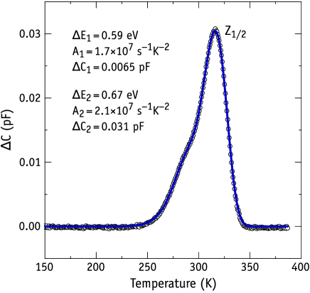
Figure 3 shows a typical DLTS spectrum for as-grown -SiC material. The broad and asymmetric peak with maximum at around 315 K with emission rate 50 s-1 is known as Z1/2, and it was assigned to transitions of VC in -SiC.(Son et al., 2012) Like the E1/E2 peak in -SiC, the asymmetry of the Z1/2 peak of Figure 3 hints a shoulder on the low-temperature side, suggesting the contribution of more than one defect, possibly differing on their sub-lattice sites. The blue solid line in Figure 3 is the simulated DLTS spectrum (for the measurements conditions used) with contributions from two emission signals, the parameters of which have been determined from least-square fitting to the experimental data and are given in the graph. We suggest that the observed emission signals are related to the Z and Z transitions. Further arguments for such assignments are presented below. Concentrations of the Z1 and Z2 traps in the as-grown material studied are estimated to be about cm-3 and cm-3, respectively.
Figure 4 shows high-resolution L-DLTS spectra measured on the same diode for which the conventional DLTS measurements are reported in Fig. 3. The values of the measurement temperature are in the range 325-330 K, i.e. near the temperature of the peak maximum of the Z1/2 DLTS signal. The L-DLTS spectra of Figure 4 clearly show that Z1/2 consists of two close emission components. The results confirm those reported in Ref. Capan et al., 2018, where the high- and low-frequency peaks, namely Z and Z, were ascribed to two-electron emission signals involving V and V, respectively. Positions of the emission components do not change with varying acquisition settings (including numerical methods for the Laplace transform inversion), and therefore it is highly unlikely that the emission signals are related to numerical artifacts, which sometimes in the past were observed in L-DLTS spectra.(Dobaczewski, Peaker, and Nielsen, 2004)
Due to the negative- ordering of the Z1/2 levels, the emission of a second electron follows instantly after the emission of the first one. Hence, from the L-DLTS spectra we only have access to activation energies for the first emission. Peak amplitudes shown in Fig. 4 are proportional to the change in capacitance of the space-charge, and therefore account for both emissions. Hence, the observed two components of Z1/2 relate to and sequential transitions. We note that the labeling of the second acceptors is consistent with that of the first acceptors in Ref. Hemmingsson et al., 1998, where Z and Z were ascribed to the signals with lower and higher amplitudes, respectively.
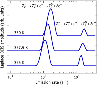
From the L-DLTS peak intensities in Figure 4, we estimate that the concentration ratio is , suggesting that during growth Z2 has higher probability to form, most probably because it is more stable. Previous conventional DLTS studies were not able to directly resolve these two components. The calculated formation energies of the vacancy on both sub-lattice sites indicate that V is more stable than V,(Coutinho et al., 2017) supporting the assignment of Z1 and Z2 to V and V, respectively.
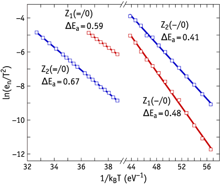
From Arrhenius plots of -corrected electron emission rates, activation energies for Z and Z transitions were determined as 0.59 eV and 0.67 eV, respectively. The Arrhenius fits to the data are shown in Figure. 5. The activation energies compare reasonably well with calculated second acceptor levels at eV for both V and V defects. We should note that this comparison neglects any existing barrier for the capture of electrons. This issue will be addressed below.
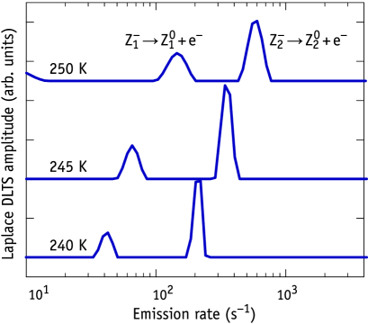
For obtaining information about the shallower Z transitions and confirm the negative- ordering of the acceptor levels, we have applied a procedure similar to that of Ref. Koizumi et al., 2013, which enables to freeze the negatively charged metastable configurations in the sample. Accordingly, we fully emptied the traps by cooling the diode from room temperature down to 220-270 K under reverse bias. The L-DLTS spectra were then recorded by applying a short (100 ns) filling pulse while keeping the number of scans below 50. Such conditions ensures that the number of injected electrons is far too low to double fill the traps, and therefore emissions from double negative defects become small.
Figure 6 shows the L-DLTS spectra of as grown -SiC SBD measured at various temperatures in the range 240-250 K. The measurements were carried out on the same SBD used to obtain the conventional DLTS spectrum shown in Figure 3. In contrast to that spectrum and to the L-DLTS spectra recorded with the application of relatively long (ms range) filling pulses, the use of short pulses leads to the observation of two peaks in the L-DLTS spectra in the temperature range 220-250 K. The two emission signals are assigned to Z and Z transitions based on their relative magnitudes and emission rates. Interestingly, the magnitude ratio is , differing from the value obtained when longer filling pulses were applied and the traps were all double filled. We will return to this issue in Section V, where we will argue that this discrepancy could be due to kinetic effects during the filling pulse. Activation energies for electron emission were determined as 0.48 and 0.41 eV from Arrhenius plots of -corrected emission rates of Z and Z, respectively. These are shown on the right hand side of Figure 5.
We note that the magnitudes of the Z and Z peaks decrease as the number of filling pulses increases, and eventually disappear from the spectra after the application of a relatively large number of filling pulses. This indicates that an increasing fraction of double negatively charged Z1/2 defects form and persist in the sample for the temperature range of the measurements. Such behavior is also a direct evidence for a negative- ordering of the acceptor levels of Z1/2 — the repeated application of filling pulses results in the capture of a second electron by lingering Z defects and therefore in the accumulation of Z defects. The latter will stay in the double minus state, unless the temperature is raised up to room temperature.
As pointed out in Section I, negative- defects show at least two atomic configurations, eventually separated by an energy barrier, and they may as well show considerable barriers for the capture of carriers. This means that activation energies for carrier emission, , may differ significantly from carrier binding energies, , which define the depth of the trap (or a transition level) with respect to edge of the gap (see Figure 2).(Peaker, Markevich, and Coutinho, 2018) Capture barriers and carrier binding energies can be determined from combined emission and capture measurements as a function of temperature.
Besides measuring the activation energies for electron emission for all acceptor levels related to Z1 and Z2, we also carried out direct capture cross section measurements. We found that electron capture by neutral Z1 and Z2 traps is a very fast process. From measurements we could not observed significant changes in magnitudes of the Z and Z emission signals upon varying the length of the filling pulse in the range from 40 ns to 1 µs (in the temperature range 230-260 K). Considering the doping level of our samples, the position of the Fermi level and the shortest length of the filling pulse, we estimated a lower limit for the electron capture cross section of neutral Z1 and Z2 being cm2. These results suggest the existence of a minute or even vanishing capture barrier for both traps. So, it is likely that the depth of the first acceptor levels of Z1 and Z2 with respect to the conduction band bottom are essentially given by the activation energies for electron emission, i.e. they should be located at eV and eV, respectively.
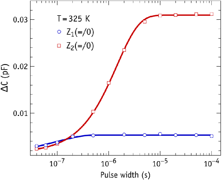
Figure 7 shows how the magnitude of the Z and Z emission signals change with the length of the filling pulse. The data were obtained by L-DLTS at K. For very short pulses ( ns) the number of double filled Z1/2 traps is negligible, while for pulses longer than 10 the signals saturate due to complete double filling. We found that the time-dependence of the signals (measured as capacitance transients of the diode, ) was satisfactorily described by a mono-exponential law
| (6) |
where is the maximum amplitude of the signal and is the characteristic time of the capture transient. is the defect occupancy rate, which for defects in n-type material can be expressed as(Shockley and Read, 1952; Hall, 1952)
| (7) |
where is the electron emission rate, is the electron capture coefficient, and is the concentration of free electrons in the conduction band. The first and the second terms are dominant in Eq. 7 when the Fermi level is below or above the defect occupancy level, respectively. The capture coefficient for defects with U > 0 is expressed as
| (8) |
where is the electron capture cross section, and is the average thermal velocity of free electrons. In general, the capture cross section is a temperature-dependent quantity. For the capture process occurring via multi-phonon emission, the capture cross section can be described by(Henry and Lang, 1977)
| (9) |
where is the barrier for capture, and is the capture cross section at infinitely high temperature.
The occupancy statistics for defects with negative- properties was considered in Ref. Markevich et al., 1997. It was shown that the Eq. 7 is also valid for the defects with , however, with more complicated equations for and . Emission of electrons by a negative- defect with net-charge becomes a dominant process when the Fermi level lies below an occupancy level . For , capture is more effective than emission and therefore,(Markevich et al., 1997)
It was found that in this case, up to four different terms can contribute to , depending on the position of Fermi level with respect to the level and its configurations in the charge state.(Markevich et al., 1997)
When analyzing the capture results presented in Figure 7 we have taken into account the position of the Fermi level with respect to Z and Z defect levels and the configuration structure of VC at and lattice sites in the singly negatively charged states (c.f. Figure 1). It has been concluded that in this case can be expressed as
| (10) |
The solid curves in Figure 7 represent the best fits of Eq. 6 to the Z capture transient data, from which we extracted values of and . Due to its weak magnitude, combined with the sensitivity limits of the equipment, we could not determine the characteristic time of the capture process for Z. According to Eq. 7 a lower limit for the capture cross section of Z was estimated to be cm2, corresponding to a rather small capture barrier. Combining these findings with those above which indicate a vanishing capture barrier for Z as well, we conclude that the depth of the Z trap is essentially the activation energy for electron emission from the double negative charge state, i.e. the level should be at about eV.
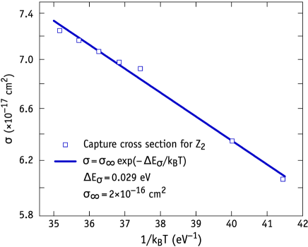
The capture kinetics for Z was measured in the temperature range 300-350K. The Fermi level lies well above the metastable Z level which is estimated at 0.41 eV below the conduction band edge. This ensures that we avoid the formation of singly negative metastable states during the filling pulse. Considering the observed fast capture of electrons by neutral Z2, the thermally activated capture kinetics of Z shown Figure 7 must be limited by the capture of the second electron by singly negative Z defects. These observations also suggest that the geometry of Z1 and Z2 defects should evolve differently along the capture sequence. The temperature dependence of the capture cross section as derived from the experimental data and the use of Eqs. 6 and 10 is presented in Figure 8. The data can be satisfactorily described by Eq. 9, with cm2 and eV. Combining the activation energy for electron emission from double negative Z2 with the electron capture barrier of single negative Z2, we arrive at a Z transition at eV.
| Transition | |||||
|---|---|---|---|---|---|
| Z | |||||
| Z | |||||
| Z | |||||
| Z |
IV Calculation of capture barriers
Now we describe our calculations of the capture barriers for neutral and negatively charged carbon vacancies in -SiC. Figure 1 shows that for neutral VC the capture process departs from V and can in principle arrive either at V or V. For now we are dropping the sub-lattice label ( and ) in the notation of the defect state as in this particular case the picture is analogous for both pseudo-cubic and hexagonal vacancies. Hence, for each sub-lattice site, we have to consider two effective coupling modes, namely and . These were calculated by combining Eq. 1 along with modal vectors and . They connect the end-coordinates of ground-state configurations in charge state (see Section II).
For electron capture by negatively charged vacancies, Figure 1 shows that V and V have close relative energies, particularly for the -site, and are separated by small barriers. We therefore considered C and D initial structures to estimate the capture barriers of vacancies at both - and -sites. Regarding the final state, clearly V is the most stable configuration on both sites, but since V can easily transform to V we also considered capture routes such as . Hence, for the second acceptor, and for both V and V, we have direct-modes and , as well as cross-modes and .
The CCDs where produced by fitting Eqs. 3 and 4 to eleven data points within amu1/2Å around the minimum energy coordinate of each state. Figures 9(a) and 9(b) show calculated CCDs for several transitions involving V and V, respectively. Ground state and metastable configurations are represented in blue and red colors, respectively. Energy differences between different charge states, i.e., the electronic levels, were taken from Ref. Coutinho et al., 2017 and are shown in Figure 1. Besides the data points used for the fittings, additional points were calculated at amu1/2Å to provide us an idea of how much the potential energy deviates from the harmonic regime. The origin of coordinates and energy was assumed at the trapped state, V.
From the fittings, effective mode frequencies in the range cm-1 were obtained. These are consistent with vibrations involving weak Si-Si reconstructed bonds edging the vacancy defects. These frequencies should be compared to 520 cm-1 which is the Raman frequency involving stiffer Si-Si bonds in bulk Si. According to Stoneham,(Stoneham, 1981) the relative positioning of the initial state (before capture) with respect to the final state (after capture) can be described by a coupling ratio,
| (11) |
where is the Huang-Rhys factor, while is the number of phonons spanning the zero-phonon energy. Accordingly, three distinctive situations may occur, (i) which represents the weak coupling limit, where , i.e. the coordinates of both states involved are nearly coincident; (ii) representing a strong coupling case where the potential energy curve of the final state (lower parabola) crosses the initial state (upper parabola) at its minimum energy; (iii) implies that , representing the absurd limit where initial and final states become infinitely distant in the configurational space. We also note that for and the minimum of the upper parabola falls inside and outside the lower parabola, respectively. Examples of and arrangements are shown respectively on the left and middle insets of Figure 9(a).
In broad terms, for the first capture (), and irrespectively of the lattice site, we found that both and effective modes lead to , and therefore to rather small capture barriers meV. Their height is in line with the weak response of the Z L-DLTS peaks as a function of the pulse time. Taking into account the low transformation barriers that separate ground state structures V and V from metastable V and V respectively (see Figure 1), the above results are unable to decide on any of the two possible capture routes under scrutiny.
For electron capture by the negatively charged V defects, transitions involving direct modes ( and ) also show values near 0.5. Consequently, these modes lead to capture barriers not higher than 50 meV. The calculated data and fitted parabolas are shown on the right and left insets of Figures 9(a) and 9(b) for V and V, respectively.
Unlike the above modal distances ( amu1/2Å) or those involved in the first acceptor ( amu1/2Å), configurations C and D are remote from each other in the configurational space ( amu1/2Å). For that reason, transitions coupled to and cross modes show a large and large barriers are expected. For these transitions we estimated capture barriers of at least 0.4 eV (see for example the middle insets of Figures 9(a) and 9(b)).
V Discussion and conclusions
Before the concluding remarks, we provide a critical view on three pending issues:
Error bars related to the calculated capture barriers — The calculated capture barriers are in some cases of the order of tens of meV. Considering the many approximations involved, the error bars for calculated values are probably of the order of 0.1 eV. While it is possible to conclude that most capture barriers are small (except those involving cross-modes), we will restrain ourselves from drawing quantitative conclusions based on the calculated barriers.
Calculated population ratios — It is known that above 1400 °C vacancies are able to migrate.(Bathen et al., 2018) During the cooling of as-grown crystals, vacancies will freeze as the temperature drops below that threshold with a corresponding thermalized population ratio. At such temperatures the material is intrinsic so that VC defects will essentially adopt the neutral charge state. Taking into account the calculated energy difference between V and V of 0.13 eV (see Figure 1), from Boltzmann statistics we obtain a , i.e., almost half of the experimental value reported in Section III from emissions by Z defects. A 4.4 ratio would be obtained at 1400 °C only if V was more stable than V by 0.2 eV. Considering that (i) the population ratio in the sample may not even reflect thermodynamic equilibrium conditions, (ii) the error bar for the calculated formation energies is at least 0.1 eV and (iii) configurational and vibrational entropy should be very similar for analogous defects at and sites, we must conclude than any quantitative account for the observed population ratio by the current theory level is highly speculative.
Different Z1:Z2 amplitude ratios for first and second acceptors — We must consider the possibility that the amplitude ratio [Z:[Z] for the first acceptor (Figure 6) could reflect a flawed [Z:[Z2] population ratio. First we note that both neutral Z1 and Z2 have almost vanishing capture barriers. That leaves us with a capture kinetics dominated by the quantum mechanical tunneling probability at the transition state, which is embodied by the direct capture cross section. Table 1 shows that Z1 traps have larger capture cross sections than Z2. Hence, during a very short filling pulse, the formation of Z will be favored in detriment of Z. This could result in a deceiving [Z]:[Z] ratio which under-estimates the true [Z2]:[Z1] concentration ratio obtained from Z transitions (Figure 4).
If Z and Z are in fact V and V defects which differ in their second neighboring ligands only, one wonders why do they show such different capture cross sections? A possible reason can be found not only in the vacancy states, but in the localization of the lower conduction band states of -SiC. From inspection of the local density of states (LDOS) of bulk -SiC close to the conduction band minima and from plots of , we found that the localization is mostly found on Si()-C() dimers, and nearly vanishes on Si()-C() dimers. Since V is edged by three Si() atoms and one Si() radicals, we expect a larger overlap between the acceptor states of V and the conduction band minimum states. On the other hand, V has only one Si() and three Si() radicals, resulting in a defect with lower capture cross section than V. These arguments not only support the above arguments regarding the capture kinetics, but also support the assignment of Z1 and Z2 to the carbon vacancy at the and lattice sites.
Now we compare the electronic properties of Z1/2 with those of the carbon vacancy in -SiC. We found that both Z1 and Z2 show a negative- ordering for the acceptor levels. Z2 has the larger correlation energy ( eV) with levels at eV and eV, while Z1 has levels separated by only eV and they are located at eV and eV, both lying right between Z and Z . In fact, both Z and Z occupancy (thermodynamic) levels coincide at eV, i.e. at mid-way between their respective metastable acceptors. These results agree well with the most recent calculations,(Hornos, Gali, and Svensson, 2011; Coutinho et al., 2017) where occupancy levels for V and V were estimated at eV and eV, but more significantly V showed a negative eV, while V had a marginally positive eV, supporting direct connections between Z1/2 and V, respectively.
Before discussing the mechanisms for electron capture it is important to note that EPR confirms that negatively charged V and V defects show D and C ground state structures, respectively.(Trinh et al., 2013; Coutinho et al., 2017) Alternative V and V configurations are metastable and can easily be converted to the ground states by surmounting energy barriers of the order of 0.1 eV and lower (see Figure 1).
The measurements indicate that the capture barriers for are very small (or even vanishing). The calculated capture barriers were also found to be very small for transitions involving ground state modes and for V and V, respectively, but they suggest as well that transitions through intermediate metastable states V and V have small capture barriers. From those configurations, a final conversion to ground state structures is only limited by very small transformation barriers. Hence, although it is reasonable to assume mechanisms involving direct transitions between ground states,
we actually cannot rule out the involvement of metastable states.
Regarding the capture of a second electron, we find that Z and Z behave differently, with the former essentially showing a vanishing capture barrier, while for Z we could obtain a small but measurable barrier of eV. The calculations also anticipate a different mechanism for the second capture by the vacancy at the - and -sites. While in Figure 9(a) the capture by V involving ground state structures (blue lines) show a very small capture barrier, the analogous transition involving ground state structures for V is shown in the middle inset of Figure 9(a), and clearly results in a large barrier. Alternatively, we suggest that the transition takes place, firstly via electron capture coupled to , which shows a minute barrier (right inset of Figure 9), quickly followed the transformation towards the ground state V over a barrier which was calculated to be as low as 0.04 eV (see left side of Figure 1). Hence, for the second capture we find,
To conclude, we presented a joint experimental and theoretical investigation of the electronic properties of Z1/2 traps in -SiC. The study addressed the location of individual and transitions in the band gap, as well as the capture and emission dynamics involving these traps. The experiments were carried out by conventional and high-resolution L-DLTS, whereas the calculations employed a plane-wave based density functional theory method using a semi-local approximation to the exchange-correlation energy. We were able to confirm the connection between the levels of Z1 and Z2 with those of the carbon vacancy at the hexagonal and pseudo-cubic sites of the lattice, respectively. We also report direct capture cross section measurements for the levels. These show minute (or vanishing) capture barriers, confirming the calculated strong coupling between initial and final states involved in the transitions. Based on the calculated capture and transformation barriers, detailed mechanisms were proposed for the first and second electron capture.
Acknowledgements
This work is supported by the NATO SPS programme, project number 985215. J.C. thanks the Fundação para a Ciência e a Tecnologia (FCT) for support under project UID/CTM/50025/2013, co-funded by FEDER funds through the COMPETE 2020 Program. I.C. acknowledges financial support from the European Union through the Regional Development Fund for the “Center of Excellence for Advanced Materials and Sensing Devices” (Grant No. KK.01.1.1.01.0001), the European Union’s Horizon 2020 Research and Innovation Programme under grant agreement No. 669014, and the European Union through the European Regional Development Fund – The Competitiveness and Cohesion Operational Programme (Grant No. KK.01.1.1.06). The work in Manchester has been funded by the UK EPSRC under contract EP/P015581/1.
References
- Kimoto (2015) T. Kimoto, Japanese Journal of Applied Physics 54, 040103 (2015).
- She et al. (2017) X. She, A. Q. Huang, O. Lucia, and B. Ozpineci, IEEE Transactions on Industrial Electronics 64, 8193 (2017).
- Ruddy, Flammang, and Seidel (2009) F. H. Ruddy, R. W. Flammang, and J. G. Seidel, Nuclear Instruments and Methods in Physics Research Section A 598, 518 (2009).
- Garcia et al. (2013) T. R. Garcia, A. Kumar, B. Reinke, T. E. Blue, and W. Windl, Applied Physics Letters 103, 152108 (2013).
- Wu et al. (2017) J. Wu, Y. Jiang, M. Li, L. Zeng, J. Li, H. Gao, D. Zou, Z. Bai, C. Ye, W. Liang, S. Dai, Y. Lu, R. Rong, J. Du, and X. Fan, Review of Scientific Instruments 88, 083301 (2017).
- Choyke, Matsunami, and Pensl (2004) W. J. Choyke, H. Matsunami, and G. Pensl, eds., Silicon carbide: recent major advances, Advanced Texts in Physics (Springer-Verlag, Berlin Heidelberg, 2004).
- Nagesh et al. (1987) V. Nagesh, J. W. Farmer, R. F. Davis, and H. S. Kong, Applied Physics Letters 50, 1138 (1987).
- Storasta et al. (2004) L. Storasta, J. P. Bergman, E. Janzén, A. Henry, and J. Lu, Journal of Applied Physics 96, 4909 (2004).
- Kimoto et al. (1995) T. Kimoto, A. Itoh, H. Matsunami, S. Sridhara, L. L. Clemen, R. P. Devaty, W. J. Choyke, T. Dalibor, C. Peppermüller, and G. Pensl, Applied Physics Letters 67, 2833 (1995).
- Hemmingsson et al. (1997) C. Hemmingsson, N. T. Son, O. Kordina, J. P. Bergman, E. Janzén, J. L. Lindström, S. Savage, and N. Nordell, Journal of Applied Physics 81, 6155 (1997).
- Alfieri et al. (2005) G. Alfieri, E. V. Monakhov, B. G. Svensson, and M. K. Linnarsson, Journal of Applied Physics 98, 043518 (2005).
- Ayedh et al. (2015) H. M. Ayedh, R. Nipoti, A. Hallén, and B. G. Svensson, Applied Physics Letters 107, 252102 (2015).
- Bathen et al. (2018) M. E. Bathen, H. M. Ayedh, L. Vines, I. Farkas, E. Janzén, and B. G. Svensson, in Silicon Carbide and Related Materials 2017, Materials Science Forum, Vol. 924 (Trans Tech Publications, 2018) pp. 200–203.
- Hemmingsson et al. (1998) C. G. Hemmingsson, N. T. Son, A. Ellison, J. Zhang, and E. Janzén, Physical Review B 58, R10119 (1998).
- Hemmingsson et al. (1999) C. G. Hemmingsson, N. T. Son, A. Ellison, J. Zhang, and E. Janzén, Physical Review B 59, 7768 (1999).
- Son et al. (2012) N. T. Son, X. T. Trinh, L. S. Løvlie, B. G. Svensson, K. Kawahara, J. Suda, T. Kimoto, T. Umeda, J. Isoya, T. Makino, T. Ohshima, and E. Janzén, Physical Review Letters 109, 187603 (2012).
- Ayedh et al. (2014) H. M. Ayedh, V. Bobal, R. Nipoti, A. Hallén, and B. G. Svensson, Journal of Applied Physics 115, 012005 (2014).
- Watkins (1984) G. D. Watkins, “Festkörperprobleme 24,” (Springer-Verlag, Berlin, Heidelberg, 1984) Chap. Negative- properties for defects in solids, pp. 163–189.
- Markevich et al. (1997) V. P. Markevich, L. I. Murin, T. Sekiguchi, and M. Suezawa, Materials Science Forum 258-263, 217 (1997).
- Peaker, Markevich, and Coutinho (2018) A. R. Peaker, V. P. Markevich, and J. Coutinho, Journal of Applied Physics 123, 161559 (2018).
- Lang (1974) D. V. Lang, Journal of Applied Physics 45, 3023 (1974).
- Dobaczewski, Peaker, and Nielsen (2004) L. Dobaczewski, A. R. Peaker, and K. B. Nielsen, Journal of Applied Physics 96, 4689 (2004).
- Capan et al. (2018) I. Capan, T. Brodar, Ž. Pastuović, R. Siegele, T. Ohshima, S. ichiro Sato, T. Makino, L. Snoj, V. Radulović, J. Coutinho, V. J. B. Torres, and K. Demmouche, Journal of Applied Physics 123, 161597 (2018).
- Alfieri and Kimoto (2013) G. Alfieri and T. Kimoto, Applied Physics Letters 102, 152108 (2013).
- Koizumi et al. (2013) A. Koizumi, V. P. Markevich, N. Iwamoto, S. Sasaki, T. Ohshima, K. Kojima, T. Kimoto, K. Uchida, S. Nozaki, B. Hamilton, and A. R. Peaker, Applied Physics Letters 102, 032104 (2013).
- Aboelfotoh and Doyle (1999) M. O. Aboelfotoh and J. P. Doyle, Physical Review B 59, 10823 (1999).
- Zywietz, Furthmüller, and Bechstedt (1999) A. Zywietz, J. Furthmüller, and F. Bechstedt, Physical Review B 59, 15166 (1999).
- Torpo et al. (2001) L. Torpo, M. Marlo, T. E. M. Staab, and R. M. Nieminen, Journal of Physics: Condensed Matter 13, 6203 (2001).
- Bockstedte et al. (2010) M. Bockstedte, A. Marini, O. Pankratov, and A. Rubio, Physical Review Letters 105 (2010), 10.1103/physrevlett.105.026401.
- Trinh et al. (2013) X. T. Trinh, K. Szász, T. Hornos, K. Kawahara, J. Suda, T. Kimoto, A. Gali, E. Janzén, and N. T. Son, Physical Review B 88, 235209 (2013).
- Hornos, Gali, and Svensson (2011) T. Hornos, A. Gali, and B. G. Svensson, Materials Science Forum 679-680, 261 (2011).
- Coutinho et al. (2017) J. Coutinho, V. J. B. Torres, K. Demmouche, and S. Öberg, Physical Review B 96, 174105 (2017).
- Alkauskas, Yan, and de Walle (2014) A. Alkauskas, Q. Yan, and C. G. V. de Walle, Physical Review B 90 (2014), 10.1103/physrevb.90.075202.
- Ito, Storasta, and Tsuchida (2008) M. Ito, L. Storasta, and H. Tsuchida, Applied Physics Express 1, 015001 (2008).
- Kresse and Hafner (1993) G. Kresse and J. Hafner, Physical Review B 47, 558 (1993).
- Kresse and Hafner (1994) G. Kresse and J. Hafner, Physical Review B 49, 14251 (1994).
- Kresse and Furthmüller (1996) G. Kresse and J. Furthmüller, Physical Review B 54, 11169 (1996).
- Blöchl (1994) P. E. Blöchl, Physical Review B 50, 17953 (1994).
- Perdew, Burke, and Ernzerhof (1996) J. P. Perdew, K. Burke, and M. Ernzerhof, Physical Review Letters 77, 3865 (1996).
- Monkhorst and Pack (1976) H. J. Monkhorst and J. D. Pack, Physical Review B 13, 5188 (1976).
- Huang and Rhys (1950) K. Huang and A. Rhys, Proceedings of the Royal Society A: Mathematical, Physical and Engineering Sciences 204, 406 (1950).
- Kubo and Toyozawa (1955) R. Kubo and Y. Toyozawa, Progress of Theoretical Physics 13, 160 (1955).
- Henry and Lang (1977) C. H. Henry and D. V. Lang, Physical Review B 15, 989 (1977).
- Shockley and Read (1952) W. Shockley and W. T. Read, Physical Review 87, 835 (1952).
- Hall (1952) R. N. Hall, Physical Review 87, 387 (1952).
- Shi and Wang (2012) L. Shi and L.-W. Wang, Physical Review Letters 109 (2012), 10.1103/physrevlett.109.245501.
- Stoneham (1981) A. M. Stoneham, Reports on Progress in Physics 44, 1251 (1981).
- Makram-Ebeid and Lannoo (1982) S. Makram-Ebeid and M. Lannoo, Physical Review B 25, 6406 (1982).
- Schanovsky, Gös, and Grasser (2011) F. Schanovsky, W. Gös, and T. Grasser, Journal of Vacuum Science & Technology B, Nanotechnology and Microelectronics: Materials, Processing, Measurement, and Phenomena 29, 01A201 (2011).