Excitonic States in Semiconducting Two-dimensional Perovskites
Abstract
Hybrid organic/inorganic perovskites have emerged as efficient semiconductor materials for applications in photo-voltaic solar cells with conversion efficiency above 20 %. Recent experiments have synthesized ultra-thin two-dimensional (2D) organic perovskites with optical properties similar to those of 2D materials like monolayer MoS2: large exciton binding energy and excitonic effects at room temperature. In addition, 2D perovskites are synthesized with a simple fabrication process with potential low-cost and large-scale manufacture.
Up to now, state-of-the-art simulations of the excitonic states have been limited to the study of bulk organic perovskites. The large number of atoms in the unit cell and the complex role of the organic molecules makes inefficient the use of ab initio methods. In this work, we define a simplified crystal structure to calculate the optical properties of 2D perovskites, replacing the molecular cations with inorganic atoms. We can thus apply state-of-the-art, parameter-free and predictive ab initio methods like the GW method and the Bethe-Salpeter equation to obtain the excitonic states of a model 2D perovskite. We find that optical properties of 2D perovskites are strongly influenced by excitonic effects, with binding energies up to 600 meV. Moreover, the optical absorption is carried out at the bromine and lead atoms and therefore the results are useful for a qualitatively understanding of the optical properties of organic 2D perovskites.
keywords:
Hybrid perovskites, Two-dimensional materials, Excitonic effects, Ab initio simulations, Optical absortion, Bethe-Salpeter Equation1 Introduction
Semiconducting hybrid organic-inorganic perovskites (HOPV) and all-inorganic perovskites (AIP) are key materials for light harvesting and solar cells applications,1, 2, 3, 4, 5 with conversion efficiencies reported above 20%6, 7. Perovskites can also be synthetized in layered, two-dimensional (2D) structures,8, 9 in analogy with the well-known 2D materials like graphene or monolayer MoS2.10, 11 An interesting 2D perovskite is the Ruddlesden-Popper perovskite, defined by the formula An+1BnX3n+1 where is the number of layers and A is usually an organic molecule like CH3NH3PbX3, B stays for lead and X for bromine or iodine.12, 13, 14 They exhibit intense room-temperature photoluminescence, significant flexibility and strong quantum confinement.15, 16, 17
Moreover, monolayer 2D perovskites () have other interesting optical properties similar to those of 2D semiconductors like hexagonal BN or monolayer MoS2.18, 19, 20, 21, 22, 23 We expect a large excitonic binding energy due to the dramatic reduction of the dielectric screening.24, 25 For instance, the reported experimental value of the exciton binding energy is 467 meV for 2D perovskites (monolayer (CH3NH3)2PbI4),26 corroborated with semi-empirical Bethe-Salpeter Equation calculations.27 In 2D perovskites of (C6H13NH3)2PbI4 the exciton binding energy was estimated in 367 meV28. Experiments have also reported an unusual thickness dependence of the exciton characteristics.29, 26
In addition to the remarkable optical and excitonic properties, 2D HOPV have others advantages with respect other 2D materials. For example, optical properties like the absorption or emission can be modulated by the choosing the composition (by exchanging bromine by iodine, or by using tin in place of lead).30, 12, 31 Moreover, using appropriate molecules as spacers is possible to grow few-layer 2D perovskites with a chosen number of layers.31
In general, accurate theoretical description of perovskites requires the use of large unit cells to capture the disorder related to organic cations.32, 33 Most theoretical contributions use density functional theory (DFT) simulations,34 with focus on the electronic and optical properties of bulk HOPV35, 36 and single-crystal perovskites.37 The large number of atoms in the unit cell of organic 2D perovskites makes prohibitive the simulations including many-body effects such as the Bethe-Salpeter equation (BSE) to account for the excitonic effects.27, 38 Only the studies of bulk perovskites with a few atoms in the unit cell permit the use of fully ab initio approaches such as the GW method or ab initio BSE.39 The current alternatives to fully ab initio simulations are semi-empirical atomistic models of the dielectric constant.40 They can investigate large systems very efficiently and provide an useful insight based on solid-state physics concepts, but they lack the accuracy and predictive power of ab initio BSE.41
In spite of the versatility of the atomistic models the computation of the excitonic states within a full ab initio framework is desirable to obtain predictive information. We propose to use a simplified 2D monolayer perovskite structure, in which the use of ab initio approach becomes efficient and reliable. We replace the organic molecule in the 2D perovskite by a cation atom (cesium in our case), obtaining the layered crystal Csn+1PbnBr3n+1, where is the number of layers. The monolayer structure () Cs2PbBr4 is a suitable system to apply state-of-the-art ab initio methods. We can reproduce the conditions of reduced dielectric screening to obtain the excitonic states and to simulate the optical properties.25 Moreover, our ab initio calculations include the spin-orbit interaction,33 necessary to obtain reliable excitonic states, quantitative exciton binding energies, and to describe realistically the optical properties.
We find remarkable excitonic effects on the optical properties of monolayer 2D perovskites, with exciton binding at the order of 0.5 eV, the existence of dark excitons below the optical absorption edge, and a strong anisotropy of the optical response with respect to the light polarization. Moreover, our simplified 2D crystal can also be used to investigate the role of the number of layers or the different chemical composition.
2 Electronic structure
The monolayer of inorganic perovskite Cs2PbBr4 is constructed from the bulk perovskite CsPbBr3,42 as shown in Fig. 1 (a). We isolate a layer of the octahedron compose by six bromine atoms with one lead atom at the center, and encapsulated with cesium atoms, as shown in Fig. 1 (b), resulting in a unit cell of 7 atoms. In the case of bulk, the space and point group symmetry are and , respectively. The monolayer symmetry has space group 4mmm and point group .
The first step of our study is to determine the stability of the monolayer perovskite. We have used the DFT implementation of Quantum Espresso.43 We work within the local-density approximation (LDA) with norm-conserving fully relativistic pseudopotentials.44 We have optimized the crystal structure, by relaxing the in-plane lattice parameter and the interatomic positions. After relaxation the octahedron formed by bromine atoms is elongated out-of-plane (5.88 Å) and compressed in-plane (5.69 Å) and the inter-atomic distances between cesium atoms are also reduced (from 5.74 to 5.22 Å). The charge density is calculated with a -sampling of , energy cutoff of 100 Ry, and a vacuum distance of 18 Å. Afterwards we have calculated the phonon modes in the relaxed structure. All phonons have positive frequencies and therefore the structure is stable (see phonons band structure in Fig. S2 of the supporting information).
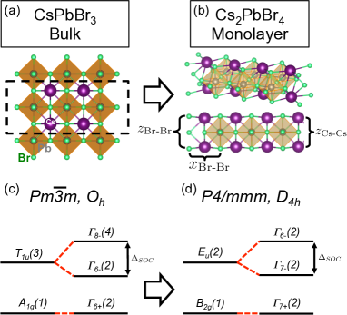
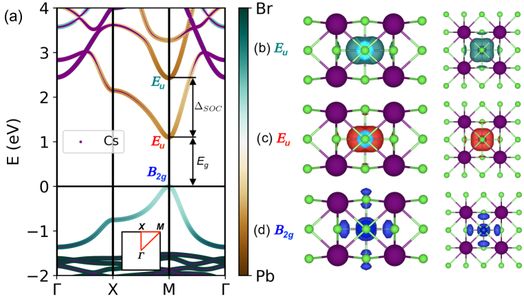
We have calculated within the LDA the band structure of monolayer perovskite, as shown in Fig. 2(a). The inclusion of the spin-orbit interaction is fundamental for a proper description of the band structure of perovskites and therefore we work with full spinorial wave functions (comparison of the band structure obtained with and without the spin-orbit interaction is shown in Fig. S3 of the supporting information).33 The DFT bandgap of monolayer perovskite is located at the point with a value of 1.09 eV. Together with the band structure we have also represented the irreducible representations for bulk and monolayer of the valence band and conduction band states at the bandgap. Figures 2(b), (c) and (d) shows the wave function of the valence and conduction band states at the bandgap at . The spin-orbit interaction has a sizable effect with a splitting 1.33 eV, even larger than the DFT bandgap value, which confirms the necessity of using full spinor wave functions.
In order to make clear the atomic composition of each electronic state, we have projected the wave functions onto the atomic orbitals. In the case of cesium atomic orbitals (purple dots), the dot size corresponds to the relative weight. Alternatively, we have represented the relative weight of the projections onto bromine (green) and lead (brown) atomic orbitals with the color code shown on the color bar, keeping a fixed size. For the electronic states close to the bandgap the electronic density is localized at the bromine and lead atoms, as shown by the weights and the wave function representation, and annotated in Table 1.
Moreover, bands with relevant weight from cesium atomic orbitals are practically decoupled from the bands near , placed mainly at , above 2 eV or at deeper levels around -13 eV (not shown here). The atomic orbital composition of the states close to the bandgap has important consequence on the study of the optical properties. Therefore, from the LDA band structure we conclude that most of the optical activity (like absorption or photoluminescence) is carried out at the bromine and lead atoms. The cations (cesium) enter as a stabilizer of the structure but have lesser impact on the optical properties. Moreover, previous LDA and GW calculations in bulk hybrid perovskites ((CH3NH3)PbI3 and (CH3NH3)SnI3) showed that the electronic structure close to the bandgap is barely affected by the molecular cations.45, 46 Our calculations of the electronic structure of bulk (CH3NH3)PbBr3 and CsPbBr3 shows also that the bands close to the bandgap are very similar in both cases (see Figs. S4 and S5 of the supporting info). Thus, we can expect that the substitution of the cesium cations by molecular cations (like methylammonium) in this 2D material might not change substantially the bands close to the bandgap and therefore the conclusions extracted for the optical properties of monolayer Cs2PbBr4 can be extrapolated to others semiconducting 2D perovskites like (CH3NH3)2PbBr4.
| Wave function | IR | IR-spin | Br | Pb |
|---|---|---|---|---|
| CB | Eu | 13.9 | 82.4 | |
| 17.9 | 79.6 | |||
| VB | B2g | 66.6 | 32.4 |
In addition we have corrected the inherent bandgap underestimation obtained by the DFT-LDA calculations. We have corrected the LDA eigenvalues using the GW method, as implemented in the Yambo code.47, 22, 48 The bandgap correction of G0W0 is 1.61 eV resulting in an electronic bandgap of 2.71 eV. The GW correction of the conduction bands is basically a rigid shift. In the case of the valence band states the GW correction shows a deviation with respect to the rigid shift correction. Therefore, the GW correction has to be applied to all the electronic states considered to calculate the optical properties. (see full GW band structure in Fig. S1 of the supporting information). There are alternatives approaches to the use of GW approximation in perovskites. For instance, the DFT method can calculate the electronic structure with similar accuracy and is computationally more efficient 49. Nevertheless, the goal of this work is to obtain the excitonic states. The BSE and the GW method are both formulated within the same approach, the many-body perturbation theory, and for the size of our system they are still computationally efficient, accurate and parameter-free.
3 Optical Spectra
Once we have determined the electronic structure of the monolayer Cs2PbBr4 we calculate the optical spectra including excitonic effects. We use the Bethe-Salpeter equation (BSE) with full relativistic spin-orbit as implemented in the Yambo code.47 The electron and hole energy eigenvalues are obtained from the GW method and we use the wave functions from the LDA results, calculated in previous Section.47 The vacuum distance between periodic images is 18 Å. We use the Coulomb cutoff technique in the GW and BSE calculations to avoid artificial interaction between periodic images of the layer (more details of the BSE formulation can be found in the first section of the supporting information).50
Figure 3(a) shows the main excitonic states. We have represented the dark exciton , the first two bright excitons for light polarized along ( and ) and ( and ) directions, together with the electronic bandgap, obtained using the GW approximation. The exciton binding energies for the three lowest states are very similar (see Table 2). The dark exciton is at 2.04 eV, 20 meV below (located at 2.06 eV) and 31 meV below (located at 2.071 eV). The excited state excitons and exhibit a smaller binding energy in comparison with and (0.22 eV). The binding energies of 2D perovskites are much larger than in the case of the bulk. The BSE calculations for bulk CsPbBr3 give a binding energy of 68 meV (see BSE spectra in Fig. S6 of the supporting information). The exciton binding energy of bulk is in agreement with previous ab initio BSE calculations performed for CH3NH3PbBr3, which obtained an exciton binding energy of 71 meV51.
In order to verify the composition and symmetry of the excitonic states we have represented the exciton wave functions in the reciprocal -space (see first section of the supporting information for definitions). Figure 3(d) and (e) shows for excitons and . The weights of excitons and are very similar to the one of and they are not represented. In all the cases the weight is localized around the point, at the direct bandgap. The excitonic weights confirm that the optical activity is carried out by wave functions localized at the bromine and lead atom, in agreement with the calculations of the electronic structure. Therefore, in a first approximation, we can neglect the role of the cations, either organic or inorganic, to delve into the optical properties of monolayer perovskites.
The absorption spectra gives a more complete picture of the optical properties. Figures 3(b) and (c) shows the optical spectra of monolayer Cs2PbBr4, obtained at the independent particle approximation (IP, dashed lines) and at the BSE level (solid lines). We represent the absorption for two configurations of light polarization, (b) along (lines in red) and (c) along (lines in green). The spectra are obtained by choosing a Lorentzian width of 75 meV. As expected, the intensity of the spectra is much larger than the one of the due to the depolarization effects.52 In both cases we have a strong renormalization of the IP spectra due to the excitonic effects and the brightest peaks are associated to the and excitons.
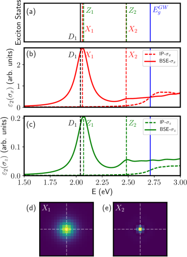
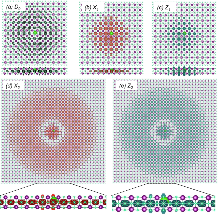
In addition to the -space plots, the real space representation gives further information regarding the localization and symmetry of the excitons. As we have mentioned, only from the -space plots for excitons , and is difficult to highlight the differences between these states. Figure 4(a), (b) and (c) shows the electronic density of the states , and , respectively. In order to analyze the exciton symmetry, we have placed the hole near the bromine atom. From the symmetry analysis of the excitons wave functions we assign the representation to the exciton. Therefore, does not couple to either in-plane light () or out-of-plane light (). Another feature of the excitons is that electronic density is spatially separated from the hole density. This is evidenced by performing BSE calculations without exchange interaction which does not modify the exciton binding energy.
The bright excitons and have and and the selection rules impose coupling to in-plane and out-plane light, respectively. The selection rules can also be deduced from the inspection of their wave functions (in this particular case). If we place the hole near the lead atom, we observe that the density around bromine atoms resemble the shape of atomic orbitals with symmetry for the exciton and with symmetry for the exciton. Moreover, we have represented the excited exciton states and in Fig. 4(d) and (e). These states are much less localized than the first three excitons in accordance with the smaller oscillator strength. They follow the same selection rules that their counterparts and .
| State | |||||
|---|---|---|---|---|---|
| Energy (eV) | 2.040 | 2.060 | 2.071 | 2.479 | 2.482 |
| Binding Energy (eV) | 0.672 | 0.652 | 0.641 | 0.233 | 0.229 |
Our calculations provide some results to be validated by optical experiments. For example, the impact of the dark exciton on the optical properties could be assessed by performing PL as a function of temperature. As summarized in Table 2, the energy separation between and is 20 meV. Thus, increasing population of the exciton in detriment of exciton (by reducing temperature) can affect the PL efficiency. The PL kinetics would also change with temperature because the radiative lifetimes are determined by the exciton oscillator strength and they are different by several order of magnitude between and excitons.53, 54 Moreover, the electron-hole separation observed in the wave function of in Fig. 4 together with the slow radiative recombination can also play an important role in efficient photoinduced charge separation.55 At this respect, magentophotoluminescence experiments can help to elucidate the splitting between and excitons, or the nature of the dark exciton .56
Moreover, our theoretical results is useful to interpret the optical experiments available for organic 2D perovskites of (CH3NH3)n+1PbnBr3n+1 and (CH3NH3)n+1PbnI3n+1.29, 26, 57 The reported values of the exciton binding energy are 467 meV and 490 meV (monolayer (C4H9NH3)2PbI4), against the 652 meV of our calculations.58, 59, 29, 26 In both cases the large value indicates strong excitonic effects, typical of 2D semiconductors. The difference in the value comes from the different dielectric screening. We assume a free-standing monolayer for the calculations while the system of Ref. 26 is surrounded by organic molecules acting as spacers, increasing the dielectric screening and therefore reducing the exciton binding energy.60 Other causes for the deviation are the different bandgap of both systems (1.90 eV in organic perovskite against the 2.71 eV of monolayer perovskite), which can modify the exciton binding energy61, 62 (a comparison with experimental data is shown in Fig. S7 of supporting info). The agreement obtained by the semi-empirical BSE approach developed by Blancon et. al.26 is remarkable, in part thanks to the parabolic dispersion of bands near the bandgap. Nevertheless, the spin-orbit interaction is not included and in systems with a more complicated band structure this model can lose some accuracy.
The relatively simple synthesis of perovskites materials makes possible the fabrication of inorganic 2D materials varying composition. For instance, the replacement of lead by tin and bromine by iodine or chlorine opens the way to change the bandgap within 1 eV,35 and consequently the exciton binding energy. Moreover, the synthesis of nanoplatelets point towards a feasible manipulation of the number of layers.63 In future works, we plan to study the optical properties of 2D perovskites for different chemical compositions and as a function of the number of layers. The synthesis of 2D inorganic perovskites together with the use of molecule as spacers can make possible the growth of colloidal supercells of single-layer perovskites. This single-layer supercell would have a larger optical efficiency due to the larger quantity of active material.38
4 Conclusions
Our approach allows the application of state-of-the-art ab initio simulations like the Bethe-Salpeter equation and the GW method in a simplified model 2D material. We have found a stable 2D perovskite, monolayer Cs2PbBr4, with remarkable excitonic and optical properties. The monolayer shows a direct bandgap at the point and a giant spin-orbit coupling. We have found the excitonic states and classified them in dark and bright excitons. The excitons exhibit a strong exciton binding energy (0.652 eV for the bright exciton).
From the theoretical point of view, simulations in this kind of 2D perovskites are useful to understand the properties of more complex organic 2D perovskites. This system is suitable for more complex simulations, like for instance the study of the electron-phonon interaction to explain non-radiative recombination,64 charge recombination rates65, 54, biexctions66, high-harmonic generation,67 and carrier kinetics.55, 68 So far the synthesis of monolayer Cs2PbBr4 has not been reported but we believe that our work will stimulate efforts addressed toward the synthesis of inorganic 2D perovskites.42 Future works will deal with ab initio approaches to simulate the optical properties of organic 2D perovskites and their dependence on the number of layers.
5 Associated Content
Supporting Information Available: Details of the GW and BSE calculations, phonon band structure, details of the effects of spin-orbit interaction.
6 Acknowledgements
I acknowledge the Juan de la Cierva Program (Grant IJCI-2015-25799) of Spanish Government for its financial support, and my colleagues Juan Martínez-Pastor, Alberto García-Cristóbal, Ludger Wirtz, Fulvio Paleari, and Jacky Even for the reading of the manuscript, and their valuable comments and suggestions.
ASSOCIATED CONTENT Supporting Information Available:
References
- Grätzel 2014 Grätzel, M. The light and shade of perovskite solar cells. Nature Materials 2014, 13, 838–842
- Ahmad et al. 2015 Ahmad, S.; Kanaujia, P. K.; Beeson, H. J.; Abate, A.; Deschler, F.; Credgington, D.; Steiner, U.; Prakash, G. V.; Baumberg, J. J. Strong Photocurrent from Two-Dimensional Excitons in Solution-Processed Stacked Perovskite Semiconductor Sheets. ACS Applied Materials & Interfaces 2015, 7, 25227–25236
- Yettapu et al. 2016 Yettapu, G. R.; Talukdar, D.; Sarkar, S.; Swarnkar, A.; Nag, A.; Ghosh, P.; Mandal, P. Terahertz Conductivity within Colloidal CsPbBr3 Perovskite Nanocrystals: Remarkably High Carrier Mobilities and Large Diffusion Lengths. Nano Letters 2016, 16, 4838–4848
- Frost and Walsh 2016 Frost, J. M.; Walsh, A. What Is Moving in Hybrid Halide Perovskite Solar Cells? Accounts of Chemical Research 2016, 49, 528–535
- Kovalenko et al. 2017 Kovalenko, M. V.; Protesescu, L.; Bodnarchuk, M. I. Properties and potential optoelectronic applications of lead halide perovskite nanocrystals. Science 2017, 358, 745–750
- Bi et al. 2016 Bi, D.; Tress, W.; Dar, M. I.; Gao, P.; Luo, J.; Renevier, C.; Schenk, K.; Abate, A.; Giordano, F.; Correa Baena, J.-P.; Decoppet, J.-D.; Zakeeruddin, S. M.; Nazeeruddin, M. K.; Grätzel, M.; Hagfeldt, A. Efficient luminescent solar cells based on tailored mixed-cation perovskites. Science Advances 2016, 2
- Yang et al. 2017 Yang, W. S.; Park, B.-W.; Jung, E. H.; Jeon, N. J.; Kim, Y. C.; Lee, D. U.; Shin, S. S.; Seo, J.; Kim, E. K.; Noh, J. H.; Seok, S. I. Iodide management in formamidinium-lead-halide–based perovskite layers for efficient solar cells. Science 2017, 356, 1376–1379
- Dou et al. 2015 Dou, L.; Wong, A. B.; Yu, Y.; Lai, M.; Kornienko, N.; Eaton, S. W.; Fu, A.; Bischak, C. G.; Ma, J.; Ding, T.; Ginsberg, N. S.; Wang, L.-W.; Alivisatos, A. P.; Yang, P. Atomically thin two-dimensional organic-inorganic hybrid perovskites. Science 2015, 349, 1518–1521
- Quan et al. 2016 Quan, L. N.; Yuan, M.; Comin, R.; Voznyy, O.; Beauregard, E. M.; Hoogland, S.; Buin, A.; Kirmani, A. R.; Zhao, K.; Amassian, A.; Kim, D. H.; Sargent, E. H. Ligand-Stabilized Reduced-Dimensionality Perovskites. Journal of the American Chemical Society 2016, 138, 2649–2655
- Geim and Grigorieva 2013 Geim, A. K.; Grigorieva, I. V. Van der Waals heterostructures. Nature 2013, 499, 419–425
- Castellanos-Gomez 2016 Castellanos-Gomez, A. Why all the fuss about 2D semiconductors? Nature Photonics 2016, 10, 202–204
- Mao et al. 2018 Mao, L.; Ke, W.; Pedesseau, L.; Wu, Y.; Katan, C.; Even, J.; Wasielewski, M. R.; Stoumpos, C. C.; Kanatzidis, M. G. Hybrid Dion-Jacobson 2D Lead Iodide Perovskites. Journal of the American Chemical Society 2018, 140, 3775–3783
- Stoumpos et al. 2016 Stoumpos, C. C.; Cao, D. H.; Clark, D. J.; Young, J.; Rondinelli, J. M.; Jang, J. I.; Hupp, J. T.; Kanatzidis, M. G. Ruddlesden-Popper Hybrid Lead Iodide Perovskite 2D Homologous Semiconductors. Chemistry of Materials 2016, 28, 2852–2867
- Soe et al. 2018 Soe, C. M. M.; Nie, W.; Stoumpos, C. C.; Tsai, H.; Blancon, J.-C.; Liu, F.; Even, J.; Marks, T. J.; Mohite, A. D.; Kanatzidis, M. G. Understanding Film Formation Morphology and Orientation in High Member 2D Ruddlesden-Popper Perovskites for High-Efficiency Solar Cells. Advanced Energy Materials 2018, 8, 1700979
- Traore et al. 2018 Traore, B.; Pedesseau, L.; Assam, L.; Che, X.; Blancon, J.-C.; Tsai, H.; Nie, W.; Stoumpos, C. C.; Kanatzidis, M. G.; Tretiak, S.; Mohite, A. D.; Even, J.; Kepenekian, M.; Katan, C. Composite Nature of Layered Hybrid Perovskites: Assessment on Quantum and Dielectric Confinements and Band Alignment. ACS Nano 2018, 0, null
- Tsai et al. 2018 Tsai, H.; Asadpour, R.; Blancon, J.-C.; Stoumpos, C. C.; Durand, O.; Strzalka, J. W.; Chen, B.; Verduzco, R.; Ajayan, P. M.; Tretiak, S.; Even, J.; Alam, M. A.; Kanatzidis, M. G.; Nie, W.; Mohite, A. D. Light-induced lattice expansion leads to high-efficiency perovskite solar cells. Science 2018, 360, 67–70
- Blancon et al. 2017 Blancon, J.-C. et al. Extremely efficient internal exciton dissociation through edge states in layered 2D perovskites. Science 2017,
- Splendiani et al. 2010 Splendiani, A.; Sun, L.; Zhang, Y.; Li, T.; Kim, J.; Chim, C.-Y.; Galli, G.; Wang, F. Emerging Photoluminescence in Monolayer MoS2. Nano Letters 2010, 10, 1271–1275
- Hill et al. 2015 Hill, H. M.; Rigosi, A. F.; Roquelet, C.; Chernikov, A.; Berkelbach, T. C.; Reichman, D. R.; Hybertsen, M. S.; Brus, L. E.; Heinz, T. F. Observation of Excitonic Rydberg States in Monolayer MoS2 and WS2 by Photoluminescence Excitation Spectroscopy. Nano Letters 2015, 15, 2992–2997
- Molina-Sánchez et al. 2015 Molina-Sánchez, A.; Hummer, K.; Wirtz, L. Vibrational and optical properties of MoS2: From monolayer to bulk. Surface Science Reports 2015, 70, 554 – 586
- Cassabois et al. 2016 Cassabois, G.; Valvin, P.; Gil, B. Hexagonal boron nitride is an indirect bandgap semiconductor. Nature Photonics 2016, 10, 262–266
- Galvani et al. 2016 Galvani, T.; Paleari, F.; Miranda, H. P. C.; Molina-Sánchez, A.; Wirtz, L.; Latil, S.; Amara, H.; Ducastelle, F. Excitons in boron nitride single layer. Phys. Rev. B 2016, 94, 125303
- Torun et al. 2018 Torun, E.; Miranda, H. P. C.; Molina-Sánchez, A.; Wirtz, L. Interlayer and intralayer excitons in and heterobilayers. Phys. Rev. B 2018, 97, 245427
- Chernikov et al. 2014 Chernikov, A.; Berkelbach, T. C.; Hill, H. M.; Rigosi, A.; Li, Y.; Aslan, O. B.; Reichman, D. R.; Hybertsen, M. S.; Heinz, T. F. Exciton Binding Energy and Nonhydrogenic Rydberg Series in Monolayer . Phys. Rev. Lett. 2014, 113, 076802
- Latini et al. 2015 Latini, S.; Olsen, T.; Thygesen, K. S. Excitons in van der Waals heterostructures: The important role of dielectric screening. Phys. Rev. B 2015, 92, 245123
- Blancon et al. 2018 Blancon, J.-C. et al. Scaling law for excitons in 2D perovskite quantum wells. Nature Communications 2018, 9, 2254–2263
- Pedesseau et al. 2016 Pedesseau, L.; Sapori, D.; Traore, B.; Robles, R.; Fang, H.-H.; Loi, M. A.; Tsai, H.; Nie, W.; Blancon, J.-C.; Neukirch, A.; Tretiak, S.; Mohite, A. D.; Katan, C.; Even, J.; Kepenekian, M. Advances and Promises of Layered Halide Hybrid Perovskite Semiconductors. ACS Nano 2016, 10, 9776–9786
- Tanaka et al. 2005 Tanaka, K.; Takahashi, T.; Kondo, T.; Umebayashi, T.; Asai, K.; Ema, K. Image charge effect on two-dimensional excitons in an inorganic-organic quantum-well crystal. Phys. Rev. B 2005, 71, 045312
- Blancon 2018 Blancon, J.-C. Unusual thickness dependence of exciton characteristics in 2D perovskite quantum wells. arXiv:1710.07653 2018,
- Zhou et al. 2017 Zhou, Z.; Cui, Y.; Deng, H.-X.; Huang, L.; Wei, Z.; Li, J. Modulation of electronic and optical properties in mixed halide perovskites CsPbCl3xBr3(1-x) and CsPbBr3xI3(1-x). Applied Physics Letters 2017, 110, 113901
- Sapori et al. 2016 Sapori, D.; Kepenekian, M.; Pedesseau, L.; Katan, C.; Even, J. Quantum confinement and dielectric profiles of colloidal nanoplatelets of halide inorganic and hybrid organic-inorganic perovskites. Nanoscale 2016, 8, 6369–6378
- Mosconi et al. 2013 Mosconi, E.; Amat, A.; Nazeeruddin, M. K.; Grätzel, M.; De Angelis, F. First-Principles Modeling of Mixed Halide Organometal Perovskites for Photovoltaic Applications. The Journal of Physical Chemistry C 2013, 117, 13902–13913
- Even et al. 2013 Even, J.; Pedesseau, L.; Jancu, J.-M.; Katan, C. Importance of Spin-Orbit Coupling in Hybrid Organic/Inorganic Perovskites for Photovoltaic Applications. The Journal of Physical Chemistry Letters 2013, 4, 2999–3005
- Gebhardt et al. 2017 Gebhardt, J.; Kim, Y.; Rappe, A. M. Influence of the Dimensionality and Organic Cation on Crystal and Electronic Structure of Organometallic Halide Perovskites. The Journal of Physical Chemistry C 2017, 121, 6569–6574
- Huang and Lambrecht 2013 Huang, L.-y.; Lambrecht, W. R. L. Electronic band structure, phonons, and exciton binding energies of halide perovskites CsSnCl3, CsSnBr3, and CsSnI3. Phys. Rev. B 2013, 88, 165203
- Huang and Lambrecht 2015 Huang, L.-y.; Lambrecht, W. R. L. First-principles calculations of phonons and Raman spectra in monoclinic . Phys. Rev. B 2015, 91, 075206
- Park et al. 2015 Park, J.-S.; Choi, S.; Yan, Y.; Yang, Y.; Luther, J. M.; Wei, S.-H.; Parilla, P.; Zhu, K. Electronic Structure and Optical Properties of CH3NH3PbBr3 Perovskite Single Crystal. The Journal of Physical Chemistry Letters 2015, 6, 4304–4308
- Rodríguez-Romero et al. 2017 Rodríguez-Romero, J.; Hames, B. C.; Mora-Seró, I.; Barea, E. M. Conjugated Organic Cations to Improve the Optoelectronic Properties of 2D/3D Perovskites. ACS Energy Letters 2017, 2, 1969–1970
- Filip et al. 2015 Filip, M. R.; Verdi, C.; Giustino, F. GW Band Structures and Carrier Effective Masses of CH3NH3PbI3 and Hypothetical Perovskites of the Type APbI3: A = NH4, PH4, AsH4, and SbH4. The Journal of Physical Chemistry C 2015, 119, 25209–25219
- Giustino et al. 2003 Giustino, F.; Umari, P.; Pasquarello, A. Dielectric Discontinuity at Interfaces in the Atomic-Scale Limit: Permittivity of Ultrathin Oxide Films on Silicon. Phys. Rev. Lett. 2003, 91, 267601
- Even 2015 Even, J. Pedestrian Guide to Symmetry Properties of the Reference Cubic Structure of 3D All-Inorganic and Hybrid Perovskites. J. Phys. Chem. Lett. 2015, 6, 2238–2242
- Rui et al. 2017 Rui, G.; Zhuan, Z.; Abdelaziz, B.; Fang, H.; Alexander, P.; Kai, X.; Jiming, B.; Yan, Y.; Wenzhi, L. Synthesis and Photoluminescence Properties of 2D Phenethylammonium Lead Bromide Perovskite Nanocrystals. Small Methods 2017, 1, 1700245
- Giannozzi et al. 2009 Giannozzi, P. et al. QUANTUM ESPRESSO: a modular and open-source software project for quantum simulations of materials. Journal of Physics: Condensed Matter 2009, 21, 395502 (19pp)
- Lejaeghere et al. 2016 Lejaeghere, K. et al. Reproducibility in density functional theory calculations of solids. Science 2016, 351
- He and Galli 2014 He, Y.; Galli, G. Perovskites for Solar Thermoelectric Applications: A First Principle Study of CH3NH3AI3 (A = Pb and Sn). Chemistry of Materials 2014, 26, 5394–5400
- Brivio et al. 2014 Brivio, F.; Butler, K. T.; Walsh, A.; van Schilfgaarde, M. Relativistic quasiparticle self-consistent electronic structure of hybrid halide perovskite photovoltaic absorbers. Phys. Rev. B 2014, 89, 155204
- Marini et al. 2009 Marini, A.; Hogan, C.; Gr ning, M.; Varsano, D. yambo: An ab initio tool for excited state calculations. Computer Physics Communications 2009, 180, 1392 – 1403
- Sangalli 2018 Sangalli, D. Many-Body perturbation theory calculations using the yambo code. 2018,
- Tao et al. 2017 Tao, S. X.; Cao, X.; Bobbert, P. A. Accurate and efficient band gap predictions of metal halide perovskites using the DFT-1/2 method: GW accuracy with DFT expense. Scientific Reports 2017, 7, 14386–14394
- Rozzi et al. 2006 Rozzi, C. A.; Varsano, D.; Marini, A.; Gross, E. K. U.; Rubio, A. Exact Coulomb cutoff technique for supercell calculations. Physical Review B 2006, 73, 205119
- Bokdam et al. 2016 Bokdam, M.; Sander, T.; Stroppa, A.; Picozzi, S.; Sarma, D. D.; Franchini, C.; Kresse, G. Role of Polar Phonons in the Photo Excited State of Metal Halide Perovskites. Scientific Reports 2016, 6, 28618–28625
- Wirtz et al. 2006 Wirtz, L.; Marini, A.; Rubio, A. Excitons in Boron Nitride Nanotubes: Dimensionality Effects. Phys. Rev. Lett. 2006, 96, 126104
- Palummo et al. 2015 Palummo, M.; Bernardi, M.; Grossman, J. C. Exciton Radiative Lifetimes in Two-Dimensional Transition Metal Dichalcogenides. Nano Letters 2015, 15, 2794–2800
- Chen et al. 2018 Chen, H.-Y.; Palummo, M.; Sangalli, D.; Bernardi, M. Theory and Ab Initio Computation of the Anisotropic Light Emission in Monolayer Transition Metal Dichalcogenides. Nano Letters 2018, 18, 3839–3843
- Liu et al. 2017 Liu, J.; Leng, J.; Wu, K.; Zhang, J.; Jin, S. Observation of Internal Photoinduced Electron and Hole Separation in Hybrid Two-Dimentional Perovskite Films. Journal of the American Chemical Society 2017, 139, 1432–1435
- Robert et al. 2017 Robert, C.; Amand, T.; Cadiz, F.; Lagarde, D.; Courtade, E.; Manca, M.; Taniguchi, T.; Watanabe, K.; Urbaszek, B.; Marie, X. Fine structure and lifetime of dark excitons in transition metal dichalcogenide monolayers. Phys. Rev. B 2017, 96, 155423
- Smith et al. 2017 Smith, I. C.; Smith, M. D.; Jaffe, A.; Lin, Y.; Karunadasa, H. I. Between the Sheets: Postsynthetic Transformations in Hybrid Perovskites. Chem. Mater. 2017, 29, 1868–1884
- Yaffe et al. 2015 Yaffe, O.; Chernikov, A.; Norman, Z. M.; Zhong, Y.; Velauthapillai, A.; van der Zande, A.; Owen, J. S.; Heinz, T. F. Excitons in ultrathin organic-inorganic perovskite crystals. Phys. Rev. B 2015, 92, 045414
- Smith et al. 2017 Smith, M. D.; Pedesseau, L.; Kepenekian, M.; Smith, I. C.; Katan, C.; Even, J.; Karunadasa, H. I. Decreasing the electronic confinement in layered perovskites through intercalation. Chem. Sci. 2017, 8, 1960–1968
- Qiu et al. 2017 Qiu, D. Y.; da Jornada, F. H.; Louie, S. G. Environmental Screening Effects in 2D Materials: Renormalization of the Bandgap, Electronic Structure, and Optical Spectra of Few-Layer Black Phosphorus. Nano Letters 2017, 17, 4706–4712
- Choi et al. 2015 Choi, J.-H.; Cui, P.; Lan, H.; Zhang, Z. Linear Scaling of the Exciton Binding Energy versus the Band Gap of Two-Dimensional Materials. Phys. Rev. Lett. 2015, 115, 066403
- Jiang et al. 2017 Jiang, Z.; Liu, Z.; Li, Y.; Duan, W. Scaling Universality between Band Gap and Exciton Binding Energy of Two-Dimensional Semiconductors. Phys. Rev. Lett. 2017, 118, 266401
- Weidman et al. 2017 Weidman, M. C.; Goodman, A. J.; Tisdale, W. A. Colloidal Halide Perovskite Nanoplatelets: An Exciting New Class of Semiconductor Nanomaterials. Chemistry of Materials 2017, 29, 5019–5030
- Guo et al. 2016 Guo, Z.; Wu, X.; Zhu, T.; Zhu, X.; Huang, L. Electron-Phonon Scattering in Atomically Thin 2D Perovskites. ACS Nano 2016, 10, 9992–9998
- Huang et al. 2017 Huang, J.; Yuan, Y.; Shao, Y.; Yan, Y. Understanding the physical properties of hybrid perovskites for photovoltaic applications. Nature Reviews Materials 2017, 2, 17042–17060
- Thouin et al. 2018 Thouin, F.; Neutzner, S.; Cortecchia, D.; Dragomir, V. A.; Soci, C.; Salim, T.; Lam, Y. M.; Leonelli, R.; Petrozza, A.; Kandada, A. R. S.; Silva, C. Stable biexcitons in two-dimensional metal-halide perovskites with strong dynamic lattice disorder. Phys. Rev. Materials 2018, 2, 034001
- Abdelwahab et al. 2018 Abdelwahab, I.; Grinblat, G.; Leng, K.; Li, Y.; Chi, X.; Rusydi, A.; Maier, S. A.; Loh, K. P. Highly Enhanced Third-Harmonic Generation in 2D Perovskites at Excitonic Resonances. ACS Nano 2018, 12, 644–650
- Molina-Sánchez et al. 2017 Molina-Sánchez, A.; Sangalli, D.; Wirtz, L.; Marini, A. Ab Initio Calculations of Ultrashort Carrier Dynamics in Two-Dimensional Materials: Valley Depolarization in Single-Layer WSe2. Nano Letters 2017, 17, 4549–4555