Temperature dependence of the Seebeck coefficient of epitaxial -Ga2O3 thin films
Abstract
The temperature dependence of the Seebeck coefficient of homoepitaxial metal organic vapor phase (MOVPE) grown, silicon doped -Ga2O3 thin films was measured relative to aluminum. For room temperature we found the relative Seebeck coefficient of V/K. At high bath temperatures K, the scattering is determined by electron-phonon-interaction. At lower bath temperatures between K and K, an increase in the magnitude of the Seebeck coefficient is explained in the frame of Strattons formula. The influence of the different scattering mechanisms on the magnitude of the Seebeck coefficient is discussed and compared with Hall measurement results.
I Introduction
In the past years, -Ga2O3 crystals and thin films have proved to be promising materials for high power devices Stepanov et al. (2016); Suzuki et al. (2007); Green et al. (2016); Chabak et al. (2016); Galazka (2018). However, one drawback is the energy-dissipation, which enhances Joule heating, due to the low thermal conductivityHandwerg et al. (2015, 2016). One approach could be a direct cooling using the Peltier effect.
For this purpose values of the Seebeck coefficient of -Ga2O3 must be known.
-Ga2O3 is a transparent material, with a high band gap eV at room temperatureTippins (1965); Lorenz, Woods, and Gambino (1967); Orita et al. (2000); Peelaers and de Walle (2017); Janowitz et al. (2011).
The majority charge carrier type is n-type and the effective mass has been experimentally determined to be in the order of free electron masses Kang et al. (2017); Mohamed et al. (2011); Janowitz et al. (2011). -Ga2O3 has been intensively studied in terms of charge carrier transport with a maximum mobility so far being cm2/VsGalazka et al. (2014) at room temperature. However, electricalAhrling et al. ; Mitdank et al. (2014) and thermalHandwerg et al. (2015, 2016) conductivity studies remain to be completed by thermoelectric measurements.
In this work we implement a micro lab, based on metallic lines on the homoepitaxially MOVPE grown (100) silicon doped -Ga2O3 thin films and perform temperature-dependent Seebeck measurements between K and K. We compare the results with calculated room temperature Seebeck coefficients based on Hall charge carrier density by using Stratton’s formulaStratton (1962).
II Experimental Details
The thin films have been grown on substrates prepared from Mg-doped, electrically insulating bulk -Ga2O3 single crystals, that were grown along the [010]-direction by the Czochralski methodGalazka et al. (2014, 2016). The substrates with (100)-orientation have been cut with a 6∘ off-orientation to reduce island growthGalazka et al. (2010, 2016) and increase the structural quality of the thin films. The MOVPE process used trimethylgallium and pure oxygen as precursors. Silicon doping has been realized by tetraethylorthosilicate. The substrate temperature was between 750∘C and 850∘C and the chamber pressure between 5 and 100 mbar during growthWagner et al. (2014).
| -Ga2O3 thin film | sample 1 | sample 2 |
|---|---|---|
| high mobility | low mobility | |
| [nm] | 185 | 212 |
| [cm-3] | ||
| [cm2/Vs] | ||
| [cm-3] | ||
| [cm2/Vs] |
The material parameters of the samples are listed in table 1. Both -Ga2O3 thin films have the same magnitude of charge carrier densities but a rather big difference in mobility.
The micro labs have been manufactured by standard photolithography and magnetron sputtering of titanium (7 nm) and gold (35 nm) after cleaning with acetone, isopropanol and subsequent drying. The metal lines of the micro lab are isolated due to a Schottky contact relative to the -Ga2O3 thin film. Ohmic contacts with the -Ga2O3 thin film were achieved by direct wedge bonding with an Al/Si-wire (99/1 %) on the deposited metal structureAhrling et al. , creating point contacts. To keep some parts of the micro lab isolated relative to the thin film, the electrical contacts were prepared by attaching gold wire with indium to the Ti/Au metal lines.
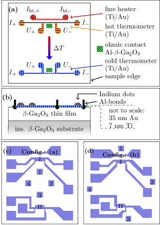
Figure 1 shows the micro lab, that allows the measurement of the Seebeck coefficient, charge carrier density and conductivity.
Figure 1 (a) displays a scheme of the micro lab. It consists of a two-point line heater at the top, were an electrical current is imprinted to create Joule heating, resulting in a temperature gradient across the sample.
Two four-point metal lines close to (hot) and far from (cold) the heater line serve as thermometers. The temperature dependent measurement of their resistances follow the Bloch-Grüneisen-lawTritt (2004) and can be used to calculate the temperature gradient in the area of the four-point resistances.
In this area, Al--Ga2O3 ohmic contacts were placed to measure the thermo voltage.
The experimental procedure involves a measurement of the thermo voltage for as long as it takes to stabilize the temperature gradient across the sample. Afterwards, the four-point resistances of the thermometers are measured. This procedure is repeated for several heating currents before the bath temperature is changed in intervals of 10 K.
Figure 1 (b) illustrates a cross-sectional view of the samples. The Mg-doped electrically insulating -Ga2O3 substrate has been used to grow the Si-doped -Ga2O3 thin film on top thereof. The Ti/Au metal lines of the micro lab have then been deposited on the surface of the thin film and electrical contacts have been prepared either by wedge-bonding with Al-wire (ohmic contact) or attachement of Au-wire with indium (Schottky contact).
Figure 1 (c) and (d) show two different designs (a) and (b) for electrical measurements in the 4-point van-der-Pauw configuration and differences in the 4-point thermometers. In figure 1 (c) the van-der-Pauw contacts (1-4) are located in the centre of the sample.
To check the validity of the measurement setup, an alternative measurement configuration has been developed (measurement configuration (b)).
The measurement configuration (b) is shown in figure 1 (d). Here, the van-der-Pauw contacts are close to the edge of the sample.
The measurement configuration a has been used to investigate the 185 nm thick high mobility sample and one 212 nm thick low mobility sample. To verify that there is no influence because of the van-der-Pauw contacts, a second 212 nm thick low mobility sample has been investigated with the measurement configuration (b).
III Measurement Results
The thermo voltage was measured as a function of temperature gradient for several bath temperatures and -Ga2O3 thin films.
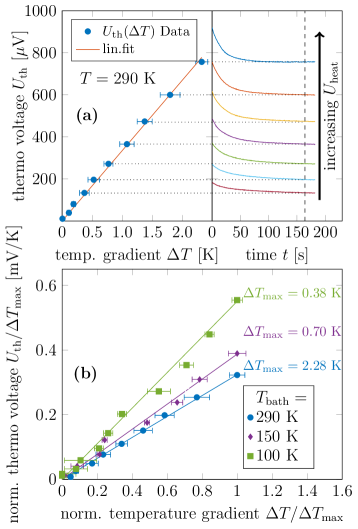
In the right graph of figure 2 (a) the measurements of the thermo voltage as a function of time for different temperature gradients can be seen. The measurements are performed for 180 seconds and the last 10 % of the measured data (marked by the vertical dashed line) are used to evaluate the thermo voltage as a function of temperature gradient (left graph). Due to the weaker thermal conductivity and diffusivity of -Ga2O3 at higher temperaturesHandwerg et al. (2015, 2016), it takes longer to evolve a stable temperature gradient and thermo voltage as compared to lower temperatures.
The left graph of figure 2 (a) shows the thermo voltage as a function of the temperature gradient. These data can be well fitted with a linear equation, where the slope equals the Seebeck coefficient
| (1) |
Figure 2 (b) shows the normalized thermo voltage as a function of normalized temperature gradient for bath temperatures of 290 K, 150 K, and 100 K with substracted offsets for the same sample as figure 2 (a). The change of the Seebeck coefficient as a function of bath temperature can be observed by the change of the slope of the linear fits.
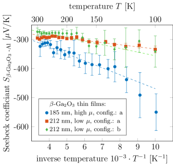
Figure 3 displays the measured Seebeck coefficients of different -Ga2O3 thin films as a function of inverse bath temperature between 100 K and 300 K. The Seebeck coefficients are in the range of V/K to V/K above 100 K. At room temperature, the Seebeck coefficients are V/K for all investigated -Ga2O3 samples. The correction of the Seebeck coefficient due to the aluminum wire is less than . The high mobility -Ga2O3 thin film shows a stronger increase of the Seebeck coefficient for lower temperatures than the low mobility -Ga2O3 thin films. We find, that the investigated measurement configuration has no detectable influence on the Seebeck coefficient. The lower magnitude of the Seebeck coefficient for the 212 nm thick low mobility sample at low temperatures is expected to be due to different charge carrier scattering mechanisms.
These results are similar to those of other transparent conducting oxides like ZnO or In2O3, where Seebeck coefficients in the range from V/K to V/K have been measuredBarasheed, Kumar, and Alshareef (2013); Bierwagen (2015).
IV Discussion
The study of the temperature dependent Seebeck coefficient for -Ga2O3 thin films gives an insight into the scattering mechanisms within the materialYoung et al. (2000); Herring (1954); Ginley (2010). Here we discuss the obtained Seebeck coefficients and their description by the Stratton formula Stratton (1962):
| (2) |
with the elemental charge e, the scattering parameter , the reduced electron chemical potential and the conduction band energy , Fermi energy and Boltzmann constant . The scattering parameter is related to the scattering mechanisms within the sample. A first approximation of formula (2) has been plotted in figure (3). A linear fit with constant and has been performed for K and plotted in figure 3 (dashed lines). For the 185 nm thick high mobility sample meV and for the 212 nm thick low mobility samples meV has been obtained. These different electron chemical potentials explain the different temperature dependencies but only give a rough estimation since and .
To calculate theoretical values for the Seebeck coefficient at room temperature, we use the analytical expression after Nilsson Nilsson (1973), which interpolates the range between non degenerated and degenerated semiconductors. The reduced electron chemical potential is then given by
| (3) |
| (4) |
with beeing the effective density in the conduction band:
| (5) |
With an effective mass of m, which we obtained by fitting the measured temperature dependent charge carrier density with the neutrality equation, and a Seebeck scattering parameter of Ginley (2010); Preissler et al. (2013); Sze and Ng (2007), which applies for electron-phonon scattering we calculated theoretical values using the Stratton formula (2). That calculation yields a value of 250 KV/K,
The measurement of the Seebeck coefficient and charge carrier density allows a calculation of the scattering parameter if the effective mass is known. One has to consider, that the measurement of the charge carrier density using Hall measurements is influenced by the scattering of the free electrical charges as well. This is usually described by the Hall scattering factor Sze and Ng (2007), if the relaxation time can be expressed by :
| (6) |
with being the gamma function, the Hall mobility and the drift mobility.
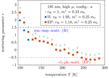
In order to correctly calculate the general scattering parameter one needs to know the Hall scattering parameter or vice versa. Commonly for electron phonon (EP) scattering and for ionized impurity (II) scattering are assumedSze and Ng (2007). This allows a calculation of the scattering parameter , if we assume that only II or EP scattering dominate the charge transport. Figure 4 shows the calculated as a function of bath temperature. The calculations were performed with equation (2) considering the measured Seebeck coefficients and measured charge carrier densities, as well as various Hall scattering factors and effective masses for the 185 nm thick high mobility -Ga2O3 thin film.
For and (open diamonds) no correction of the charge carrier density has been done and the effective mass has been used as obtained from temperature dependent charge carrier densities fits. If we consider Hall scattering factorsSze and Ng (2007) of and for ionized impurity scattering and electron-phonon interaction, respectively, and assume an effective mass of as reported in the literatureJanowitz et al. (2011), we obtain the blue dots and red squares, for II and EP scattering respectively. The obtained results near room temperatures are in agreement with the expected value of for electron-phonon-scattering (figure 4 lower dashed line) Ginley (2010); Preissler et al. (2013); Sze and Ng (2007). For -Ga2O3 thin films electron-phonon-scattering is expected to be the dominant scattering mechanism at these temperaturesAhrling et al. . Here, the scattering mechanism dominating the charge transfer caused by electrical potential gradients is the same as caused by temperature gradients.
For low temperatures we obtain values close to as expected for ionized-impurity scattering (upper dashed line). This is also in agreement with values reported in literatureGinley (2010); Preissler et al. (2013); Sze and Ng (2007). Ionized impurity scattering has been reportedAhrling et al. ; Oishi et al. (2015) to become the dominant scattering mechanism in -Ga2O3 below 100 K, depending on layer thickness and doping. This explains why we obtain values close to 1.5 if we assume that the charge carrier scattering mechanisms influencing the mobility and the Seebeck effect are the same.
The Seebeck coefficients in -Ga2O3 thin films at room temperature are mainly dependent on the doping level, since electron phonon scattering is the dominant scattering mechanism, whereas at low temperatures the different dominant scattering mechanisms have a major impact on the magnitude of the Seebeck coefficient. These observations are consistent with previous studies on thermalHandwerg et al. (2015, 2016) and electrical(Ahrling et al., ; Mitdank et al., 2014) conductivity where the dominant scattering mechanisms at room temperature are phonon-based. For applications at higher temperatures, the room temperature magnitude of the Seebeck coefficient gives an upper limit. Furthermore we can estimate that approaches a value of in the intrinsic regime.
V Conclusion
In conclusion, the temperature dependent Seebeck coefficient of homoepitaxial -Ga2O3 thin films can be explained by the Stratton formula. -Ga2O3 thin films have Seebeck coefficients relative to aluminum of V/K at room temperature with an increase in magnitude at lower temperatures. This leads to a room temperature Peltier coefficient of V. The dependency of the Seebeck coefficent on the dominant scattering mechanism gives the possibility of Seebeck coefficient engineering by growing -Ga2O3 thin films with, for example, an increased concentration of neutral impurities or ionized impurities.
Acknowledgement
This work was performed in the framework of GraFOx, a Leibniz-ScienceCampus partially funded by the Leibniz association and by the German Science Foundation (DFG-FI932/10-1 and DFG-FI932/11-1). The authors thank M. Kockert for fruitful scientific discussions.
References
- Stepanov et al. (2016) S. I. Stepanov, V. I. Nikolaev, V. E. Bougrov, and A. E. Romanov, “Gallium oxide: Properties and application - a review,” Rev. Adv. Mater. Sci. 44, 63–86 (2016).
- Suzuki et al. (2007) N. Suzuki, S. Ohira, M. Tanaka, T. Sugawara, K. Nakajima, and T. Shishido, “Fabrication and characterization of transparent conductive sn-doped -ga2o3 single crystal,” Phys. Stat. Sol. (c) 4, 2310–2313 (2007).
- Green et al. (2016) A. J. Green, K. D. Chabak, E. R. Heller, R. C. Fitch, M. Baldini, A. Fiedler, K. Irmscher, G. Wagner, Z. Galazka, S. E. Tetlak, A. Crespo, K. Leedy, and G. H. Jessen, “3.8-MV/cm breakdown strength of MOVPE-grown sn-doped -ga2o3 mosfets,” IEEE Electron Device Letters 37, 902–905 (2016).
- Chabak et al. (2016) K. D. Chabak, N. Moser, A. J. Green, D. E. Walker, S. E. Tetlak, E. Heller, A. Crespo, R. Fitch, J. P. McCandless, K. Leedy, M. Baldini, G. Wagner, Z. Galazka, X. Li, and G. Jessen, “Enhancement-mode ga2o3 wrap-gate fin field-effect transistors on native (100) -ga2o3 substrate with high breakdown voltage,” Applied Physics Letters 109, 213501 (2016).
- Galazka (2018) Z. Galazka, “-ga2o3 for wide-bandgap electronics and optoelectronics,” Semiconductor Science and Technology 33, 113001 (2018).
- Handwerg et al. (2015) M. Handwerg, R. Mitdank, Z. Galazka, and S. F. Fischer, “Temperature-dependent thermal conductivity in mg-doped and undoped -ga2o3 bulk crystals,” Semiconductor Science and Technology 30, 024006 (2015).
- Handwerg et al. (2016) M. Handwerg, R. Mitdank, Z. Galazka, and S. F. Fischer, “Temperature-dependent thermal conductivity and diffusivity of a mg-doped insulating -ga2o3 single crystal along [100], [010] and [001],” Semiconductor Science and Technology 31, 125006 (2016).
- Tippins (1965) H. H. Tippins, “Optical absorption and photoconductivity in the band edge of -ga2o3,” Physical Review 140, A 316–A 319 (1965).
- Lorenz, Woods, and Gambino (1967) M. R. Lorenz, J. F. Woods, and R. J. Gambino, “Some electrical properties of the semiconductor -ga2o3,” J. Phys. Chem. Solids 28, 403–404 (1967).
- Orita et al. (2000) M. Orita, H. Ohta, M. Hirano, and H. Hosono, “Deep-ultraviolet transparent conductive -ga2o3,” Applied Physics Letters 77, 4166–4168 (2000).
- Peelaers and de Walle (2017) H. Peelaers and C. G. V. de Walle, “Lack of quantum confinement in ga2o3 nanolayers,” Physical Review B 96, 081409 (2017).
- Janowitz et al. (2011) C. Janowitz, V. Scherer, M. Mohamed, A. Krapf, H. Dwelk, R. Manzke, Z. Galazka, R. Uecker, K. Irmscher, R. Fornari, M. Michling, D. Schmeißer, J. R. Weber, J. B. Varley, and C. G. V. de Walle, “Experimental electronic structure of in2o3 and ga2o3,” New Journal of Physics 13, 085014 (2011).
- Kang et al. (2017) Y. Kang, K. Krishnaswamy, H. Peelaers, and C. G. V. de Walle, “Fundamental limits on the electron mobility of -ga2o3,” Journal of Physics: Condensed Matter 29, 234001 (2017).
- Mohamed et al. (2011) M. Mohamed, I. Unger, C. Janowitz, R. Manzke, Z. Galazka, R. Uecker, and R. Fornari, “The surface band structure of -ga2o3,” Journal of Physics: Conference Series 286, 012027 (2011).
- Galazka et al. (2014) Z. Galazka, K. Irmscher, R. Uecker, R. Bertram, M. Pietsch, A. Kwasniewski, M. Naumann, T. Schulz, R. Schewski, D. Klimm, and M. Bickermann, “On the bulk -ga2o3 single crystal grown by the czochralski method,” Journal of Crystal Growth 404, 184–191 (2014).
- (16) R. Ahrling, J. Boy, M. Handwerg, O. Chiatti, R. Mitdank, G. Wagner, Z. Galazka, and S. F. Fischer, “Transport properties and finite size effects in -ga2o3 thin films,” http://arxiv.org/abs/1808.00308v3 .
- Mitdank et al. (2014) R. Mitdank, S. Dusari, C. Bülow, M. Albrecht, Z. Galazka, and S. F. Fischer, “Temperature-dependent electrical characterization of exfoliated -ga2o3 micro flakes,” physica status solidi (a) 211, 543–549 (2014).
- Stratton (1962) R. Stratton, “Diffusion of hot and cold electrons in semiconductor barriers,” Physical Review 126, 2002 – 2014 (1962).
- Galazka et al. (2016) Z. Galazka, R. Uecker, D. Klimm, K. Irmscher, M. Naumann, M. Pietsch, A. Kwasniewski, R. Bertram, S. Ganschow, and M. Bickermann, “Scaling-up of bulk -ga2o3 single crystals by the czochralski method,” ECS Journal of Solid State Science and Technology 6, Q3007–Q3011 (2016).
- Galazka et al. (2010) Z. Galazka, R. Uecker, K. Irmscher, M. Albrecht, D. Klimm, M. Pietsch, M. Brützam, R. Bertram, S. Ganschow, and R. Fornari, “Czochralski growth and characterization of -ga2o3 single crystals,” Crystal Research and Technology 45, 1229–1236 (2010).
- Wagner et al. (2014) G. Wagner, M. Baldini, D. Gogova, M. Schmidbauer, R. Schewski, M. Albrecht, Z. Galazka, D. Klimm, and R. Fornari, “Homoepitaxial growth of -ga2o3 layers by metal-organic vapor phase epitaxy,” Physica Status Solidi (A) 211, 27–33 (2014).
- Tritt (2004) T. M. Tritt, Thermal Conductivity: Theory, Properties, and Applications (New York: Springer, 2004).
- Barasheed, Kumar, and Alshareef (2013) A. Z. Barasheed, S. R. S. Kumar, and H. N. Alshareef, “Temperature dependent thermoelectric properties of chemically derived gallium zinc oxide thin films,” Journal of Materials Chemistry C 1, 4122 (2013).
- Bierwagen (2015) O. Bierwagen, “Indium oxide - a transparent, wide-band gap semiconductor for (opto)electronic applications,” Semiconductor Science and Technology 30, 024001 (2015).
- Young et al. (2000) D. L. Young, T. J. Coutts, V. I. Kaydanov, A. S. Gilmore, and W. P. Mulligan, “Direct measurement of density-of-states effective mass and scattering parameter in transparent conducting oxides using second-order transport phenomena,” Journal of Vacuum Science & Technology A 18, 2978 (2000).
- Herring (1954) C. Herring, “Theory of the thermoelectric power of semiconductors,” The Physical Review 96, 1163–1187 (1954).
- Ginley (2010) D. S. Ginley, Handbook of Transparent Conductors, edited by H. Hosono and D. C. Paine (Springer, New York, 2010).
- Nilsson (1973) N. G. Nilsson, “An accurate approximation of the generalized einstein relation for degenerate semiconductors,” Physica Status Solidi (A) 19, K75–K78 (1973).
- Preissler et al. (2013) N. Preissler, O. Bierwagen, A. T. Ramu, and J. S. Speck, “Electrical transport, electrothermal transport, and effective electron mass in single-crystalline in2o3 films,” Physical Review B 88, 085305 (2013).
- Sze and Ng (2007) S. M. Sze and K. K. Ng, Physics of Semiconductor Devices (Wiley-Interscience, 2007).
- Oishi et al. (2015) T. Oishi, Y. Koga, K. Harada, and M. Kasu, “High-mobility -ga2o3(01) single crystals grown by edge-defined film-fed growth method and their schottky barrier diodes with ni contact,” Applied Physics Express 8, 031101 (2015).
- Víllora et al. (2008) E. G. Víllora, K. Shimamura, Y. Yoshikawa, T. Ujiie, and K. Aoki, “Electrical conductivity and carrier concentration control in -ga2o3 by si doping,” Applied Physics Letters 92, 202120 (2008).
- Matsubara et al. (2001) I. Matsubara, R. Funahashi, T. Takeuchi, S. Sodeoka, T. Shimizu, and K. Ueno, “Fabrication of an all-oxide thermoelectric power generator,” Applied Physics Letters 78, 3627–3629 (2001).
- Ambia, Islam, and Hakim (1992) M. G. Ambia, M. N. Islam, and M. O. Hakim, “Studies on the seebeck effect in semiconducting zno thin films,” Journal of Materials Science 27, 5169–5173 (1992).
- Jood et al. (2011) P. Jood, R. J. Mehta, Y. Zhang, G. Peleckis, X. Wang, R. W. Siegel, T. Borca-Tasciuc, S. X. Dou, and G. Ramanath, “Al-doped zinc oxide nanocomposites with enhanced thermoelectric properties,” Nano Letters 11, 4337–4342 (2011).
- Li and Lin (2004) Z. Q. Li and J. J. Lin, “Electrical resistivities and thermopowers of transparent sn-doped indium oxide films,” Journal of Applied Physics 96, 5918–5920 (2004).