Single spin sensing of domain wall structure and dynamics in a thin film skyrmion host
Abstract
Skyrmions are nanoscale magnetic structures with features promising for future low-power memory or logic devices. In this work, we demonstrate novel scanning techniques based on nitrogen vacancy center magnetometry that simultaneously probe both the magnetic dynamics and structure of room temperature skyrmion bubbles in a thin film system Ta/CoFeB/MgO. We confirm the handedness of the Dzyaloshinskii-Moriya interaction in this material and extract the helicity angle of the skyrmion bubbles. Our measurements also show that the skyrmion bubbles in this material change size in discrete steps, dependent on the local pinning environment, with their average size determined dynamically as their domain walls hop between pinning sites. In addition, an increase in magnetic field noise is observed near all skyrmion bubble domain walls. These measurements highlight the importance of interactions between internal degrees of freedom of skyrmion bubble domain walls and pinning sites in thin film systems. Our observations have relevance for future devices based on skyrmion bubbles where pinning interactions will determine important aspects of current-driven motion.
I Introduction
Magnetic skyrmions are solitonic spin textures with non-trivial topology. They were first discovered in non-centrosymmetric bulk crystals and ultrathin epitaxial magnetic layers Mühlbauer et al. (2009); Yu et al. (2011); Heinze et al. (2011); Schulz et al. (2012). The skyrmions observed in those materials had nanoscale sizes and large current-driven velocities, leading to their identification as promising candidates as carriers of information in future high-density, low-power electronics Jonietz et al. (2010); Sampaio et al. (2013); Fert et al. (2013); Yu et al. (2012). Recently, skyrmions have been observed at room temperature in sputtered thin film multilayers Woo et al. (2016); Yu et al. (2016); Moreau-Luchaire et al. (2016); Soumyanarayanan et al. (2017). These multilayer materials are promising for making practical skyrmion devices, but further materials development is required to achieve the 10 nm-scale and efficient current-driven motion required by applications Fert et al. (2017).
As skyrmion multilayers and devices are developed, local, real-space probes of these systems will be crucial to understanding their microscopic behavior. Measurements of skyrmion size and structure, current-driven behavior, and interaction with defects will be necessary to engineer materials with characteristics optimized for use in skyrmion devices. Several imaging techniques have already been used to study skyrmions, including Kerr microscopy Yu et al. (2016); Jiang et al. (2017), Lorentz transmission electron microscopy Yu et al. (2010); Pollard et al. (2017), transmission X-ray microscopy Woo et al. (2016), and magnetic force microscopy Soumyanarayanan et al. (2017). While each of these tools has certain advantages, a scanning probe microscope (SPM) based on the nitrogen-vacancy (NV) defect in diamond Taylor et al. (2008); Degen (2008); Balasubramanian et al. (2008) is another probe particularly well-suited to studying skyrmion devices; the NV-SPM is magnetically non-invasive and offers quantitative, nanoscale spatial resolution of stray magnetic fields over a wide range of temperatures and magnetic fields Maletinsky et al. (2012); Rondin et al. (2013); Dovzhenko et al. (2018); Gross et al. (2016); Pelliccione et al. (2016); Gross et al. (2018).
In this work, we utilize a scanning NV microscope to study magnetic skyrmions in a multilayer system Ta(2nm)/Co20Fe60B20(1nm)/Pt(1Å)/MgO(2nm) Yu et al. (2016). We demonstrate that scanning NV microscopy is a uniquely versatile tool for the study of skyrmion materials, useful for investigating both magnetic structure and dynamics in these materials. Specifically, we use the NV microscope to extract magnetic parameters of this thin film system such as the exchange stiffness and the domain wall width and then employ these parameters to study the chiral nature of the skyrmion spin structure. Importantly, our measurements show ubiquitous interactions between pinning sites and the internal degrees of freedom of skyrmion bubble domain walls. Pinning of skyrmion internal degrees of freedom has previously been shown to be a key factor in determining skyrmion size in similar multilayer systems Gross et al. (2018). Here, we observe that skymrion bubble sizes change in discrete steps as a function of the applied external field. For many of the observed skyrmion bubbles, their average size is determined dynamically as sections of the bubble domain walls hop back and forth between multiple pinning sites. We quantitatively probe the dynamics of these hopping processes using spectroscopy of an NV center positioned near fluctuating bubble walls. We also image the local magnetic noise environment near skyrmion bubbles and observe a universal increase in magnetic noise near skyrmion bubble domain walls. Our direct observations of skyrmion bubbles interacting with multiple pinning sites have important implications for skyrmion bubble motion in this material. As shown previously, high densities of pinning sites can lead to a break down of typical micromagnetic models of skyrmion motion, which show low depinning current densities and large velocities in the presence of sparse defects Woo et al. (2016).
II Experimental setup
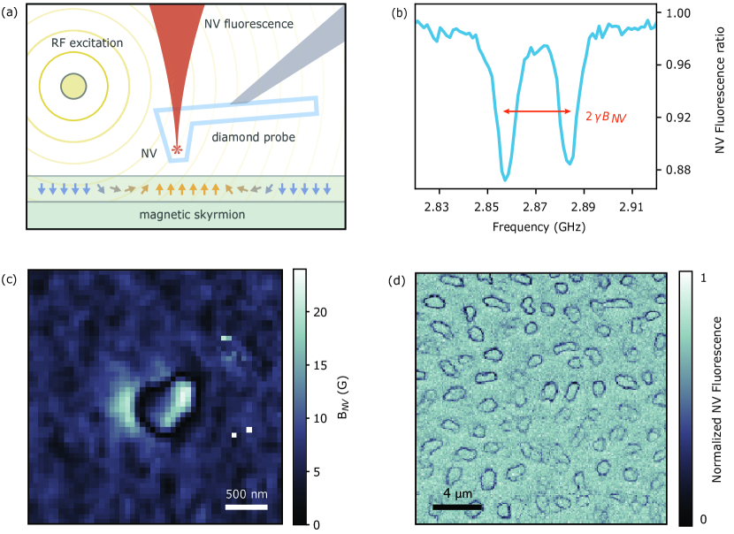
In these measurements, a single NV center in a diamond probe is scanned over the sample surface while measuring stray magnetic fields using the NV center’s optically detected magnetic resonance spectrum (Fig. 1), hence referred to as its (electron spin resonance) ESR spectrum Pelliccione et al. (2016). This spectrum is measured by sweeping the frequency of applied microwaves while monitoring the spin-state-dependent NV fluorescence rate (Fig. 1b). Magnetic fields induce a Zeeman splitting between the NV spin states that is proportional to the absolute value of the stray field along the axis of the NV— , where MHz/G is the gyromagnetic ratio of the NV. is calculated for a given ESR spectrum using this Zeeman splitting with a small correction due to fields perpendicular to the NV axis van der Sar et al. (2015). ESR measurements are used to acquire a two-dimensional map of (Fig. 1c). Based on this map, it is possible to reconstruct all vector components of the stray field Dreyer et al. (2007); Lima and Weiss (2009), and the reconstructed vector field can be used to estimate the domain wall positions comprising an individual magnetic bubble and probe the internal structure of domain walls Tetienne et al. (2015); Dovzhenko et al. (2018); Gross et al. (2016). The imaging resolution of this technique is determined by the distance from the NV to the magnetic CoFeB layer. For the image in Fig. 1c, this distance was measured to be 58 5 nm (supplementary section S2).
Measuring the ESR spectrum at each scan point is time intensive, so a faster contour imaging method is used to get information about magnetic structure. In a contour measurement, the frequency of applied microwaves is fixed while the microwave amplitude is square-wave modulated on/off at kHz frequencies. The NV fluorescence rate difference for microwaves on vs. off is measured at each point of the scan. Dark contours in the resulting image correspond to resonances of the applied microwaves with the to transitions— to first order giving contours of constant magnetic field. These contours, with a properly chosen microwave frequency, correspond to domain wall locations in the underlying thin film, as discussed below. The contour image in Fig. 1d outlines the approximate domain wall positions of a group of skyrmion bubbles.
III Magnetic phases Ta/CoFeB/MgO
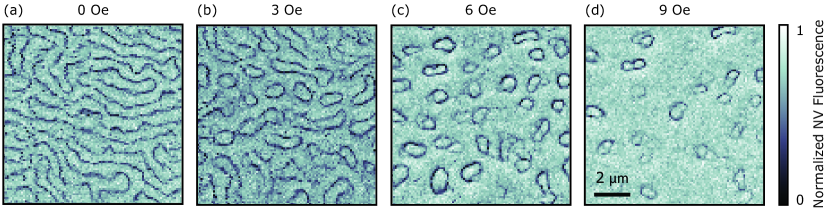
In the Ta/CoFeB/MgO thin film system, perpendicular magnetic anisotropy (PMA) due to the CoFeB/MgO interface allows for the existence of magnetic bubbles stabilized under a small magnetic field perpendicular to the film. An interfacial Dzyaloshinskii-Moriya interaction (DMI) arising from an antisymmetric exchange coupling at the interface of the ferromagnetic CoFeB and strong spin-orbit Ta layers encourages a fixed chirality of the magnetization structure of these bubbles. A wedged sub-nm Pt insertion layer between the CoFeB and MgO tunes the PMA strength by weakening Co-O and Fe-O bonds at the MgO interface. This Pt insertion layer also induces a DMI at the top CoFeB interface, modifying the total DMI strength Ma et al. (2016, 2017, 2018). A magnetic field is applied perpendicular to the sample plane giving rise to isolated skyrmions in certain regions of the PMA- phase space Yu et al. (2016). The NV fluorescence images in Fig. 2 show the evolution of the magnetic order with . At , magnetic order takes the form of stripe-like domains. As is increased, the system undergoes a first order phase transition into a skyrmion phase. In Fig. 2, a coexistence of skyrmion bubbles and stripes is seen already at 3 Oe, and several bubbles persist up to Oe. At fields larger than 10 Oe, the material transitions into a ferromagnetic phase with no magnetic features in the NV images. The images in Fig. 2 were obtained using the contour imaging method, with the frequency of the applied microwaves fixed to the NV zero-field splitting frequency of 2.870 GHz. For the small values of used, the dark contours mark the approximate domain wall positions, with a small ( 100 nm) scale offset in the direction of the NV’s in-plane projection (supplementary section S1). The width of the contour lines, which can be much smaller than the NV-sample separation, is determined by the width of the NV ESR dip and the magnetic field gradients near the domain walls Myers et al. (2014).
IV Skyrmion bubble pinning dynamics
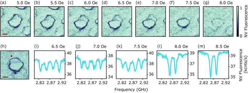
The high resolution of the NV center scanning microscope allows for the study of the microscopic structure of these bubble domains Gross et al. (2016); Dovzhenko et al. (2018). For example, contour images of domain wall position show the effects of pinning sites on skyrmion shape (Fig. 3a), which induce both a static deformation of the skyrmion as well as a dynamic instability. Figures 2c-d and the higher resolution contour images in Fig. 3a-g show irregularly shaped skyrmions, whose dramatic deviation from a disorder-free, circular shape is consistent with previously reported NV-microscopy images of a similar thin film magnetic multilayer Gross et al. (2018). The effect of pinning sites is also manifest in the evolution of skyrmion size and shape with magnetic field, as shown in Fig. 3. When is increased from 5 to 7.5 Oe the skyrmion shrinks, as seen by comparing Fig. 3a and 3f and as predicted by micromagnetic theory Thiele (1970). Interestingly, however, this process does not happen smoothly but rather discontinuously: at intermediate fields in the range of 6.0–7.5 Oe, the images in Fig. 3b-e show domain wall contours corresponding to both the larger and smaller diameter skyrmion. As the field is increased, the contrast of the larger diameter contour progressively decreases while the contrast of the smaller diameter contour increases. This behavior is explained by the domain wall hopping back and forth in time between two stable positions, progressively spending a larger fraction of its time in a smaller diameter configuration as the field is increased. Hopping that occurs on a timescale faster than the NV measurement leads to a reduction in the contrast of the contours because the NV fluorescence signal is averaged over its bright and dark states as the fluctuating field produced by the hopping domain wall brings the applied microwaves on and off resonance with the NV ESR transitions. Thus, although our measurement is too slow to detect the telegraph nature of the domain wall hopping in real time, we can detect time-averaged signatures of the dynamics through changes in contour contrast.
We can confirm the time-averaged behavior of the domain wall fluctuations by fixing the NV at a location near a fluctuating domain wall while recording the ESR spectrum, as shown in Fig. 3i-m. The position of the NV is indicated by the red dot in Fig. 3h. In the spectrum, the hopping of the domain wall appears as two dominant ESR splittings that emerge as the magnetic field is swept through the skyrmion phase. When the domain wall is near the NV, the ESR splitting is largest, given by the outer two ESR dips. The existence of other ESR dips in the spectra in Fig. 3 implies that the domain wall spends some time at another position, seen as the faint contour line cutting across the middle of the bubble in Fig. 3h. Qualitatively, the evolution of the contrast ratio between different pairs of dips in the ESR spectrum or equivalently, between domain wall branches in the contour images, gives an indication of the relative time spent in different domain wall states. As is increased, the outer pair of ESR dips grows fainter as the domain wall evolves from spending more time in the larger skyrmion diameter configuration (near the NV) to spending more time in the small diameter configuration. At 8.5 Oe, the skyrmion bubble is no longer stable and the ESR splitting is given by the NV-axis projection of .
Importantly, our NV imaging technique allows us to glean quantitative information about the time scale of the domain wall dynamics. We estimate the average hopping rate, , of the domain wall in Fig 3h to lie between 60 Hz and 14 MHz by making the following two observations. First, telegraph switching of the NV fluorescence rate was not observed on time scales slower than 16 ms, putting 60 Hz as a lower bound on . In this experiment, we could not explore faster time scales because of insufficient signal to noise ratio for measurement time bins shorter than 8 ms. An upper limit on the characteristic hopping frequency can be set by treating the domain wall position between the two pinning sites as a quasi-1D system and assuming that the dynamics is governed by an Arrhenius type thermal activation of hopping between two sites Eltschka et al. (2010), where the number of domain wall jumps in a given time is described by a Poisson process. In this case, the NV ESR spectrum is expected to take two different forms, displaying either a single resonance line or a split pair of resonance lines for each spin transition, depending on the characteristic rate of domain wall hopping and the corresponding spectral shift of the NV ESR dip. Focusing on one NV spin transition, for example , the spectral shift can be written as , where and are the NV resonance frequencies corresponding to the two domain wall positions. In the limit , distinct resonances will be observed at and , whereas in the limit , an effect similar to motional narrowing will give a spectrum with a single resonance at )/2 if, on-average, an equal amount of time is spent in both domain wall positions Bloembergen et al. (1948); Li et al. (2013). The four distinct ESR lines shown in Fig. 3b indicate that the first limit applies and that the characteristic frequency of the observed domain wall hopping is limited to MHz. This reasoning can also be applied to other observed bistable skyrmion bubble walls, for example those shown in Fig. 3c-e. Assuming that these domain wall branchings are due to a similar hopping mechanism observed in Fig. 3h-m, the fact that two domain wall positions are observed in Fig. 3c-e can be used to place a rough limit on the timescale of those domain wall dynamics as well. This novel functionality of the NV center presents an opportunity in the future to probe the dynamics more finely. Repeating spectral measurements at a different distances from the hopping bubble walls would allow one to probe frequency scales down to the NV ESR width.
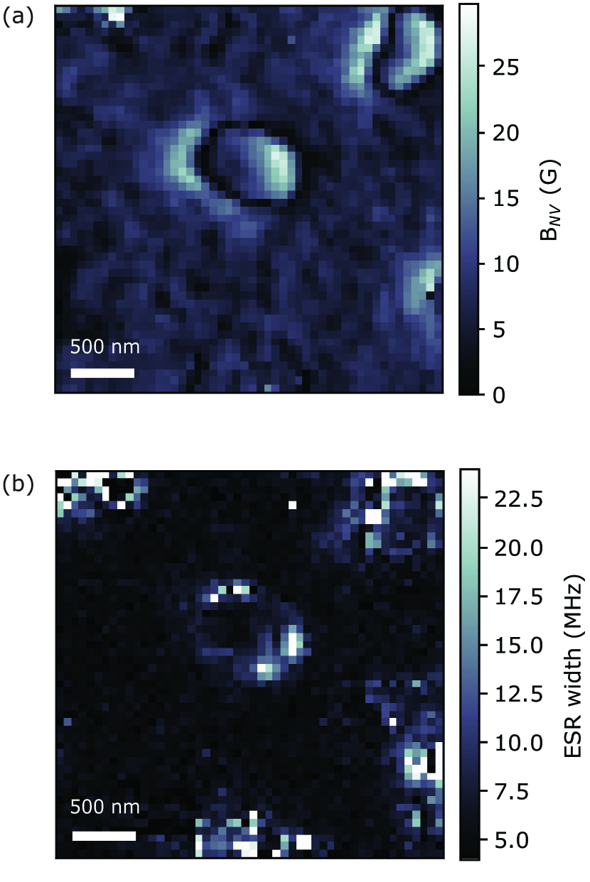
In addition to large jumps of domain wall position that produce a discrete set of ESR splittings, we also observe smaller magnetic fluctuations that broaden the NV spin transitions when the NV is positioned near a domain wall. Fig. 4b shows a spatial map of the average ESR width and comparison with a stray field image taken in the same area (Fig. 4a) clearly shows that magnetic fluctuations are enhanced near all skyrmion bubble walls, even in the absence of the clear bistabilities seen in Fig 3. We note that this broadening is not due to fluctuations in the NV-domain wall distance in regions of high magnetic fields gradient, as it is not observed near other sharp magnetic features not associated with bubble domain walls (supplementary section S3). The emergence of these enhanced fluctuations near domain walls is not well understood and can be interpreted in a few ways. It could imply the existence of small fluctuations in the position of all domain walls, driven thermally or magnetically Kronseder et al. (2015), possibly by the applied microwaves or laser light Tetienne et al. (2014). Alternatively, the spatial dependence seen in Fig. 4b could be the result of amplification or concentration of magnetic noise sources, such as spin waves, near the domain walls Mochizuki et al. (2014); Wagner et al. (2016).
V Skyrmion bubble structure
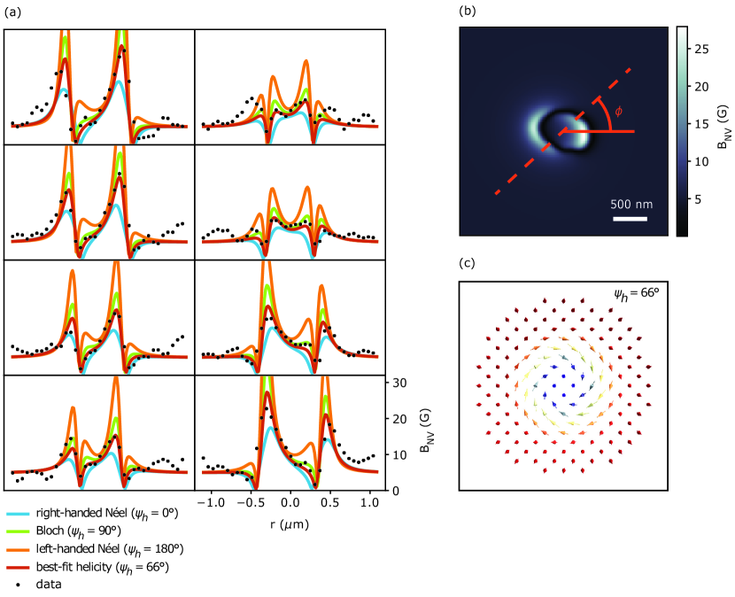
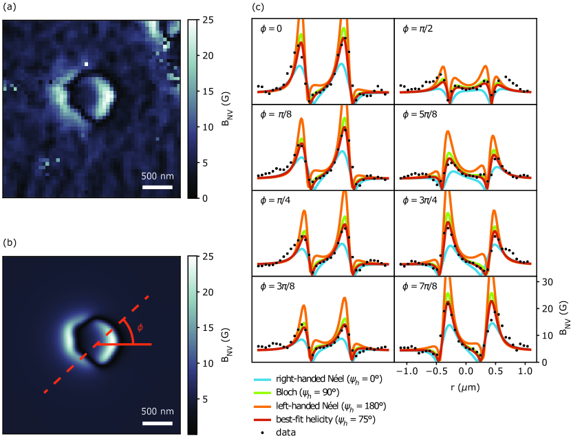
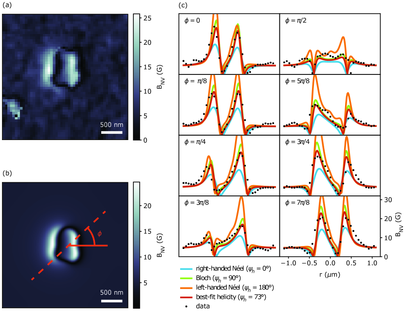
The magnetic structure of skyrmions has important implications for the viability and design of skyrmion-based devices because the structure determines important parameters of current-driven skyrmion motion, such as the skyrmion Hall angle and velocity Jiang et al. (2017); Neubauer et al. (2009); Tomasello et al. (2014); Litzius et al. (2017). However, probing the structure of skyrmion bubble is difficult due to the required nanometer-scale resolution. While many techniques can be used to determine domain wall structure in principle, there are few examples of probes that are local, non-invasive, and capable of studying a wide range of skyrmion materials. Recent NV imaging studies of magnetic thin films have established scanning NV microscopy as a useful probe of magnetic structure with all these features Dovzhenko et al. (2018); Gross et al. (2016); Tetienne et al. (2015); Hingant et al. (2015). Starting from a map of the NV-axis stray field (Fig. 4a), a quantitative reconstruction of the magnetization structure is possible but requires knowledge of several material parameters, careful calibration of the NV scan height, and some structure assumptions based on micromagnetic theory. In this work, we determine all relevant materials parameters, leaving free only the domain wall helicity angle . The helicity angle sets the rotation direction of magnetization through a cross-section of the domain wall— here defined relative to the common domain wall types as , and for right-handed Néel, Bloch, and left-handed Néel respectively. With this approach we can use the local, nanoscale nature of the NV probe to search for variations in the helicity angle along the skyrmion domain wall, which allows us to check for a fixed chirality of individual bubbles.
We start by assigning a polarity to regions of the map separated by zero-field contours. The polarity direction is determined by the direction of the applied external field. This signed field map can in turn be used to calculate the full vector components of the stray magnetic field Dovzhenko et al. (2018); Lima and Weiss (2009). The component of (where is normal to the sample) at the sample surface can be extrapolated and used to estimate the domain wall position (supplementary section S4). The magnetization pattern is then fully determined by the domain wall width , saturation magnetization , and helicity angle .
For NV-sample separations larger than , a direct measurement of is difficult and must be inferred from measurements of other parameters. Three parameters are required— , PMA energy density , and domain wall energy density . The domain wall width is given by Rohart and Thiaville (2013); Meier et al. (2017), corresponding to a magnetization profile across the domain wall . First and are measured with a SQUID magnetometer, then is directly measured with scanning NV images of the stripe phase. The domain wall energy density can be estimated from the period of the stripe spacing in these images, or calculated more directly by comparing the demagnetization energy and total domain wall length in a an image area. The exchange stiffness is then calculated from , where is the DMI energy density determined from Brillouin light scattering (BLS) measurements (supplementary section S5) Ma et al. (2016). Armed with these parameters, we can compare the expected stray field for a given helicity to that measured with the scanning NV center.
Figure 5b shows the best-fit simulated stray field corresponding to the measurement stray field in Fig. 4a. The helicity angle, is determined by a 2-dimensional fit to simulated data in 1.4 m box around the stray field features of the central skyrmion. Values obtained for other skyrmions include and (supplementary section S6). To allow for the possibility that the helicity angle can change locally along the bubble domain wall, it is instructive to compare the simulated stray field as a function of position along the domain wall. In Fig. 5a, linecuts across the measured and simulated field images are shown as a function of cut angle and helicity type. The skyrmion bubbles in this material consistently show a slightly right-handed helicity angle. A constant right-handed helicity is consistent with a non-zero winding number, but it is important to note that uncertainties in sample thickness and NV height will change the measured helicity angle. The right-handed helicity observed here agrees with BLS measurements of , but micromagnetic theory gives a smaller helicity angle for the measured (supplementary section S4).
VI Discussion and future NV studies of skyrmions
This work extends recently developed scanning NV microscopy techniques used to study multilayer skyrmion materials. Specifically, we have demonstrated that NV microscopy can simultaneously locally probe both magnetic structure and dynamics. As shown in similar thin film systems Gross et al. (2018), pinning and disorder are important factors in determining static skyrmion bubble sizes in Ta/CoFeB/MgO. We have shown that these sizes are determined dynamically, via hopping of skymion bubble domain walls between pinning sites. We have also probed the dynamics of these hopping processes and we’ve observed ubiquitous magnetic fluctuations near skyrmion bubble domain walls. Our measurements confirm the right-handed helicity of the DM interaction in this specific material structure and we have measured helicity angles in a range .
Our images highlight the importance of pinning interactions between defects and the internal degrees of freedom of skyrmion bubbles. As shown previously Woo et al. (2016), standard defect-agnostic micromagnetic models of skyrmion motion break down when material inhomogeneities exist on length scales smaller than the skyrmion size. In this work, we experimentally observe the interaction of skyrmion bubbles with these inhomogeneities. This indicates that the behavior of future devices based on the skyrmion bubbles in this material, or similar materials, will be determined by pinning interactions. Specfically, these pinning sites will likely determine the current-driven velocity and trajectory of skyrmion motion Woo et al. (2016); Litzius et al. (2017). For use in future devices, skyrmions with smaller diameters are desired Fert et al. (2017) and as the development of multilayer skyrmion material continues, the high spatial resolution of scanning NV microscopy will be increasingly important for the characterization of nanometer-scale skyrmions.
Inspired by this work, a more thorough study of the fluctuation dynamics observed here is a promising direction for future NV-based skyrmion experiments. NV noise spectroscopy has been developed as a powerful tool for obtaining information about the dynamics of noise processes in materials Agarwal et al. (2017); Myers et al. (2014, 2017); de Lange et al. (2010); van der Sar et al. (2015); Du et al. (2017). In the future, NV noise spectroscopy could be utilized to study thermal fluctuation dynamics, which are thought to play an important role in the current driven motion of skrymions Troncoso and Núñez (2014).
Acknowledgements.
We thank Preeti Ovartchaiyapong for diamond fabrication advice and Simon Meynell and Susanne Baumann for helpful discussions. The work at UCSB was supported by an Air Force Office of Scientific Research PECASE award. A portion of the work was done in the UC Santa Barbara nanofabrication facility, part of the NSF funded NNIN network. The authors acknowledge support from the Nanostructures Cleanroom Facility (NCF) at the California NanoSystems Institute (CNSI). Use of the Shared Experimental Facilities of the Materials Research Science and Engineering Center at UCSB (MRSEC NSF DMR 1720256) is gratefully acknowledged. The UCSB MRSEC is a member of the NSF-supported Materials Research Facilities Network (www.mrfn.org). Kang L. Wang acknowledges the support of NSF-1611570. Guoqiang Yu acknowledges the financial support from the National Natural Science Foundation of China [NSFC, Grants No.11874409], the National Natural Science Foundation of China (NSFC)-Science Foundation Ireland (SFI) Partnership Programme [Grant No. 51861135104], and 1000 Youth Talents Program. Xin Ma acknowledges the support from NSF grant CCF 1740352 and SRC nCORE NC-2766-A. The work at UT Austin was primarily supported as part of SHINES, an Energy Frontier Research Center funded by the U.S. Department of Energy (DOE), Office of Science, Basic Energy Science (BES) under Award No. DE-SC0012670.References
- Mühlbauer et al. (2009) S. Mühlbauer, B. Binz, F. Jonietz, C. Pfleiderer, A. Rosch, A. Neubauer, R. Georgii, and P. Böni, “Skyrmion lattice in a chiral magnet,” Science 323 (2009).
- Yu et al. (2011) X Z Yu, N Kanazawa, Y Onose, K Kimoto, W Z Zhang, S Ishiwata, Y Matsui, and Y Tokura, “Near room-temperature formation of a skyrmion crystal in thin-films of the helimagnet FeGe,” Nature Materials 10, 106–109 (2011).
- Heinze et al. (2011) Stefan Heinze, Kirsten Von Bergmann, Matthias Menzel, Jens Brede, André Kubetzka, Roland Wiesendanger, Gustav Bihlmayer, and Stefan Blügel, “Spontaneous atomic-scale magnetic skyrmion lattice in two dimensions,” Nature Physics 7, 713–718 (2011).
- Schulz et al. (2012) T Schulz, R Ritz, A Bauer, M Halder, M Wagner, C Franz, C Pfleiderer, K Everschor, M Garst, and A Rosch, “Emergent electrodynamics of skyrmions in a chiral magnet,” Nature Physics 8, 301–304 (2012).
- Jonietz et al. (2010) F. Jonietz, S. Mühlbauer, C. Pfleiderer, A. Neubauer, W. Münzer, A. Bauer, T. Adams, R. Georgii, P. Böni, R. A. Duine, K. Everschor, M. Garst, and A. Rosch, “Spin Transfer Torques in MnSi at Ultralow Current Densities,” Science 330 (2010).
- Sampaio et al. (2013) J Sampaio, V Cros, S Rohart, A Thiaville, and A Fert, “Nucleation, stability and current-induced motion of isolated magnetic skyrmions in nanostructures,” Nature Nanotechnology 8 (2013), 10.1038/NNANO.2013.210.
- Fert et al. (2013) Albert Fert, Vincent Cros, and Joao Sampaio, “Skyrmions on the track,” Nat Nano 8, 152–156 (2013).
- Yu et al. (2012) X Z Yu, N Kanazawa, WZ Zhang, T Nagai, T Hara, K Kimoto, Y Matsui, Y Onose, and Y Tokura, “Skyrmion flow near room temperature in an ultralow current density,” Nature Communications 3, 988 (2012).
- Woo et al. (2016) Seonghoon Woo, Kai Litzius, Benjamin Krüger, Mi Young Im, Lucas Caretta, Kornel Richter, Maxwell Mann, Andrea Krone, Robert M Reeve, Markus Weigand, Parnika Agrawal, Ivan Lemesh, Mohamad Assaad Mawass, Peter Fischer, Mathias Kläui, and Geoffrey S.D. Beach, “Observation of room-temperature magnetic skyrmions and their current-driven dynamics in ultrathin metallic ferromagnets,” Nature Materials 15, 501–506 (2016).
- Yu et al. (2016) Guoqiang Yu, Pramey Upadhyaya, Xiang Li, Wenyuan Li, Se Kwon Kim, Yabin Fan, Kin L. Wong, Yaroslav Tserkovnyak, Pedram Khalili Amiri, and Kang L. Wang, “Room-Temperature Creation and Spin–Orbit Torque Manipulation of Skyrmions in Thin Films with Engineered Asymmetry,” Nano Letters 16, 1981–1988 (2016).
- Moreau-Luchaire et al. (2016) C Moreau-Luchaire, C Moutafis, N Reyren, J Sampaio, C. A.F. Vaz, N. Van Horne, K Bouzehouane, K Garcia, C Deranlot, P Warnicke, P Wohlhüter, J. M. George, M Weigand, J Raabe, V Cros, and A Fert, “Additive interfacial chiral interaction in multilayers for stabilization of small individual skyrmions at room temperature,” Nature Nanotechnology 11, 444–448 (2016).
- Soumyanarayanan et al. (2017) Anjan Soumyanarayanan, M Raju, A. L.Gonzalez Oyarce, Anthony K.C. Tan, Mi Young Im, A. P. Petrovic, Pin Ho, K H Khoo, M Tran, C K Gan, F Ernult, and C Panagopoulos, “Tunable room-temperature magnetic skyrmions in Ir/Fe/Co/Pt multilayers,” Nature Materials 16, 898–904 (2017).
- Fert et al. (2017) Albert Fert, Nicolas Reyren, and Vincent Cros, “Magnetic skyrmions: Advances in physics and potential applications,” (2017).
- Jiang et al. (2017) Wanjun Jiang, Xichao Zhang, Guoqiang Yu, Wei Zhang, Xiao Wang, M. Benjamin Jungfleisch, John E Pearson, Xuemei Cheng, Olle Heinonen, Kang L Wang, Yan Zhou, Axel Hoffmann, and Suzanne G.E. Te Velthuis, “Direct observation of the skyrmion Hall effect,” Nature Physics 13, 162–169 (2017).
- Yu et al. (2010) X Z Yu, Y Onose, N Kanazawa, J H Park, J H Han, Y Matsui, N Nagaosa, and Y Tokura, “Real-space observation of a two-dimensional skyrmion crystal,” Nature 465, 901–904 (2010).
- Pollard et al. (2017) Shawn D Pollard, Joseph A Garlow, Jiawei Yu, Zhen Wang, Yimei Zhu, and Hyunsoo Yang, “Observation of stable Néel skyrmions in cobalt/palladium multilayers with Lorentz transmission electron microscopy,” Nature Communications 8 (2017), 10.1038/ncomms14761.
- Taylor et al. (2008) J. M. Taylor, P. Cappellaro, L. Childress, L. Jiang, D. Budker, P. R. Hemmer, A. Yacoby, R. Walsworth, and M. D. Lukin, “High-sensitivity diamond magnetometer with nanoscale resolution,” Nature Physics 4, 810–816 (2008).
- Degen (2008) C. L. Degen, “Scanning magnetic field microscope with a diamond single-spin sensor,” Applied Physics Letters 92, 243111 (2008).
- Balasubramanian et al. (2008) Gopalakrishnan Balasubramanian, I. Y. Chan, Roman Kolesov, Mohannad Al-Hmoud, Julia Tisler, Chang Shin, Changdong Kim, Aleksander Wojcik, Philip R. Hemmer, Anke Krueger, Tobias Hanke, Alfred Leitenstorfer, Rudolf Bratschitsch, Fedor Jelezko, and Jörg Wrachtrup, “Nanoscale imaging magnetometry with diamond spins under ambient conditions,” Nature 455, 648–651 (2008).
- Maletinsky et al. (2012) P Maletinsky, S Hong, M S Grinolds, B Hausmann, M D Lukin, R L Walsworth, M Loncar, and A Yacoby, “A robust scanning diamond sensor for nanoscale imaging with single nitrogen-vacancy centres,” Nature Nanotechnology 7, 320–324 (2012).
- Rondin et al. (2013) L Rondin, J. P. Tetienne, S Rohart, A Thiaville, T Hingant, P Spinicelli, J. F. Roch, and V Jacques, “Stray-field imaging of magnetic vortices with a single diamond spin,” Nature Communications 4 (2013), 10.1038/ncomms3279.
- Dovzhenko et al. (2018) Y. Dovzhenko, F. Casola, S. Schlotter, T. X. Zhou, F. Büttner, R. L. Walsworth, G. S. D. Beach, and A. Yacoby, “Magnetostatic twists in room-temperature skyrmions explored by nitrogen-vacancy center spin texture reconstruction,” Nature Communications 9, 2712 (2018).
- Gross et al. (2016) I. Gross, L. J. Martínez, J.-P. Tetienne, T. Hingant, J.-F. Roch, K. Garcia, R. Soucaille, J. P. Adam, J.-V. Kim, S. Rohart, A. Thiaville, J. Torrejon, M. Hayashi, and V. Jacques, “Direct measurement of interfacial Dzyaloshinskii-Moriya interaction in X—CoFeB—MgO heterostructures with a scanning NV magnetometer (X=Ta, TaN, and W),” Physical Review B 94, 064413 (2016).
- Pelliccione et al. (2016) Matthew Pelliccione, Alec Jenkins, Preeti Ovartchaiyapong, Christopher Reetz, Eve Emmanouilidou, Ni Ni, and Ania C Bleszynski Jayich, “Scanned probe imaging of nanoscale magnetism at cryogenic temperatures with a single-spin quantum sensor,” Nature Nanotechnology 11, 700–705 (2016).
- Gross et al. (2018) I. Gross, W. Akhtar, A. Hrabec, J. Sampaio, L. J. Martínez, S. Chouaieb, B. J. Shields, P. Maletinsky, A. Thiaville, S. Rohart, and V. Jacques, “Skyrmion morphology in ultrathin magnetic films,” Physical Review Materials 024406, 1–6 (2018).
- van der Sar et al. (2015) Toeno van der Sar, Francesco Casola, Ronald Walsworth, and Amir Yacoby, “Nanometre-scale probing of spin waves using single electron spins,” Nature Communications 6, 7886 (2015).
- Dreyer et al. (2007) S. Dreyer, J. Norpoth, C. Jooss, S. Sievers, U. Siegner, V. Neu, and T. H. Johansen, “Quantitative imaging of stray fields and magnetization distributions in hard magnetic element arrays,” Journal of Applied Physics 101 (2007), 10.1063/1.2717560.
- Lima and Weiss (2009) Eduardo A. Lima and Benjamin P. Weiss, “Obtaining vector magnetic field maps from single-component measurements of geological samples,” Journal of Geophysical Research: Solid Earth 114 (2009), 10.1029/2008JB006006.
- Tetienne et al. (2015) J. P. Tetienne, T Hingant, L J Martínez, S Rohart, A Thiaville, L. Herrera Diez, K Garcia, J. P. Adam, J. V. Kim, J. F. Roch, I M Miron, G Gaudin, L Vila, B Ocker, D Ravelosona, and V Jacques, “The nature of domain walls in ultrathin ferromagnets revealed by scanning nanomagnetometry,” Nature Communications 6 (2015), 10.1038/ncomms7733.
- Ma et al. (2016) Xin Ma, Guoqiang Yu, Xiang Li, Tao Wang, Di Wu, Kevin S. Olsson, Zhaodong Chu, Kyongmo An, John Q. Xiao, Kang L. Wang, and Xiaoqin Li, “Interfacial control of Dzyaloshinskii-Moriya interaction in heavy metal/ferromagnetic metal thin film heterostructures,” Physical Review B 94, 180408 (2016).
- Ma et al. (2017) Xin Ma, Guoqiang Yu, Seyed A. Razavi, Stephen S. Sasaki, Xiang Li, Kai Hao, Sarah H. Tolbert, Kang L. Wang, and Xiaoqin Li, “Dzyaloshinskii-Moriya Interaction across an Antiferromagnet-Ferromagnet Interface,” Physical Review Letters 119, 027202 (2017).
- Ma et al. (2018) Xin Ma, Guoqiang Yu, Chi Tang, Xiang Li, Congli He, Jing Shi, Kang L. Wang, and Xiaoqin Li, “Interfacial Dzyaloshinskii-Moriya Interaction: Effect of 5d Band Filling and Correlation with Spin Mixing Conductance,” Physical Review Letters 120, 157204 (2018).
- Myers et al. (2014) B A Myers, A Das, M C Dartiailh, K Ohno, D D Awschalom, and A C Bleszynski Jayich, “Probing surface noise with depth-calibrated spins in diamond,” Physical Review Letters 113 (2014), 10.1103/PhysRevLett.113.027602.
- Thiele (1970) A. A. Thiele, “Theory of the static stability of cylindrical domains in uniaxial platelets,” Journal of Applied Physics 41, 1139–1145 (1970).
- Eltschka et al. (2010) M. Eltschka, M. Wötzel, J. Rhensius, S. Krzyk, U. Nowak, M. Kläui, T. Kasama, R. E. Dunin-Borkowski, L. J. Heyderman, H. J. van Driel, and R. A. Duine, “Nonadiabatic Spin Torque Investigated Using Thermally Activated Magnetic Domain Wall Dynamics,” Physical Review Letters 105, 056601 (2010).
- Bloembergen et al. (1948) N. Bloembergen, E. M. Purcell, and R. V. Pound, “Relaxation Effects in Nuclear Magnetic Resonance Absorption,” Physical Review 73, 679–712 (1948).
- Li et al. (2013) Jian Li, M. P. Silveri, K. S. Kumar, J. M. Pirkkalainen, A. Vepsäläinen, W. C. Chien, J. Tuorila, M. A. Sillanpää, P. J. Hakonen, E. V. Thuneberg, and G. S. Paraoanu, “Motional averaging in a superconducting qubit,” Nature Communications 4, 1420 (2013).
- Kronseder et al. (2015) M. Kronseder, T. N.G. Meier, M. Zimmermann, M. Buchner, M. Vogel, and C. H. Back, “Real-time observation of domain fluctuations in a two-dimensional magnetic model system,” Nature Communications 6, 6832 (2015).
- Tetienne et al. (2014) J. P. Tetienne, T Hingant, J. V. Kim, L. Herrera Diez, J. P. Adam, K Garcia, J. F. Roch, S Rohart, A Thiaville, D Ravelosona, and V Jacques, “Nanoscale imaging and control of domain-wall hopping with a nitrogen-vacancy center microscope,” Science 344, 1366–1369 (2014).
- Mochizuki et al. (2014) M. Mochizuki, X. Z. Yu, S. Seki, N. Kanazawa, W. Koshibae, J. Zang, M. Mostovoy, Y. Tokura, and N. Nagaosa, “Thermally driven ratchet motion of a skyrmion microcrystal and topological magnon Hall effect,” Nature Materials 13, 241–246 (2014).
- Wagner et al. (2016) K Wagner, A Kákay, K. Schultheiss, A Henschke, T Sebastian, and H Schultheiss, “Magnetic domain walls as reconfigurable spin-wave nanochannels,” Nature Nanotechnology 11, 432–436 (2016).
- Neubauer et al. (2009) A Neubauer, C Pfleiderer, B Binz, A Rosch, R Ritz, P G Niklowitz, and P Böni, “Topological Hall effect in the A-phase of MnSi,” Physical Review Letters 102, 186602 (2009).
- Tomasello et al. (2014) R. Tomasello, E. Martinez, R. Zivieri, L. Torres, M. Carpentieri, and G. Finocchio, “A strategy for the design of skyrmion racetrack memories,” Scientific Reports 4, 6784 (2014).
- Litzius et al. (2017) Kai Litzius, Ivan Lemesh, Benjamin Krüger, Pedram Bassirian, Lucas Caretta, Kornel Richter, Felix Büttner, Koji Sato, Oleg A. Tretiakov, Johannes Förster, Robert M. Reeve, Markus Weigand, Iuliia Bykova, Hermann Stoll, Gisela Schütz, Geoffrey S.D. Beach, and Mathias Klaüi, “Skyrmion Hall effect revealed by direct time-resolved X-ray microscopy,” Nature Physics 13, 170–175 (2017).
- Hingant et al. (2015) T. Hingant, J. P. Tetienne, L. J. Martínez, K. Garcia, D. Ravelosona, J. F. Roch, and V. Jacques, “Measuring the magnetic moment density in patterned ultrathin ferromagnets with submicrometer resolution,” Physical Review Applied 4, 014003 (2015).
- Rohart and Thiaville (2013) S. Rohart and A. Thiaville, “Skyrmion confinement in ultrathin film nanostructures in the presence of Dzyaloshinskii-Moriya interaction,” Physical Review B 88, 184422 (2013).
- Meier et al. (2017) T. N.G. Meier, M Kronseder, and C H Back, “Domain-width model for perpendicularly magnetized systems with Dzyaloshinskii-Moriya interaction,” Physical Review B 96 (2017), 10.1103/PhysRevB.96.144408.
- Agarwal et al. (2017) Kartiek Agarwal, Richard Schmidt, Bertrand Halperin, Vadim Oganesyan, Gergely Zaránd, Mikhail D. Lukin, and Eugene Demler, “Magnetic noise spectroscopy as a probe of local electronic correlations in two-dimensional systems,” Physical Review B 95, 155107 (2017).
- Myers et al. (2017) B A Myers, A Ariyaratne, and A. C.Bleszynski Jayich, “Double-Quantum Spin-Relaxation Limits to Coherence of Near-Surface Nitrogen-Vacancy Centers,” Physical Review Letters 118 (2017), 10.1103/PhysRevLett.118.197201.
- de Lange et al. (2010) G. de Lange, Z. H. Wang, D. Ristè, V. V. Dobrovitski, and R. Hanson, “Universal dynamical decoupling of single solid spin from spin bath,” Science 330 (2010).
- Du et al. (2017) Chunhui Du, Toeno van der Sar, Tony X Zhou, Pramey Upadhyaya, Francesco Casola, Huiliang Zhang, Mehmet C Onbasli, Caroline A Ross, Ronald L Walsworth, Yaroslav Tserkovnyak, and Amir Yacoby, “Control and local measurement of the spin chemical potential in a magnetic insulator,” Science 357, 195–198 (2017).
- Troncoso and Núñez (2014) Roberto E. Troncoso and Alvaro S. Núñez, “Thermally assisted current-driven skyrmion motion,” Physical Review B - Condensed Matter and Materials Physics 89, 224403 (2014).
- Johnson et al. (1996) M T. Johnson, P J H. Bloemen, F J A. den Broeder, and J J. de Vries, “Magnetic anisotropy in metallic multilayers,” Rep. Prog. Phys 59, 1409–1458 (1996).
- Jang et al. (2010) Soo Young Jang, S. H. Lim, and S. R. Lee, “Magnetic dead layer in amorphous CoFeB layers with various top and bottom structures,” Journal of Applied Physics 107, 09C707 (2010).
- Sinha et al. (2013) Jaivardhan Sinha, Masamitsu Hayashi, Andrew J. Kellock, Shunsuke Fukami, Michihiko Yamanouchi, Hideo Sato, Shoji Ikeda, Seiji Mitani, See Hun Yang, Stuart S. P. Parkin, and Hideo Ohno, “Enhanced interface perpendicular magnetic anisotropy in Ta—CoFeB—MgO using nitrogen doped Ta underlayers,” Applied Physics Letters 102, 242405 (2013).
- Buford et al. (2016) Benjamin Buford, Pallavi Dhagat, and Albrecht Jander, “Estimating exchange stiffness of thin films with perpendicular anisotropy using magnetic domain images,” IEEE Magnetics Letters 7, 1–5 (2016).
- Donahue and Porter (1999) M J. Donahue and D G. Porter, OOMMF User’s Guide, Version 1.0, Tech. Rep. (NIST, 1999).
- Saratz (2010) Niculin Andri Saratz, Inverse Symmetry Breaking in Low-Dimensional Systems, Ph.D. thesis (2010).
- Thiaville et al. (2012) André Thiaville, Stanislas Rohart, Emilie Jué, Vincent Cros, and Albert Fert, “Dynamics of Dzyaloshinskii domain walls in ultrathin magnetic films,” EPL 100, 57002–p1–p6 (2012).
Supplementary Information: Single spin sensing of domain wall structure and dynamics in a thin film skyrmion host
S1. Contour imaging— domain wall position
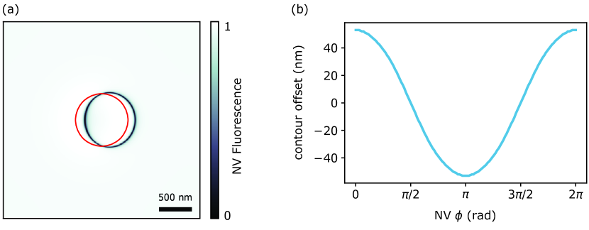
The NV contour imaging method consists of fixing an applied microwave frequency while monitoring the NV fluorescence or the ratio of NV fluorescence for microwaves on vs. off. Dark contours in a contour scanning NV image correspond to locations where the stray field from the sample cause NV spin transitions to line-up with the applied microwave frequency. As stated in the main text, at low external fields and with magnetic domain wall widths much smaller than the bubble or stripe domains, 2.870 GHz contour images give good approximations to the domain wall positions. Figure S1a shows a simulated zero-field contour from a circular domain wall with a 9.5 Oe external magnetic field. The zero-field contour is shifted slightly along the direction of the NV center’s in-plane projection. Figure S1b shows the offset (in nm) between the position of a straight Bloch domain wall and its zero-field contour in the imaging plane as a function of the in-plane NV angle relative to a direction normal to the domain wall ().
S2. NV height calibration
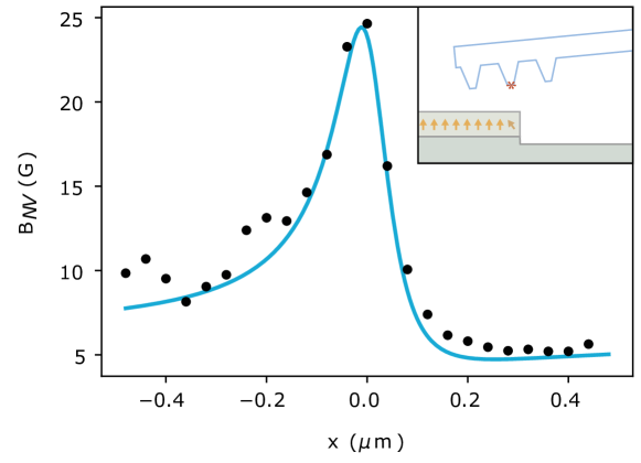
The NV scan height above the magnetic CoFeB layer determines the spatial resolution of the NV imaging technique and this height an important parameter in reconstructing the magnetization. The NV height is calibrated by scanning the NV across a step edge that has been etched through the magnetic layer Tetienne et al. (2015); Hingant et al. (2015). The step edge is defined with electron beam lithography and the thin-film stack is etched with Ar ion milling. An external magnetic field is applied to saturate the film and the stray field is measured as a function of position from the step edge. Assuming a sharp step edge, with a magnetic layer thickness much less than the NV height , the stray field profile is given by
| (1) | ||||
| (2) |
where is the external magnetic field and the step edge runs along the line .
In the presence of non-zero DMI, the magnetization rotates at the step edge Tetienne et al. (2015). This rotation angle at the edge is given by Rohart and Thiaville (2013)
| (3) |
and is described by
| (4) |
which for small values of gives,
| (5) | ||||
| (6) | ||||
| (7) |
Taking this rotation into account, the stray field can be calculated as
| (8) | ||||
| (9) |
For the low DMI Ta/CoFeB structure studied here, this magnetization rotation at the step edge gives only a few nm correction to the NV height calibration. The NV height above the CoFeB layer is extracted by fitting the stray field given by these expressions to the measured field along the NV axis. The magnetic moment density is measured separately with SQUID (see Sec. S2). An example of one of the calibration curves is shown in Fig. S2. Twenty of these linecuts were taken at different points along a 2 m length of the step edge. The NV height and height error used in magnetization reconstruction calculations is given by the mean and standard deviation of these fits respectively.
The angles of the NV axis with respect to the edge and sample normal are calibrated separately using an external magnetic field. The NV height calibration depends critically on the profile of the magnetization at the etched edge. Any redeposition of magnetic material or damage to the magnetic structure at the edge induced by ion milling will lead to systematic errors in the NV height.
S3. ESR widths at etched step edge
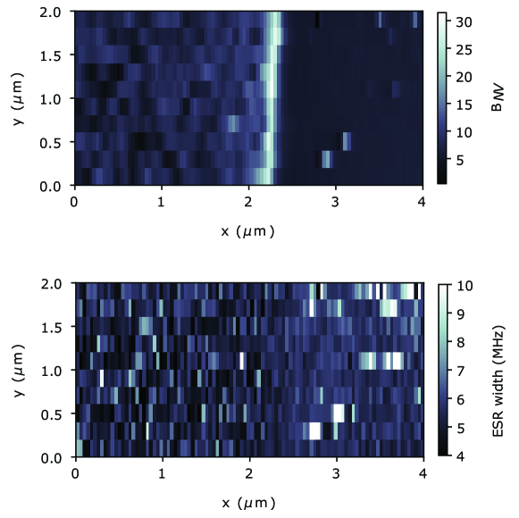
To verify that the ESR broadening observed near domain walls (Fig. 4 from the main text) results from magnetic noise intrinsic to the domain wall and is not, for example, due to tip oscillation in a high field gradient, the NV ESR width is measured as the NV is scanned across a step edge etched in the magnetic thin film. Figure S3 plots the stray magnetic field and the ESR width in the same imaging area. The large gradient above the step edge (Fig. S3 top, bright vertical line) does not have an associated increase in ESR width (Fig. S3 bottom), thus confirming that NV motion in a high field gradient is not responsible for the ESR broadening observed near skyrmion domain walls in Fig 4 of the main text.
S4. Extracting material parameters
A quantitative comparison of a skrymion’s stray field to its underlying magnetic structure necessitates knowledge of several material parameters, as pointed out in the discussion of Fig. 5 in the main text. Specifically we require a knowledge of , , and domain wall width , and we assume an analytic form (see section S5) for the domain wall profile. The domain wall position is also needed and is given by the NV images. To estimate , which cannot be measured directly with our NV center for lack of spatial resolution, we combine bulk measurements of the effective magnetic anisotropy energy density and the magnetic surface density with NV measurements of the domain wall energy density .
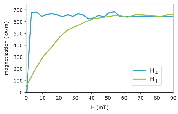
The parameters and are calculated from hysteresis curves obtained with a Quantum Design MPMS 5XL SQUID. The magnetic moment is measured as a function of an applied field both parallel and normal to the film plane (Fig. S4). After dividing the measurement magnetic moment by the thin film volume, is the saturation value, while is given by the area between the parallel and normal curves Johnson et al. (1996). These measurements give A, where the uncertainty is given the standard deviation of the saturated SQUID value. This gives A/m and J/m3 for a film thickness nm. Calculating the uncertainty in and is trickier because their values depend on the film thickness . The value of used in these calculations is given by the measured deposition thickness, but we note that magnetic dead layers have been observed in CoFeB films at Ta or MgO interfaces Jang et al. (2010); Sinha et al. (2013). A non-zero dead layer thickness would lead to different values of and and differences in the magnetization reconstruction.
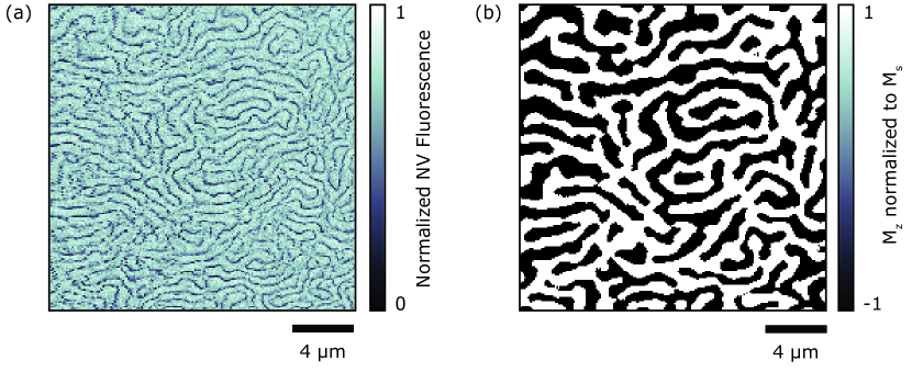
Armed with values of and , it is possible to measure the domain wall energy density from stripe-phase NV images. The NV scan can be used to calculate the demagnetization energy and total domain wall length in the image area. The domain wall energy density is then calculated based on an energy minimization that balances variation in the demagnetization energy and domain wall length measured for a particular imaging area Buford et al. (2016). Starting from a zero-field stripe image, a polarity () is assigned to the two image regions (Fig. S5). The demagnetization energy in the imaged area is calculated with OOMMF Donahue and Porter (1999) using mirror symmetric boundaries. The total length of the domain walls in this image is also measured and both values are normalized by the image area giving and . The domain wall energy density can then be obtained as in Buford et al. (2016) by calculating the variation of and with respect to the characteristic stripe periodicity ,
| (10) |
These variations can be related to variations in the imaging resolution,
| (11) |
| (12) |
This procedure gives mJ/m2. The domain wall energy density can be used in turn to calculate and
| (13) | |||
| (14) |
The DMI strength measured via Brillioun light scattering (BLS) is found to be J/m2, giving an exchange stiffness pJ/m and domain wall width nm. The extracted value of is in good agreement with the value measured with BLS (section S5). This method of estimating can be checked against an analytic form for parallel stripe domains Saratz (2010)
| (15) |
Identifying characteristic image length scale in the image Fourier decomposition, nm. This gives a domain wall width nm.
However, a non-zero dead layer thickness will alter either calibration of domain wall width. For example, assuming a dead layer thickness of 0.36 nm, similar to Jang et al. (2010), the same analysis gives the parameters A/m, J/m3, pJ/m, and nm.
S5. BLS measurements of material parameters
Spin wave dispersion in BLS measurements:
The spin waves probed here are Damon-Eshback (DE) modes with propagation directions perpendicular to external magnetic field. The spin wave dispersion is described by Ma et al. (2017):
| (16) | ||||
where is the magnitude of the external magnetic field, is the gyromagnetic ratio, is the exchange stiffness constant, with the CoFeB thickness, is the interfacial magnetic anisotropy which mainly originates from the CoFeB/MgO interface, describes a correction in frequency due to the non-reciprocity of the DE spin waves, and is the DMI coefficient.
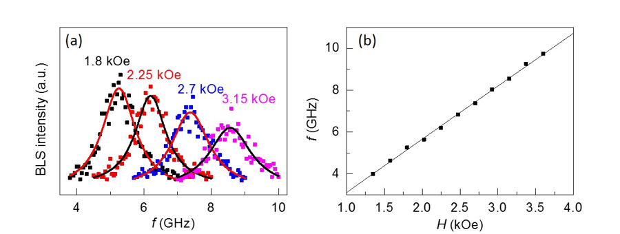
Field-dependent BLS measurements to determine magnetic anisotropy:
Magnetic field dependent BLS measurements were performed to determine the magnetic anisotropies. In order to improve the accuracy of magnetic anisotropy measurements, we performed BLS measurements with normal incidence of light (). As a result, Eq. 16 is simplified to with . Figure S6(a) shows that the BLS spectra under different for the Ta/CoFeB/Pt/MgO sample. The BLS spectra can be well fitted with Lorentzian functions, and the resonance frequency increases with . Figure S6(b) displays as a function of , which can be well fitted by the simplified Eq. 16 at with kOe (solid lines). The negative sign of indicates that the easy axis of magnetization is perpendicular to the thin film plane.
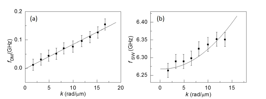
k-dependent BLS measurements to determine DMI coefficient and exchange stiffness :
Both the DMI coefficient and exchange stiffness constant can also be determined from the momentum-resolved BLS measurements. We determine the by subtracting the and in Eq. 16:
| (17) |
Figure S7 shows that the linear correlation between and , where the slope is used to determine J/m2. The positive sign of indicates that the right-handed magnetic chirality is preferred in the material system. The exchange stiffness is determined by averaging and in Eq. 16:
| (18) | ||||
Figure S7(b) plots the as a function of , where increases with larger and can be well fitted with the above simplified equation. As a result, we derived the exchange stiffness pJ/m.
S6. Reconstructing helicity angle
Constructing the underlying magnetization pattern from a stray field measurement is not trivial. The mapping from magnetization to stray field is not one-to-one and cannot be inverted. In order to say anything about the magnetization pattern given the measured stray field, we must measure several materials parameters (section S4) and make further assumptions based on micromagnetic theory. Recent studies dealing with these issues have taken two main approaches: assume a domain wall profile based on micromagnetic theory Tetienne et al. (2015); Gross et al. (2016), or fix a local magnetization gauge or helicity angle Dovzhenko et al. (2018). The first method has the advantage that the local helicity angle can be extracted and need not be assumed as fixed along the entire length of a domain wall, but the second method has the nice property that it does not rely on an analytic form of the domain wall profile (DMI will lead to deviations in domain wall shape Thiaville et al. (2012)). In this work we use the reconstruction methods described in Dovzhenko et al. (2018) to estimate the domain wall position in the Bloch magnetization gauge (), but then fix the magnetization pattern using the analytic form of a thin film domain wall to calculate the stray magnetic field as a function of helicity angle.
For the low external fields used in these measurements, the stray field along the NV axis changes sign at different points in the imaging plane. Since the NV measures only the absolute value of the stray field, estimation of the domain wall position requires us to assign a polarity to regions of the image separated by zero-field contours. Reconstruction of the full vector magnetic field can then proceed as described in Dovzhenko et al. (2018); Lima and Weiss (2009). The component of magnetization is easily calculated in the Bloch gauge by projecting Fourier components of the stray field down to the sample surface using a stray field transfer function , similar to Dreyer et al. (2007),
| (19) | |||
| (20) |
In our case, this procedure leads to amplification of image noise because of the somewhat large NV scan height. is then used to find the position of the domain wall, but is not used to simulate the stray field. The magnetization components calculated relative to the domain wall position are
| (21) | |||
| (22) | |||
| (23) |
| (24) |
where . Using the BLS value of , the expected helicity angle is . However, assuming a fixed helicity angle, the best fit helicity angles given by the images in Figure 4, S8, and S9 are 66∘, 75∘, and 73∘ respectively. These best fit helicity values depend on the extracted material parameters described in section S4, and as such, the main source of uncertainty in determining these values is due to a possible systematic error caused by an unknown magnetic dead layer thickness. Using the the material parameters extracted for the case of the 0.36 nm thick magnetic dead layer described in section S4, the best fit helicity values for the skyrmion bubbles in Figure 4, S8, and S9 are 80∘, 86∘, and 85∘ respectively.