Engineering Nonlinear Response of Superconducting Niobium Microstrip Resonators via Aluminum Cladding
Abstract
In this work, we find that Al cladding on Nb microstrip resonators is an efficient way to suppress nonlinear responses induced by local Joule heating, resulting in improved microwave power handling capability. This improvement is likely due to the proximity effect between the Al and the Nb layers. The proximity effect is found to be controllable by tuning the thickness of the Al layer. We show that improving the film quality is also helpful as it enhances the microwave critical current density, but it cannot eliminate the local heating.
I Introduction
Recently, superconducting planar resonators zmuidzinas have found applications in magnetic resonance because their low dissipation and small mode volume have greatly improved the sensitivity of spin detection xiang ; kurizki ; benningshof2013 ; malissa2013 ; sigillito2014 ; grezes2014 ; bienfait2016a ; eichler2017 ; sigillito2017 ; probst2017 . In addition to the detection sensitivity, superconducting resonators are required to handle strong microwave pulses for efficient spin manipulation. However, microwave power handling capability of superconducting planar resonators has been an issue—if we apply a strong microwave pulse, the nonlinearity of the resonator participates such that the actual microwave magnetic field that a spin sees becomes significantly different from what we intended.
Regarding the Duffing-type nonlinearity duffing , it is known that we can design a pulse which can compensate the nonlinear response as the Duffing-type nonlinearity can be easily modeled and controlled using nonlinear circuit models oates1993 ; tholen2009 ; ku2010 ; swenson2013 ; mohebbi2014 ; hincks2015 . However, many reported nonlinear responses of type-II superconducting resonators are very difficult to model, thus not controllable: the shape of S-parameter curves becomes irregular and greatly suppressed even at modest microwave power. This type of nonlinearity has been attributed to local Joule heating, often called a hot spotgurevich1987 , followed by switching of weak links to the normal state jacobs1996 ; wosik1997 ; wosik1999 ; purnell2004 ; abdo2006 ; wosik2009 ; ghigo2009 ; ghigo2010 ; ku2010 ; brenner2011 ; kurter2011 . Thus, it is crucial to minimize this undesired nonlinear response for magnetic resonance applications.
In this work, we investigated ways to suppress the nonlinearity due to local Joule heating by improving the film quality (Sec. III) and Al cladding (Sec. IV) tang2017 . We first showed that local Joule heating is the dominant source of the nonlinearity of pure Nb microstrip resonators. Then, we found that a resonator made of better quality film showed a significantly higher microwave critical current, but the major mechanism of the nonlinearity remains the same. Meanwhile, Al cladding effectively eliminated the nonlinear responses induced by local Joule heating. This improved microwave power handling capability is likely due to the proximity effect between the Al and the Nb layers deGennes ; jin ; vissers2013 ; oxford1 . The existence of the proximity effect was confirmed experimentally by studying how magnetic field dependence of the resonance frequency and the quality factor change as we tune the thickness of the Al layer (Sec. V). This study also showed that the proximity effect is controllable by tuning the thickness of the Al layer.
II Methods
| Res. | Composition | (GHz) | ||
|---|---|---|---|---|
| Al-0L | Nb 50 | low | 10.0728 | 14300 |
| Al-5L | Al 5/Nb 50/Al 5 | low | 9.9764 | 21000 |
| Al-10L | Al 10/Nb 50/Al 10 | low | 10.0672 | 23600 |
| Al-0H | Nb 50 | high | 10.0792 | 27500 |
| Res. |
|
|
|
|
|
|
|
|
||||||||||||||||
|---|---|---|---|---|---|---|---|---|---|---|---|---|---|---|---|---|---|---|---|---|---|---|---|---|
| Al-0L | 10 | 0.6 | RT | RT | Yes | 7.2 | 17 | |||||||||||||||||
| Al-0H | 10-10 | 1.7 | 550 | 770 | No | 9.3 | 2.9 |
Four microstrip resonators with different film quality and Al cladding thickness were used. Two of them were pure Nb resonators with different film quality. The film quality was controlled mainly by the temperature of the substrate at the time of the film growth; the higher substrate temperature resulted in higher critical temperature and lower residual resistivity, i.e., a better quality film. The other two resonators were trilayer resonators—Nb resonators with Al cladding. For all resonators, the ground plane was made of a pure Nb layer, and the thickness of Nb layers, including the ground plane, was 50 nm. Since our resonators are all microstrip resonators, i.e., double-sided film, there is no complication for making the ground plane and the microstrip with different material compositions.
The resonators are labeled with the thickness of the Al layers and the substrate temperature as shown in Table 1; Al-5L and Al-10L indicate that the thickness of each layer is Al/Nb/Al = 5/50/5 nm and 10/50/10 nm, respectively, and the films were grown at low temperature. A control sample of pure Nb grown at higher temperature is labeled Al-0H. The detailed growth conditions of the Nb films are summarized in Table 2. The trilayer resonators were grown in one vacuum cycle with the same condition as that of Al-0L to avoid potential alloying at elevated temperature. High-resolution XRD pattern of the trilayer film can be found in Ref. tang2017, . All films were grown by DC magnetron sputtering on both sides of -plane sapphire wafers (double-side-polished 430 m thick and 2 inch diameter). Then the resonators were fabricated by optical lithography and dry etching.
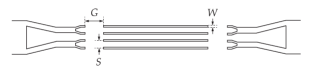
The resonators are straight half-wavelength resonators; each resonator was composed of four microstrips as shown in Fig. 1 (Ref. mohebbi2014, ). The geometry of all resonators are identical, except the coupling gap ( in Fig. 1). For Al-0H, the coupling gap was 400 m; for other resonators, the coupling gap was 350 m. The resonance frequencies of all resonators below 20 mK without a magnetic field are about 10 GHz.
The reason for employing microstrip resonators is that this geometry can generate uniform microwave fields above the strips compared to coplanar resonators.benningshof2013 Therefore, we believe a microstrip geometry is more suitable for electron spin resonance (ESR) of thin films, which is our research interest.mohebbi2014 ; kwon As a trade-off, the less confined field profile inherently leads to more radiation loss and dielectric loss; thus, our resonators show lower internal quality factor (see Table 4) values than corresponding coplanar resonators.
The measurements were made in a cryogen-free dilution refrigerator (Leiden CF250). The resonator is aligned with a magnetic field using a goniometer (Attocube ANGt101) with the precision mdeg at 0.1 K. For more details, see Sec. III of Ref. kwon, .
Full S-parameters were collected using a vector network analyzer (VNA, Agilent N5230A). The resonance frequency and the loaded quality factor were obtained by fitting the magnitude of the measured to a complex Lorentzian function kwon . The external quality factor was obtained using the formula , where IL is the insertion loss in dB (Ref. sage2011, ). The internal quality factor was obtained from the relation . The input microwave power was estimated by (in dB), where is the setting power of the VNA, and CL is the loss in cables from the VNA to the input capacitor of the resonator.111The estimated insertion loss can vary 1–2 dB from one package to the next mainly due to imperfect package assembling. Such a deviation is not crucial for the power dependence, but it may change the values of the internal quality factor in Table 4 about 20–30%. The circulating power was estimated using . The maximum value of the microwave current circulating in the resonator was estimated using (Ref. oates1990, ), where is the characteristic impedance of the resonator, which is designed to be about 50 .
III Improving the Film Quality
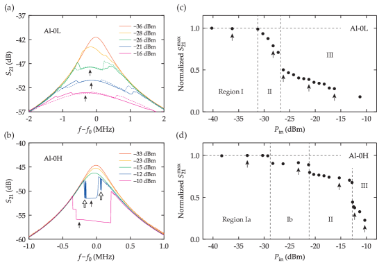
Figure 2(a) shows curves of Al-0L at various . As increases, the resonance peak becomes rapidly suppressed and irregular. To know the source of this nonlinearity, we plotted the maximum value of () as a function of [Fig. 2(c)]. Note that the plot can be divided into three regions based on the shape of the curve: In the low-power region (region I), the curve is Lorentzian. As increases (region II), the curve becomes asymmetric and distorted. Finally, the resonator enters region III with the onset of jump in . In this region, the shape of the curve is very irregular; when the curves were swept in the opposite direction, the curve becomes reflected shape [dashed lines in Fig. 2(a)].
The same measurements were done with a resonator made of a better quality Nb film, Al-0H [Fig. 2(b)]. There are several notable differences between Al-0L and Al-0H: First, for Al-0H, the shape of the curve is Lorentzian and the resonance frequency remains the same until reaches dBm. However, there is an abrupt drop in and the quality factor near dBm; hence, we divide region I into regions Ia and Ib. The reason for this sudden drop is unclear at this stage.
Secondly, in region III, Al-0H shows cratered Lorentzian shapes and bistability, which have been accounted for switching of weak links, such as grain boundaries, to the normal state wosik1997 ; wosik1999 ; purnell2004 ; abdo2006 ; wosik2009 ; ghigo2009 ; ghigo2010 ; ku2010 ; brenner2011 ; kurter2011 ; gurevich1987 ; hylton1988 ; hylton1989 ; halbritter1990 ; halbritter1992 ; halbritter1995 . For Al-0L, the irregular shape is reproducible from sweep to sweep—there is no notable bistable behavior. This suggests that the spread in the microwave critical currents of Al-0L more significant than that of Al-0H such that bistable behaviors are averaged out, resulting in spike-like features (see Fig. 9 in Ref. ghigo2010, ).
| Res. | |||||
|---|---|---|---|---|---|
| Al-0L | 1.2 | 4 | |||
| Al-0H | 11 | 18 |
For quantitative understanding, we estimated microwave current densities at the boundaries between regions; the values are summarized in Table 3.222To obtain , we needed factors of the data in region II. Since the shape of curves is slightly asymmetric, the Lorentzian fitting was not perfect. We just used the values from the fitting because the asymmetry was not significant. We also tried a 3 dB bandwidth and it gave similar values. Here, note that, , which can be considered as the microwave critical current density, is about one order of magnitude less than for both resonators, suggesting that the microwave power handling capability is not limited by intrinsic and global properties of superconductivity. This supports that the dominant mechanism for the nonlinearity of pure Nb films is local Joule heating. Also note that of the resonator made of a better quality film (Al-0H) are about one order of magnitude higher than that of the resonator with low film quality (Al-0L). This shows that improving the film quality enhances the microwave critical current density, but it does not change the dominant mechanism for the nonlinearity.
IV Aluminum Cladding
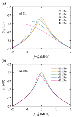
Figure 3 shows curves at various after Al cladding. Note that Al cladding changes the nonlinear response dramatically: Al-5L and Al-10L show the Duffing-type nonlinearity instead of irregular shapes. Since this type of nonlinearity is controllable using nonlinear circuit models oates1993 ; ku2010 ; swenson2013 ; mohebbi2014 ; hincks2015 , as mentioned in Sec. I, we can say that Al cladding improves the high-power handling capability.
The qualitative change in the nonlinearity after Al cladding is likely due to current bypasses provided by Al near weak links in the Nb layer. The superconductivity of these Al bypasses is strengthened by the proximity effect such that the critical current density and the critical field of the Al layers are substantially enhanced. Here, to provide reliable bypasses, the Al layers need to cover the surface of the Nb layers perfectly. In this regard, Al and Nb combination is special because Al grown at room temperature wets on the surface of Nb ideallychang1987 . The reason for this is that the bonding between Al and Nb is stronger than that between Al and Al.
Other possible roles of Al cladding, such as protection against oxidation of the Nb layer halbritter1987 ; halbritter1988 and enhancing the thermal conductivity feshchenko2017 , can reduce the number of weak links and local Joule heating; however, they cannot fully account for such a qualitative change. Here, note that a normal metal layer can do the same things, except strengthening the superconductivity. In Refs. ghigo2009, ; ghigo2010, , a 35 nm thick layer of Au was deposited on an MgB2 thin film, but the nonlinear behavior due to switching of weak links remained largely unchanged. In addition, another way to reducing the number of weak links, improving the film quality, does not change the dominant mechanism for the nonlinearity as shown in Sec. III. From these results, we believe that the qualitative change in nonlinear response after Al cladding is mainly due to the proximity effect.
Even after the switching of weak links are eliminated, further Al cladding can still assist, as shown in Fig. 3(b). Note that, in Table 4, Al-10L shows higher internal quality factor (), which implies that Al cladding reduces the surface resistance, and lower effective residual resistivity () compared to Al-5L. (See Sec. V for further explanation regarding Table 4.) These results suggest that the observed nonlinearity of the trilayer resonators is driven by global heatingwosik1999 ; wosik2009 which is generated through the following process: When the circulating power is low enough such that there is no notable nonlinear response, the heat balance between the cooling power and the dissipated power due to the finite surface resistance is fulfilled. At this stage, there are not many thermally-excited quasiparticles because of the low temperature (0.2 K). When the circulating power passes a certain level, at which the dissipated power is greater than the cooling power, quasiparticles are excited and participate in the power dissipation, which is proportional to , where is the residual resistivity kwon .
The intrinsic GL nonlinearitygittleman1965 ; lam1992 ; clem2012 does not account for the nonlinearity of the trilayer resonators because the GL nonlinearity is known to be much more reactive than shown by the data in Fig. 3 (Ref. golosovsky1995, ). Indeed the data in Fig. 4 of Sec. V, which follow the GL equations closely, the shift of about 1 MHz does not result in notable change in and . In addition, vortex penetration into grains is also unlikely because, if vortices were created by a microwave current and penetrated into the grains, a hysteretic behavior would be observed due to vortex pinning; in other words, the curve would not go back to its original position and shape once high was applied ghigo2009 . Such behavior was not observed at zero field for all resonators.
In a modest field parallel to the microwave current , we find that the results in Figs. 2 and 3 are largely unchanged. Some of the representative data are shown in Fig. S3. In a field perpendicular to the film , we found that applying a high microwave current results in magnetic hysteresis caused by suppression of the edge barrier and consequent injection of vortices. Here, these vortices are created by , not by the microwave current. The supporting data and analysis are in Sec. S3.
V The Proximity Effect
| Res. | (nm) | (mT) | (cm) | |||||
|---|---|---|---|---|---|---|---|---|
| Al-10L | 85 | 5.3 | 77 | 1.1 | 4.3 | |||
| Al-5L | 200 | 12.2 | 102 | 2.2 | 14 | |||
| Al-0L | 162 | 6.5 | 190 | 2.2 | 17 |
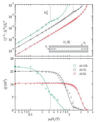
In this section, we experimentally confirm the existence of the proximity effect between the Al and the Nb layers and show this effect is controllable by varying the thickness of the Al layer. For this, we investigate how a magnetic field parallel to the microwave current dependence of and change as we tune the thickness of the Al layer. Figure 4 shows how the thickness of the Al layers affects the dependence of . Note that, as the thickness of the Al layers increases, starts to drop at a lower field, which already indicates the existence of the proximity effect.
In addition, as already mentioned in Sec. IV, becomes higher as the thickness of the Al layers increases. The origin of higher after Al cladding is probably less-lossy surface oxide or an improved interface between the substrate and the film. Thermal quasiparticles are not relevant because, at the measurement temperature (20 mK), thermal quasiparticles are expected to be frozen out.
For quantitative analysis of the proximity effect, we characterize the dependence of and in Fig. 4 using a set of parameters, which we call loss parameters, associated with magnetic field induced quasiparticle generation. The basis of this approach is that the magnetic field dependence of the real and imaginary parts of the complex resistivity can be studied via and as a function of field, respectively kwon . We emphasize that these loss parameters, shown in Table 4, were obtained purely by comparing the measured and expected and without incorporating any other types of measurements. To calculate the expected and as a function of , we need to model the complex resistivity kwon .
In order to model the complex resistivity associated with quasiparticle generation, the anisotropic GL equations were used because the trilayer resonators are anisotropic systems. (See Sec. S1 for details on the implementation of the anisotropic GL equations.) In this case, the penetration depth must be defined based on the direction of the magnetic field penetration as shown in the inset of Fig. 4. The GL coherence lengths along the in-plane and out-of-plane also need to be distinguished. Consequently, we have two GL parameters, () and (). Here, provides the relation . Once the anisotropic GL equations were implemented, the expected and as a function of were calculated following the procedure described in Sec. S2. During the calculation, we treated the trilayer as a single anisotropic layer with the thickness of the whole trilayer. Therefore, the loss parameters of Al-5L and Al-10L are effective parameters.
The measured data and calculated curves agree well (Fig. 4). This suggests that our system can be treated as a single system with effective parameters, and we should not strongly separate Nb and Al layers in our system. The reason for this is that the Al thickness is well below the coherence length of both Nb and Al. If there is a phase transition from superconducting Al/superconducting Nb to normal Al/superconducting Nb, then there must be some abrupt change in the dependence other than vortex injection, but no such a signature was observed.
In Table 4, and decrease as the Al thickness increases. This result is consistent with previous reports zhao1999 ; wang2000 ; brammertz2001 ; brammertz2002 . Note that of Al-5L is longer than that of Al-0L, although the proximity effect is expected to reduce (Refs. zhao1999, ; wang2000, ). This elongation of is likely due to electron scattering at the interface wang2000 . As the Al layer becomes thicker, the contribution of the Al layer to becomes dominant compared with the interface. As a result, of Al-10L is significantly shorter than that of Al-5L.
Note that, in Table 1, of Al-5L is about 0.1 GHz lower than that of Al-0L. In addition, of Al-10L is 0.1 GHz higher than that of Al-5L. Since is proportional to , where is the effective inductance per unit length, 0.1 GHz change in means 2% change in . In our geometry, the dominant contribution to is the inductance from the energy stored as an electromagnetic field . From the simulationkwon , we obtain nH/m, suggesting that 0.1 GHz change in corresponds to about 10 nH/m change in . The kinetic inductance per unit length can be calculated using the following formulakwon ; schmidt :
| (1) |
where is the cross-sectional area of the resonator. Using in Table 4 and from the simulation, we obtain the following values of : 10 nH/m for Al-0L; 13 nH/m for Al-5L; and 2.5 nH/m for Al-10L. These results suggest that the difference in of Al-5L and Al-10L is due to the reduction of the kinetic inductance, i.e., the penetration depth, by thicker Al cladding. However, the difference in of Al-0L and Al-5L is not easy to understand. The Al-Nb interface might contribute to the inductance, but the mechanism is unclear.
Lastly, from Fig. 4, we found that 5 nm Al-cladding is a good choice for applications in X-band ESR of 2 electron spin systems, which require a magnetic field of about 0.35 T. However, if the film thickness or the film quality of the Nb layers is significantly different from that of Al-0L, then the optimal thickness of the Al layer may vary.
VI Conclusion
In conclusion, we found that nonlinear responses of pure Nb microstrip resonators were induced by local Joule heating, while that of Al-clad resonators was induced by global heating. This qualitative change in nonlinear responses was likely due to Al current bypasses whose superconductivity is strengthened by the proximity effect between the Al and the Nb layers. This proximity effect was found to be controllable by tuning the Al layer thickness: as the thickness of the Al layer increases, , , and decrease. Improving the film quality enhanced the microwave critical current density, but it did not result in a qualitative change in nonlinear responses. Thus, our study showed that Al cladding is an effective way to eliminate nonlinear responses induced by local Joule heating, resulting in improved microwave power handling capability.
Strong microwave power handling capability will allow us to control spins or solid-state qubits efficientlysamkharadze2016 ; kroll2019 . Hence, this work will be useful for magnetic resonance applications as well as quantum information processing.
Supplementary Material
See the supplementary material for details regarding solving the anisotropic GL equations (Sec. S1), extracting the loss parameters (Sec. S2), and magnetic hysteresis in a finite (Sec. S3). curves at various in a modest are shown in Fig. S3.
Acknowledgements.
S.K. thanks to Ivar A. J. Taminiau and George Nichols for technical support, and Shinyoung Lee for helpful discussions. This work is supported by the Canada First Research Excellence Fund, the Canada Excellence Research Chairs (grant No. 215284), the Natural Sciences and Engineering Research Council of Canada (grant Nos. RGPIN-418579 and RGPIN-04178), and the Province of Ontario. The University of Waterloo’s Quantum NanoFab was used for this work. This infrastructure is supported by the Canada Foundation for Innovation, the Ontario Ministry of Research & Innovation, Industry Canada, and Mike & Ophelia Lazaridis.References
- (1) J. Zmuidzinas, Superconducting Microresonators: Physics and Applications, Annu. Rev. Condens. Matter Phys. 3, 169 (2012).
- (2) Z.-L. Xiang, S. Ashhab, J. Q. You, and F. Nori, Hybrid Quantum Circuits: Superconducting Circuits Interacting with Other Quantum Systems, Rev. Mod. Phys. 85, 623 (2013).
- (3) G. Kurizki, P. Bertet, Y. Kubo, K. Mølmer, D. Petrosyan, P. Rabl, and J. Schmiedmayer, Quantum Technologies with Hybrid Systems, Proc. Natl. Acad. Sci. U.S.A. 112, 3866 (2015).
- (4) O. W. B. Benningshof, H. R. Mohebbi, I. A. J. Taminiau, G. X. Miao, and D. G. Cory, Superconducting Microstrip Resonator for Pulsed ESR of Thin Films, J. Magn. Reson. 230, 84 (2013).
- (5) H. Malissa, D. I. Schuster, A. M. Tyryshkin, A. A. Houck, and S. A. Lyon, Superconducting Coplanar Waveguide Resonators for Low Temperature Pulsed Electron Spin Resonance Spectroscopy, Rev. Sci. Inst. 84, 025116 (2013).
- (6) A. J. Sigillito, H. Malissa, A. M. Tyryshkin, H. Riemann, N. V. Abrosimov, P. Becker, H.-J. Pohl, M. L. W. Thewalt, K. M. Itoh, J. J. L. Morton, A. A. Houck, D. I. Schuster, and S. A. Lyon, Fast, Low-Power Manipulation of Spin Ensembles in Superconducting Microresonators, Appl. Phys. Lett. 104, 222407 (2014).
- (7) C. Grezes, B. Julsgaard, Y. Kubo, M. Stern, T. Umeda, J. Isoya, H. Sumiya, H. Abe, S. Onoda, T. Ohshima, V. Jacques, J. Esteve, D. Vion, D. Esteve, K. Mølmer, and P. Bertet, Multimode Storage and Retrieval of Microwave Fields in a Spin Ensemble, Phys. Rev. X 4, 021049 (2014).
- (8) A. Bienfait, J. J. Pla, Y. Kubo, M. Stern, X. Zhou, C. C. Lo, C. D. Weis, T. Schenkel, M. L. W. Thewalt, D. Vion, D. Esteve, B. Julsgaard, K. Mølmer, J. J. L. Morton, and P. Bertet, Reaching the Quantum Limit of Sensitivity in Electron Spin Resonance, Nat. Nanotechnol. 11, 253 (2016).
- (9) C. Eichler, A. J. Sigillito, S. A. Lyon, and J. R. Petta, Electron Spin Resonance at the Level of Spins Using Low Impedance Superconducting Resonators, Phys. Rev. Lett. 118, 037701 (2017).
- (10) A. J. Sigillito, A. M. Tyryshkin, T. Schenkel, A. A. Houck, and S. A. Lyon, All-electric control of donor nuclear spin qubits in silicon, Nat. Nanotech. 12, 958 (2017).
- (11) S. Probst, A. Bienfait, P. Campagne-Ibarcq, J. J. Pla, B. Albanese, J. F. Da Silva Barbosa, T. Schenkel, D. Vion, D. Esteve, K. Mølmer, J. J. L. Morton, R. Heeres, and P. Bertet, Inductive-detection electron-spin resonance spectroscopy with 65 spins/ sensitivity, Appl. Phys. Lett. 111, 202604 (2017).
- (12) I. Kovacic and M. J. Brennan eds., The Duffing Equation: Nonlinear Oscillators and Their Behaviour (Wiley, 2011).
- (13) J. H. Oates, R. T. Shin, D. E. Oates, M. J. Tsuk and P. P. Nguyen, A nonlinear transmission line model for superconducting stripline resonators, IEEE Trans. Appl. Supercond. 3, 17 (1993).
- (14) E. A. Tholén, A. Ergül, K. Stannigel, C. Hutter, and D. B. Haviland, Parametric amplification with weak-link nonlinearity in superconducting microresonators, Phys. Scr. T137, 014019 (2009).
- (15) J. Ku, V. Manucharyan, and A. Bezryadin, Superconducting nanowires as nonlinear inductive elements for qubits, Phys. Rev. B 82, 134518 (2010).
- (16) L. J. Swenson, P. K. Day, B. H. Eom, H. G. Leduc, N. Llombart, C. M. McKenney, O. Noroozian, and J. Zmuidzinas, Operation of a titanium nitride superconducting microresonator detector in the nonlinear regime, J. Appl. Phys. 113, 104501 (2013).
- (17) H. R. Mohebbi, O. W. B. Benningshof, I. A. J. Taminiau, G. X. Miao, and D. G. Cory, Composite Arrays of Superconducting Microstrip Line Resonators, J. Appl. Phys. 115, 094502 (2014).
- (18) I. N. Hincks, C. E. Granade, T. W. Borneman, and D. G. Cory, Controlling Quantum Devices with Nonlinear Hardware, Phys. Rev. Applied 4, 024012 (2015).
- (19) A. Vl. Gurevich and R. G. Mints, Self-heating in normal metals and superconductors, Rev. Mod. Phys. 59, 941 (1987).
- (20) T. Jacobs, B. A. Willemsen, and S. Sridhar, Quantitative analysis of nonlinear microwave surface impedance from non‐Lorentzian resonances of high Q resonators, Rev. Sci. Instrum. 67, 3757 (1996).
- (21) J. Wosik, L.-M. Xie, K. Nesteruk, D. Li, J. H. Miller, Jr., and S. A. Long, Power Handling Capabilities of Superconducting YBCO Thin Films: Thermally Induced Nonlinearity Effects, J. Supercond. 10, 97 (1997).
- (22) J. Wosik, L.-M. Xie, R. Grabovickic, T. Hogan, and S. A. Long, Microwave Power Handling Capability of HTS Superconducting Thin Films: Weak Links and Thermal Effects Induced Limitation, IEEE Trans. Appl. Supercond. 9, 2456 (1999).
- (23) A. J. Purnell, L. F. Cohen, H. Y. Zhai, H. M. Christen, M. P. Paranthaman, D. H. Lowndes, L. Hao, and J. C. Gallop, Nonlinear microwave response of an MgB2 thin film, Supercond. Sci. Technol. 17, 681 (2004).
- (24) B. Abdo, E. Sergev, O. Shtempluck, and E. Buks, Nonlinear dynamics in the resonance line shape of NbN superconducting resonators, Phys. Rev. B 73, 134513 (2006).
- (25) J. Wosik, L.-M. Xie, and R. Grabovickic, Thermal Effects in Microwave Current-Induced Weak Link Switching in YBCO Thin Films, Supercond. Sci. Technol. 22, 105003 (2009).
- (26) G. Ghigo, R. Gerbaldo, L. Gozzelino, F. Laviano, G. Lopardo, E. Monticone, C. Portesi, and E. Mezzetti, Local Thermal Bistability in MgB2 Microwave Coplanar Resonators: Opposite Jumpwise Response to Weak-Link Switching and to Vortex Avalanches, Appl. Phys. Lett. 94, 052505 (2009).
- (27) G. Ghigo, R. Gerbaldo, L. Gozzelino, F. Laviano, and E. Mezzetti, Switching response of MgB2 thin-film microwave resonators due to local nonlinear Joule heating, Phys. Rev. B 82, 054520 (2010).
- (28) M. W. Brenner, S. Gopalakrishnan, J. Ku, T. J. McArdle, J. N. Eckstein, N. Shah, P. M. Goldbart, and A. Bezryadin, Cratered Lorentzian response of driven microwave superconducting nanowire-bridged resonators: Oscillatory and magnetic-field induced stochastic states, Phys. Rev. B 83, 184503 (2011).
- (29) C. Kurter, A. P. Zhuravel, A. V. Ustinov, and S. M. Anlage Microscopic Examination of Hot Spots Giving Rise to Nonlinearity in Superconducting Resonators, Phys. Rev. B 84, 104515 (2011).
- (30) Y.-C. Tang, S. Kwon, H. R. Mohebbi, D. G. Cory, and G.-X. Miao, Phonon Engineering in Proximity Enhanced Superconductor Heterostructures, Sci. Rep. 7, 4282 (2017).
- (31) P. G. de Gennes, Superconductivity of Metals and Alloys (Westview Press, 1989).
- (32) B. Y. Jin and J. B. Ketterson, Artificial Metallic Superlattices, Adv. Phys. 38, 189 (1989).
- (33) M. R. Vissers, J. Gao, M. Sandberg, S. M. Duff, D. S. Wisbey, K. D. Irwin, and D. P. Pappas, Proximity-coupled Ti/TiN multilayers for use in kinetic inductance detectors, Appl. Phys. Lett. 102, 232603 (2013).
- (34) J. C. Cuevas, D. Roditchev, T. Cren, and C. Brun, in The Oxford Handbook of Small Superconductors, edited by A. V. Narlikar (Oxford University Press, 2017).
- (35) S. Kwon, A. Fadavi Roudsari, O. W. B. Benningshof, Y.-C Tang, H. R. Mohebbi, I. A. J. Taminiau, D. Langenberg, S. Lee, G. Nichols, D. G. Cory, and G.-X. Miao, Magnetic Field Dependent Microwave Losses in Superconducting Niobium Microstrip Resonators, J. Appl. Phys. 124, 033903 (2018).
- (36) J. M. Sage, V. Bolkhovsky, W. D. Oliver, B. Turek, and P. B. Welander, Study of Loss in Superconducting Coplanar Waveguide Resonators, J. Appl. Phys. 109, 063915 (2011).
- (37) D. E. Oates, A. C. Anderson, and P. M. Mankiewich, Measurement of the surface resistance of YBa2Cu3O7-x thin films using stripline resonators, J. Superconduct. 3, 251 (1990).
- (38) T. L. Hylton, A. Kapitulnik, M. R. Beasley, J. P. Carini, L. Drabeck, and G. Grüner, Weakly coupled grain model of high‐frequency losses in high superconducting thin films, Appl. Phys. Lett. 53, 1343 (1988).
- (39) T. L. Hylton and M. R. Beasley, Effect of grain boundaries on magnetic field penetration in polycrystalline superconductors, Phys. Rev. B 39, 9042 (1989).
- (40) J. Halbritter, RF Residual Losses, Surface Impedance, and Granularity in Superconducting Cuprates, J. Appl. Phys. 68, 6315 (1990).
- (41) J. Halbritter, On Extrinsic Effects in the Surface Impedance of Cuprate Superconductors by Weak Links, J. Appl. Phys. 71, 339 (1992).
- (42) J. Halbritter, Granular Superconductors and Their Intrinsic and Extrinsic Surface Impedance, J. Supercond. 8, 691 (1995).
- (43) C. C. Chang, M. Gurvitch, D. M. Hwang, and C. W. Blonder, Auger electron spectroscopy, transmission electron microscopy, and scanning electron microscopy studies of Nb/Al/Nb Josephson junction structures, J. Appl. Phys. 61, 5089 (1987).
- (44) J. Halbritter, On the Oxidation and on the Superconductivity of Niobium, Appl. Phys. A 43, 1 (1987).
- (45) J. Halbritter, Low Temperature Oxidation of Nb and of Nb-compounds in Relation to Superconducting Application, J. Less-Common Met. 139, 133 (1988).
- (46) A. V. Feshchenko, O.-P. Saira, J. T. Peltonen, and J. P. Pekola, Thermal Conductance of Nb Thin Films at Sub-kelvin Temperatures, Sci. Rep. 7, 41728 (2017).
- (47) J. Gittleman, B. Rosenblum, T. E. Seidel, and A. W. Wicklund, Nonlinear Reactance of Superconducting Films, Phys. Rev. 137, A527 (1965).
- (48) C.-W. Lam, D. M. Sheen, S. M. Ali, and D. E. Oates, Modeling the Nonlinearity of Superconducting Strip Transmission Lines, IEEE Trans. Appl. Supercond. 2, 58 (1992).
- (49) J. R. Clem and V. G. Kogan, Kinetic Impedance and Depairing in Thin and Narrow Superconducting Films, Phys. Rev. B 86, 174521 (2012).
- (50) M. A. Golosovsky, H. J. Snortland, and M. R. Beasley, Nonlinear Microwave Properties of Superconducting Nb Microstrip Resonators, Phys. Rev. B 51, 6462 (1995).
- (51) S. P. Zhao and Q. S. Yang, Penetration Depth in Conventional Layered Superconductors: A Proximity-Effect Model, Phys. Rev. B 59, 14630 (1999).
- (52) R. F. Wang, S. P. Zhao, G. H. Chen, and Q. S. Yang, Magnetic Penetration Depth in Nb/Al and Nb/Cu Superconducting Proximity Bilayers, Phys. Rev. B 62, 11793 (2000).
- (53) G. Brammertz, A. Poelaert, A. A. Golubov, P. Verhoeve, A. Peacock, and H. Rogalla, Generalized proximity effect model in superconducting bi- and trilayer films, J. Appl. Phys. 90, 355 (2001).
- (54) G. Brammertz, A. Poelaert, A. A. Golubov, P. Verhoeve, R. den Hartog, A. Peacock, and H. Rogalla, Critical temperature of superconducting bilayers: Theory and experiment, Appl. Phys. Lett. 80, 2955 (2002).
- (55) T. Matsushita, Flux Pinning in Superconductors, 2nd ed. (Springer, 2014).
- (56) V. V. Schmidt, The Physics of Superconductors (Springer, 1997), Sec. 2.6.
- (57) N. Samkharadze, A. Bruno, P. Scarlino, G. Zheng, D. P. DiVincenzo, L. DiCarlo, and L. M. K. Vandersypen, High-Kinetic-Inductance Superconducting Nanowire Resonators for Circuit QED in a Magnetic Field, Phys. Rev. Applied 5, 044004 (2016).
- (58) J. G. Kroll, F. Borsoi, K. L. van der Enden, W. Uilhoorn, D. de Jong, M. Quintero-Pérez, D. J. van Woerkom, A. Bruno, S. R. Plissard, D. Car, E. P. A. M. Bakkers, M. C. Cassidy, and L. P. Kouwenhoven, Magnetic-Field-Resilient Superconducting Coplanar-Waveguide Resonators for Hybrid Circuit Quantum Electrodynamics Experiments, Phys. Rev. Applied 11, 064053 (2019).
See pages 1 of supp.pdf
See pages 2 of supp.pdf
See pages 3 of supp.pdf
See pages 4 of supp.pdf
See pages 5 of supp.pdf
See pages 6 of supp.pdf