Spectra Analysis to Stretching of ADB Structure Metamaterial
Abstract
Asymmetric-double-bars (ADB) structure is one of the most interesting plasmonic metamaterials that has been broadly investigated. Here we propose to manufacture ADB on top of elastic material, to get direct control to the dimension of ADB elements. To analyze the spectra numerically, simulation by commercial software (COMSOL) are carried out. We successfully modify the characteristic spectra and enhance Q-factor of the peak near infrared by introducing angular and amplitude parameters of the stretching of substrate in the simulation. At the mean time, we significantly restrain red shift in the absorption spectra by applying flipped-configuration and substrate etching configuration to ADB structure. Intriguing quadratic functions between stretching ratio and the absorption peak wavelength are obtained when stretching in x and y direction. For other directions, EIT lineshape appears in transmission spectra. These results might contribute to future application of plasmonic metamaterial in laser controlling and sensors.
In nature, most plasmonic materials don’t have strong interaction with the magnetic component of light. With the development of nanotechnology, plasmonic metamaterial, usually formed by metal array in nanoscale, came into sight and rapidly developed for its artificial magnetism at optical frequencies. With further researches, plasmonic metamaterial gives out many possible intriguing properties, such as negative refraction index material negative1 ; negative2 ; negative3 ; negative4 , extraordinary transmission trans1 ; trans2 , and a lot more possibilities. Much effort has been made to explain this phenomenon. The widely accepted explanation to these features is the surface plasmons (SPs) theory wikisps . Studies have shown that metals such as Au and Pt EIT7 are unique in that they can enhance the magnetic field near the surface, resulting in some characteristic spectrum.
Many possible configurations of plasmonic metamaterial have been developed, for example split rings split1 ; split2 ; split3 ; split4 , has been found related with intriguing properties. Another important structure is asymmetric-double-bars(ADB)adb1 , which is mainly investigated in this paper. One element of ADB matrix consists of two bars, slightly different in length. It is one of the simplest structures in metamaterials, resulting in relatively easy manufacture and simulation. ADB is also promising for realizing sharp Fano resonance fano1 ; fano2 ; fano3 . A quadrupole-like dark mode with small radiative loss is excited by a free space electromagnetic wave because of asymmetry of the ADB. It consists of two dipoles with opposite phases, and Fano interference occurs between the quadrupole mode and the dipole mode. A net dipole moment is small, which leads to weak radiative loss and high Q-factors. Therefore, ADB structure is applicable in many occasions, for example, possibility of electromagnetically induced transparency (EIT) EIT1 ; EIT2 ; EIT3 ; EIT4 ; EIT5 ; EIT6 ; EIT7 , and modification to the fluorescence spectrum of coupled Quantum Dots OMwithQD .
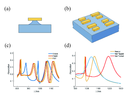
In our model, we use ADB formed by gold for high electrical conductance. It has been found out that alternately flipping the ADB structure, that is to make the adjacent elements to be head-to-head rather than head-to-tail, can enhance the quality factor of the absorption spectra, according to previous work by Yuto Moritake et al. anti . Since the dipole-dipole interaction in the non-flipped structure can be undesirably affected from outside of the periodic structure, alternately flipping can prevent this and enhance the should-be interaction and increase the Q-factor. Another problem in nanostructure fabrication is to reduce the influence to the electric and magnetic field by the substrate. The reduction of substrate influence can be achieved by using selective and isotropic etching of the substrate as demonstrated in foat . Substrate etching was applied to a silicon substrate under the gold nanostructures shown as FIG.1(a). And it was experimentally proved that it can prevent the red shift and improve the refractive index sensitivity based on far field interference. However, the decrease in the Q-factors of the Fano resonance is observed after applying substrate etching, which is due to the electric field distortion by a closely placed substrate. In our experiment, we combine the alternately flipped configuration of ADB and substrate etching together in order to achieved the finest spectral properties of Fano resonance.
The schematics of configuration is shown as FIG.1(b). The unit cell of the ADB is composed of two gold bars of which the size is l1=280 nm, l2=200 nm, and width w=100 nm, gap between two bars w=100 nm, height h=50 nm. The periodic lengths in x,y directions are both 500 nm, and four alternately-flipped ADB units are placed symmetrically in four quadrants of square. Substrate etching is also applied in our design, which is estimated to be 25 nm during simulation. In experiment, we suggest coating another 5 nm Ti between gold bar and the silicon dioxide to improve the adhesive strength, which is not shown in this figure.
Previous fabrication of ADB metamaterial was always conducted on silicon dioxide, because of its high transparency to all colors of light, endurance to laser and stable chemistry property. Yet silicon dioxide retains the possibility of being elastic to change the period and the distance, which means that one piece of sample corresponds to one spectra. In order to improve the flexibility of the experiment, the substrate will have to meet the requirement mentioned above, and have the controllable flexibility. Piezoelectric material and thermal expansion material share the flexibility but the degree of relative deformation of the former is too small and the direction of expansion of the latter can hardly be controlled. Thus, we try to achieve this goal by mechanically manipulating suitable elastic plastic. According to the description above, we think that Polyethylene Terephthalate (PET) and Polyether Ether Ketone (PEEK) are both worth expecting candidates. However, it might require more stringent conditions to EBL process, which will not be discussed any further in this paper.
Here we present our simulation result based on the finite element method (FEM) by commercial software COMSOL. As is shown in FIG.1 (c), we perform spectra analysis of the designed ADB structure on different substrates, including silicon dioxide, PET and PEEK. There are three absorption peaks for silicon dioxide. We observe the spatial magnetic field around ADB and find the interaction between dark mode and bright mode similar with each other. Four peaks for PET and PEEK are observed, and it looks like the two peaks on the right derive from the right one of silicon dioxide spectra. Considering the difference on reflective index molecular structure, it’s not surprising to see the difference. And it is possible to make use of these two peaks for higher Q-factor. To clarify, we name the right peak on the silicon dioxide absorption spectra to be R peak. What’s important is, we observe the similar reaction of two-peaks (from PET and PEEK) compared with R peak in the stretching process, including the separation of peaks, which means the one-peak becomes two-peak, and the two-peak becomes four-peak. We will come to this part soon. Hereby, we will take more look into to the R peak on silicon dioxide spectra.
As shown in FIG.1 (d), we also run simulation to prove the reasonability of alternately flipped configuration and substrate etching. Yellow line refers to alternately flipped configuration with substrate etching, and red line and blue line refer to alternately flipped configuration without substrate etching and non-flipped configuration with substrate etching, respectively. It is observed from the spectra that flipping unit cells would create a sharper peak and substrate etching would eliminate red shift. Alternately flipped configuration with substrate etching, which combined both advantages, would have a sharper peak than non-flipped configuration with substrate etching and much weaker red shift compare with alternately flipped configuration without substrate etching.
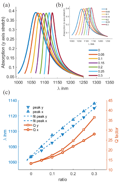
In order to characterize the stretch, we set two parameters in the model. means angle between the stretching direction and x axis, and Ratio means the rate of increase in the specific direction. First of all we can see the spectra modification when or 0, that is y and x direction, as is shown in FIG.2 (a) and (b), which means in y and x axis, respectively. Different lines represents different Ratio. And we can see the R peak tends to be continuously red shifting, and FWHM increasing, as Ratio grows. We can consider the enlargement of space between the two bars is like that of an optical cavity. By pulling the two bars away from each other, the resonance wavelength is to red shift. Here the effect of head-to-head structure is also weakened, thus the red shift isn’t suppressed.
To describe the red shift and change in FWHM, we find peaks shown in FIG.2 (a) and (b) and plot them with Ratio, which is shown in FIG.2 (c). Y-axis on the left refers to R peak wavelength, on the right is the Q-factor, and , where is FWHM. Monotone increasing is observed. Then we use the quadratic function to fit the curve of the peak to ratio, as is also shown in figure FIG.2. In order to explain that, we can regards ADB structure as an optical cavity, and the eigen-wavelength should be proportional to cavity length as a result. And we can see that when Ratio is from 0 to 0.2, linear distribution is obvious; yet other factors will introduce higher order terms, as the quadratic function we use to fit indicates second-order term. These nonlinear terms come from various causes, for example, the impact caused by flipped structure should decrease in a quadratic way as Ratio goes up, and if the double bars get too close or too far-away, it will also introduce nonlinear term. The second-order approximation can work fine when Ratio is smaller than 0.3, which is most likely to happen in future applications.
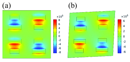
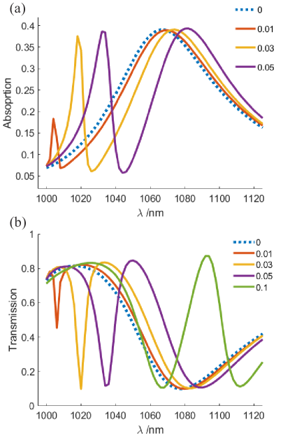
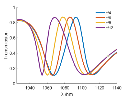
We also study on different angles, for example , and interesting modification is discovered. If we set the parameter , and scan Ratio, an EIT lineshape appears, as in FIG.3 (b). When Ratio is small, a small peak in the absorption spectra, near R peak, begins to grow with Ratio. As Ratio becomes big enough (), the little peak becomes as big as R peak. And if we see FIG.3 (a), the transmission spectra, the characteristic lineshape of EIT is shown. We may consider the small peak help generate a metastable state near the fano resonance peak, and the small peak comes from the disruption of symmetry between two bars. ADB structure in our design have an axis of symmetry. And stretching in an angle like breaks this sysmmetry, and introduce a bias of the bright mode in spatial distribution, which has influence on the coupling between the bright mode and the dark mode. According to FIG.4, the spatial distribution of Hz have changed. Moreover, the peaks continues to red shift with the growing of Ratio, which is estimated before. If we set Ratio constant, and scan , it will introduce more nonlinear effects, which makes the analysis less applicable. However, when Ratio is 0.1 and nonlinear effects are unnoticeable in this particular region, it seems that the transmission has give out some hints for future investigation. And in other region, nonlinear effects are strong, which makes the scanning of less useful. But when is close to or 0, the difference in spectra is ignorable, which means it’s not to sensitive to direction error in future application.
In conclusion, plasmonic metamaterial is becoming more and more important in scientific investigation for its potential in improving quality factor of sensors and quantum dots and so on. Adjusting the plasmonic metamaterial in ADB structure with one piece is tempting, which might bring great effect to this industry. We run simulation on silicon dioxide and set two important parameters, Ratio and , to represent the stretching on the substrate. When equals to or 0, the R peak wavelength is the function of Ratio, which is well fitted by quadratic function. An increasing Q-factor is also observed. When we set to be , and scan Ratio, EIT lineshape in transmission spectra appears for the breaking of structure symmetry. This phenomenon is also observed when is at other values. And when we set Ratio constant and scan the other way, nonlinear effects will take over and when is small, the effects are negligible. All phenomenon mentioned above are seen in PET and PEEK spectra as well. By doing so, we see the chance of manipulating plasmonic metamaterial by using elastic substrate. They could have various applications, for example, tuning the emission wavelength of fluorescence by quantum dots like PbS and graphene, and the possibility of willingly adjustment of near-monochrome beam.
We would like to thank researcher Kun Zhang and Dianfa Zhou from USTC Center for Micro- and Nanoscale Research and Fabrication, for their experimental help in our fabrication of plasmonic metamaterial; we also thank Prof. Zhongping Wang for his instructions throughout our experiment. We acknowledge Tanwei Li and Jian Zuo from USTC Physical and chemical science laboratory center for providing consultation to our experiment.
References
- (1) Shelby R. A., Smith D. R., Schultz S., Science, 292(5514), 77 (2001).
- (2) D. R. Smith, J. B. Pendry, M. C. K. Wiltshire, Metamaterials and Negative Refractive Index
- (3) Shalaev, V. M. Optical negative-index metamaterials. Nat. Photon. 1, 41–48 (2007).
- (4) C. García-Meca et al. Opt. Express 17, 6026-6031 (2009)
- (5) X. R. Jin, J. Park, H. Zheng, S. Lee, Y. Lee, J. Y. Rhee, K. W. Kim, H. S. Cheong, and W. H. Jang, “Highly-dispersive transparency at optical frequencies in planar metamaterials based on two-bright-mode coupling,” Opt. Express 19(22), 21652–21657 (2011).
- (6) H. W. Gao, J. Henzie, and T. W. Odom, “Direct evidence for surface plasmon-mediated enhanced light transmission through metallic nanohole arrays,” Nano Lett. 6, 2104 (2006).
- (7)
- (8) J. Zhou, T. Koschny, M. Kafesaki, E. N. Economou, J. B. Pendry, and C. M. Soukoulis, “Saturation of the magnetic response of split-ring resonators at optical frequencies,” Phys. Rev. Lett. 95, 223902 (2005).
- (9) Katsarakis, N., Koschny, T., Kafesaki, M., Economou, E. N. Soukoulis, C. M. Electric coupling to the magnetic resonance of split ring resonators. Appl. Pys. Lett. 84(15), 2943 (2004).
- (10) C. Rockstuhl, T. Zentgraf, H. Guo, N. Liu, C. Etrich, I. Loa, K. Syassen, J. Kuhl, F. Lederer, and H. Giessen, “Resonances of split-ring resonator metamaterials in the near infrared,” Appl. Phys. B 84, 219–227 (2006).
- (11) Fabrication of three dimensional split ring resonators by stress-driven assembly method
- (12) N. Verellen, Y. Sonnefraud, H. Sobhani, F. Hao, V. V. Moshchalkov, P. Van Dorpe, P. Nordlander, and S. A. Maier, “Fano resonances in individual coherent plasmonic nanocavities,” Nano Lett. 9(4), 1663–1667 (2009).
- (13) B. Luk’yanchuk, N. I. Zheludev, S. A. Maier, N. J. Halas, P. Nordlander, H. Giessen, and C. T. Chong, “The Fano resonance in plasmonic nanostructures and metamaterials,” Nat. Mater. 9(9), 707–715 (2010).
- (14) H. Liu, G. X. Li, K. F. Li, S. M. Chen, S. N. Zhu, C. T. Chan, and K. W. Cheah, “Linear and nonlinear Fano resonance on two-dimensional magnetic metamaterials,” Phys. Rev. B 84, 235437 (2011).
- (15) Hokari, Ryohei; Kanamori, Yoshiaki; Hane, Kazuhiro (2014): Comparison of electromagnetically induced transparency between silver, gold, and aluminum metamaterials at visible wavelengths. In Optics express 22 (3), pp. 3526–3537. DOI: 10.1364/OE.22.003526.
- (16) Xing-Ri Jin, Jinwoo Park, Haiyu Zheng, Seongjae Lee, YoungPak Lee, Joo Yull Rhee, Ki Won Kim, H. S. Cheong, and Won Ho Jang, OPTICS EXPRESS. 19, 22, 21652 (2011).
- (17) R. Hokari, Y. Kanamori, and K. Hane, “Fabrication of planar metamaterials with sharp and strong electromagnetically induced transparency-like characteristics at wavelengths around 820 nm,” J. Opt. Soc. Am. B 31(5), 1000–1005 (2014).
- (18) Z. -G. Dong, H. Liu, M. -X. Xu, T. Li, S. -M. Wang, S. -N. Zhu, and X. Zhang, “Plasmonically induced transparent magnetic resonance in a metallic metamaterial composed of asymmetric double bars,” Opt. Express 18, 18229 (2010).
- (19) Artar, A. A. Yanik, and H. Altug, “Multispectral plasmon induced transparency in coupled meta-atoms,” Nano Lett. 11(4), 1685–1689 (2011). 结构不一样,但是应该可以引用
- (20) S. Hu, H. Yang, S. Han, X. Huang, and B. Xiao, “Tailoring dual-band electromagnetically induced transparency in planar metamaterials,” Appl. Phys. Lett. 117(4), 043107 (2015).
- (21) Niakan et al. J. Opt. Soc. Am. B 232, Vol. 29, No. 9 (2012).
- (22) Yuto Moritake et al. OPTICS EXPRESS 26. 3674 (2018).
- (23) Yuto Moritake et al. Appl. Phys. Lett. 107, 211108 (2015)
- (24) Yuto Moritake, Y. et al. Sci. Rep. 6, 33208; doi: 10.1038/srep33208 (2016).
- (25) Yuto Moritake, Yoshiaki Kanamori, and Kazuhiro Hane, OPTICS LETTERS. 36, 4057 (2014).
- (26) S.D.Liu, Resonance and Application of Surface Plasmons on Metal Nanosystems, ISBN: 978-7-118-09218-9 (2013).
- (27) K. Tanaka, E. Plum, J. Y. Ou, T. Uchino, and N. I. Zheludev. Phys. Rev. Lett. 105, 227403 (2010)