Characterisation of AMS H35 HV-CMOS monolithic active pixel sensor prototypes for HEP applications
Abstract
Monolithic Active Pixel Sensors (MAPS) produced in High Voltage CMOS (HV-CMOS) technology are being considered for High Energy Physics applications due to the ease of production and the reduced costs. Such technology is especially appealing when large areas to be covered and material budget are concerned. This is the case of the outermost pixel layers of the future ATLAS tracking detector for the High Luminosity LHC. For experiments at hadron colliders, radiation hardness is a key requirement which is not fulfilled by standard CMOS sensor designs that collect charge by diffusion. This issue has been addressed by depleted active pixel sensors in which electronics are embedded into a large deep implantation ensuring uniform charge collection by drift. Very first small prototypes of hybrid depleted active pixel sensors have already shown a radiation hardness compatible with the ATLAS requirements. Nevertheless, to compete with the present hybrid solutions a further reduction in costs achievable by a fully monolithic design is desirable. The H35DEMO is a large electrode full reticle demonstrator chip produced in AMS HV-CMOS technology by the collaboration of Karlsruher Institut für Technologie (KIT), Institut de Física d’Altes Energies (IFAE), University of Liverpool and University of Geneva. It includes two large monolithic pixel matrices which can be operated standalone. One of these two matrices was characterised at beam test before and after irradiation with protons and neutrons. Results demonstrated the feasibility of producing radiation hard large area fully monolithic pixel sensors in HV-CMOS technology. H35DEMO chips with a substrate resistivity of irradiated with neutrons showed a radiation hardness up to a fluence of with a hit efficiency of about and a noise occupancy lower than hits in a LHC bunch crossing of at .
1 Introduction
Monolithic Active Pixel Sensors (MAPS) produced with CMOS process are becoming of great interest for High Energy Physics (HEP) experiments. In particular Depleted MAPS (DMAPS) first proposed in [1] give the possibility of having a fast monolithic detector with a large depleted region and reduced thickness for HEP applications. In DMAPS the signal is generated by charge drift instead of diffusion resulting in a faster charge collection with respect to normal MAPS and less prone to the effects of radiation damage. This technology is being investigated for the upgrade of the ATLAS detector at the High Luminosity Large Hadron Collider (HL-LHC) with the aim of covering large areas in the outer pixel layers of the Inner Tracker (ITk) using cost-effective detectors [2]. First prototypes of depleted active pixel sensors produced in H18 AMS [3] CMOS technology and capacitive coupled to ATLAS FE-I4 chips have already demonstrated to resists large radiation fluences and thus be interesting candidates for the LHC experiments [4]. The next step towards a final module for the ITk will be the development of a full scale monolithic prototype. The H35DEMO, was thus developed with the main purpose of demonstrating the feasibility of producing large area devices and investigate full size monolithic structures. For this first large area prototype the technology (H35) was chosen instead of the technology (H18) to contain production costs and investigate its use for less demanding radiation applications such as strip detectors.
2 The H35DEMO demonstrator
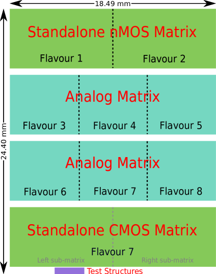
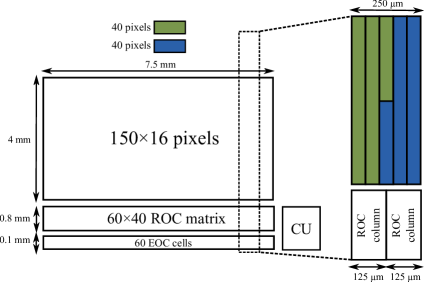
The H35DEMO [5] is a large area demonstrator chip produced in AMS High Voltage CMOS (HV-CMOS) technology on four different substrate resistivities: . The design was carried out by the collaboration of Karlsruher Institut für Technologie (KIT), Institut de Física d’Altes Energies (IFAE) and University of Liverpool. The layout of the chip, shown in figure 1, consists of four independent pixel matrices: two analog matrices of pixels meant to be capacitive coupled to ATLAS FE-I4 readout ASICS [6]; and two monolithic matrices of pixels including digital electronics in the periphery to be operated standalone. Additional passive test structures without electronics are present at the edge of the chip. In particular a pixel matrix for Transient Current Technique (TCT) studies was extensively measured before and after irradiation, and results have been published in ref. [7].
The total dimensions of the chip are . In all four matrices the pixel size is , the same as in the FE-I4. The sensor part is a p-n junction obtained by a Deep N-Well over a p-type substrate. Analog electronics are embedded and shielded inside the same Deep N-Well also acting as collecting electrode. The chip is produced with a single side process on thick wafers with P-Well rings surrounding the N-Wells on the top surface where the negative High Voltage (HV) for reverse bias is applied. The two analog matrices contain three different flavours of active pixels each combining the presence or the absence of additional bias rings between the Deep N-Wells, high or low gain, and Linear transistors (LT) or Enclosed Layout Transistors (ELTs). An extensive description and characterisation of these matrices can be found in ref. [8]. This paper will be dedicated to the characterisation of the monolithic part of the chip and in particular of the CMOS matrix. A detailed description of analog and digital architectures of the standalone matrices can be found in refs. [5, 9]. In the following only the characteristics relevant to the presented measurements will be discussed.
2.1 The monolithic CMOS matrix
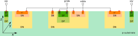
The pixels of the monolithic CMOS matrix combine high gain and LT without employing additional Deep P-Wells under the P-Well rings, as the pixels in the central columns of the second analog matrix (flavour 7). Layout and cross section of a pixel cell are shown in figure 2. The Deep N-Well is divided into three parts to reduce the total capacitance of the pixel maintaining an uniform depletion of the bulk. The analog electronics are embedded in the central well and mainly include a Charge Sensitive Amplifier (CSA), a shaper and a second stage amplifier.
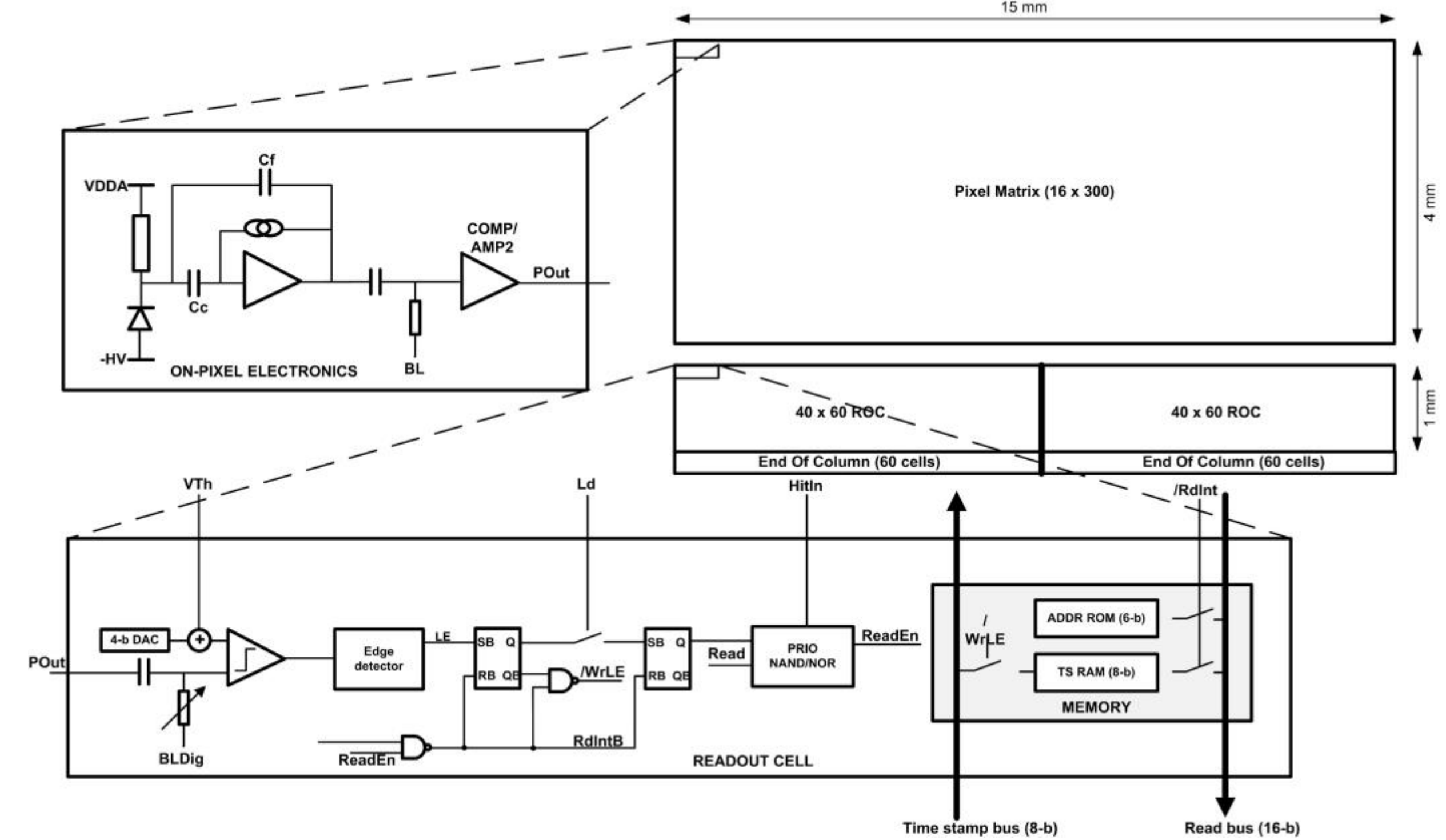
A sketch of the pixel and the periphery arrangement including block diagrams of the analog and digital electronics is shown in figure 3. Each pixel is connected to a digital ReadOut Cell (ROC) placed in the periphery of the matrix where the response of the analog stage is processed. The ROCs are divided into two blocks arranged in matrices of 60 columns and 40 rows such that each ROC column is connected to two and a half columns of analog pixels. In the ROC a CMOS comparator is implemented to discriminate the signal generated by a crossing particle from the noise. When the signal crosses the comparator threshold, column, row and time-stamp relative to the threshold crossing time are stored. The right part of the matrix, i.e. columns from 150 to 299, includes an additional CMOS comparator. This can be set to a lower threshold to generate a second time-stamp which is stored only if the signal passed the threshold of the first comparator. The aim of this scheme is to improve the timing performance by reducing the size of the time-walk effect. The digital readout of the pixel matrix implements a column drain architecture with priority encoding where the information in the highest row is the first to be sent to the End Of Column (EOC). Data from the left most column of each half matrix is then serialised and sent out of the chip at the clock speed without zero suppression.
2.2 The monolithic NMOS matrix
The monolithic NMOS matrix integrates comparators made of NMOS transistors directly on pixel. The pixels in the left half of the matrix, consisting of columns from 0 to 149, employ standard NMOS comparators, while the pixels in the right half, columns 150 to 299, include more complex NMOS comparators to compensate for time walk by making the propagation time independent of the amplitude of the input signal. Due to the space occupied by the additional electronics inside the pixel, the Deep N-Well is not separated as in the other matrices, leading to a larger capacitance. The digital front-end in the ROC is the same as in the left part of the CMOS matrix. In this case the CMOS comparators in the periphery allow to translate the low voltage output levels of the NMOS comparators to CMOS signals for the digital electronics.
3 The readout system
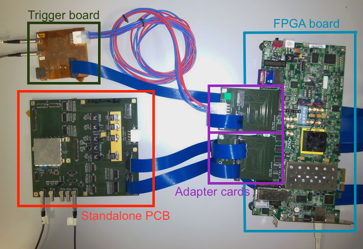
A Data Acquisition (DAQ) system dedicated to read out the monolithic matrices of the H35DEMO chip was developed at IFAE, Barcelona and is shown in figure 4. The hardware is based on the Xilinx ZC706 FPGA development board222Xilinx: All Programmable, [https://www.xilinx.com] and a custom designed carrier board where the chip is attached and wire-bonded. This, so called Standalone PCB, includes low voltage regulators to power the different matrices of the chip and Low Voltage Differential Signaling (LVDS) for communications. Through the Standalone PCB it is possible to apply the bias to the junction, provide an external test pulse for characterisation and tuning, and monitor the analog output of the CSA of pixel in the first column of both NMOS and CMOS matrices. Additional pins and connections on the board are implemented to monitor different signals of the chip for debugging purposes.
A first version of the Standalone PCB was produced which allowed to fully wire-bond and program the two monolithic matrices only. In this configuration the leakage current of the sensor was observed to be of the order of milliamps due to floating potentials in the pixels of the analog matrices. Even if it was possible to operate non-irradiated chips in these conditions, such large leakage current becomes particularly critical for irradiated devices due to the risk of thermal runaway. The problem was solved with the design of a second version of the Standalone PCB allowing for wire-bonding and programming of the analog matrices. All the presented results were obtained using this second version of the standalone PCB with the exception of the non-irradiated chip which was measured at beam tests on the first version of the standalone PCB.
A Trigger Board was developed to add external trigger capabilities to the system enabling integration with particle tracking telescopes for beam test measurements. This board consists of one LEMO connector to accept TTL trigger input signals and a second LEMO connector used to deliver a TTL busy signal. Both connectors are terminated on . A trigger-busy scheme is used to synchronise the H35DEMO data taking with an external DAQ reference system: After receiving a trigger pulse the H35DEMO DAQ system issues a busy signal to prevent the external reference system to further process and send triggers until all data of the H35DEMO is readout and processed. The same functions can be alternatively delegated to an RJ45 connector also present on this board. The DAQ is completed by a series of FMC adapter cards enabling connections between the FPGA board and the other components of the system.
A H35DEMO specific FPGA firmware was developed for the Xilinx board which allows to program the shift registers of all four pixel matrices independently and operate one of the two monolithic matrices at the time in continue acquisition mode or in trigger acquisition mode. In the trigger acquisition mode three parameters (trigger delay, event block and dead time) can be tuned to define the time window in which the output data from the chip is stored following a trigger signal. The firmware also implements zero suppression and supports Direct Memory Access (DMA).
A software written in C++ and using a Graphical User Interface (GUI) written in QT 333Qt Group, www.qt.io is used to steer and synchronise the operations of the FPGA, the external power supplies, and the pulse generator, for debugging, tuning and data taking. It communicates with a server running on the on-board operating system of the ZC706 via ethernet connection using a TCP/IP protocol.
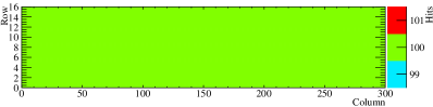
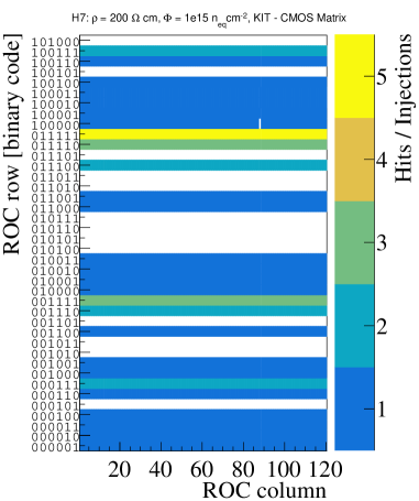
Examples of a test injection scan and a source scan obtained with this DAQ system for the CMOS monolithic matrix are shown in figure 5. In the test injection scan ulses per pixel are injected directly in the pre-amplifier while for the source scan the signal was generated by a radioactive source of beta electrons placed on top of the matrix.
4 Samples and irradiations
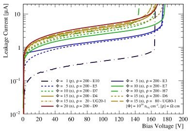
H35DEMO chips with resistivity substrate were irradiated with neutron in the TRIGA Mark II research reactor of the Jožef Stefan Institute (JSI) in Ljubljana [11] up to a fluence of and at the KIT Zyclotron [10] with protons up to a fluence of , equivalent to a Total Ionisation Dose (TID) of about . For neutron irradiations at JSI there is also a low TID of about per , which is due to gamma emission [12]. Two chips, one with a substrate resistivity of and one of were also irradiated with neutrons at JSI to . After irradiation all samples were subject to an average annealing due to shipping and handling of about 1 week at room temperature before being measured. A list of the available modules and correspondent irradiation fluences can be found in table 1.
| Device | Resistivity | Irradiation fluence | Irradiation | Beam test |
|---|---|---|---|---|
| name | [] | facility | facility | |
| E3 | 200 | 5 | JSI | FNAL444Results of irradiated modules from FNAL beam test are not reported in this paper, but can be found in ref [9]. |
| E5 | 200 | 5 | JSI | FNAL††footnotemark: , SPS |
| E7 | 200 | 10 | JSI | SPS, DESY |
| E10 | 200 | 1 | KIT | DESY |
| H7 | 200 | 10 | KIT | DESY |
| D5 | 200 | - | - | FNAL, SPS, DESY |
| UG20-2 | 20 | - | - | FNAL |
| UG80-1 | 80 | - | - | FNAL |
| UG1k | 1000 | - | - | - |
| UG20-1 | 20 | 15 | JSI | - |
| UG80-2 | 80 | 15 | JSI | - |
| D4 | 200 | 15 | JSI | - |
| D6 | 200 | 15 | JSI | DESY |
| D7 | 200 | 10 | JSI | - |
| D9 | 200 | 20 | JSI | DESY |
All irradiated devices were found to be programmable and working after irradiation, it was however not possible to measure all modules at beam tests due to the limited beam time and because of handling damage or assembly failures in some standalone PCBs.
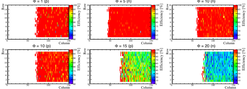
An analog injection test was performed to check the basic functionalities of the electronics after irradiation. This consists of injecting a certain number of large amplitude test pulses in each analog pixels and measure how many of these pulses are detected. In non-irradiated devices all the pulses are detected by all pixels, and the results of the scan is an uniform map of the pixel matrix as shown in figure 5(a). Since the injection is performed directly in the pre-amplifier, the effect of Non-Ionising Energy Loss (NIEL) in the silicon bulk for irradiated devices have negligible impact in this type of tests and thus only the behaviour of analog and digital electronics is investigated.
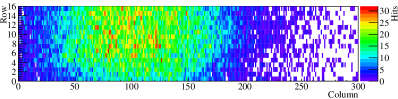
After neutron irradiation up to , the whole matrix still responds to injection, while for larger neutron fluences and for proton irradiations some pixels are unresponsive and some others respond up to five times more than expected. In neutron irradiated chips this behaviour shows up especially when chips are operated at temperatures below . This effect is observed to be in general larger after proton irradiations probably due to the significantly higher TID with respect to neutron irradiations. The largest number of mis-behaving pixel is observed after proton irradiation to the fluence of , the resulting analog injection test maps are shown in figure 6. As can be evinced from these maps, the effect cannot be associated with cross talk between pixels neither in the analog matrix (figure 6(a)) nor in the the ROC pixels of the digital periphery (figure 6(b)). In the latter it is otherwise evident that the pattern comes from a crosstalk between adjacent row address digital lines: When in the row address appears the pattern ”101”, the central bit, which is at 0, flips to 1 giving as output systematically the wrong row address. Annealing was observed to increase the number of misbehaving pixels in all irradiated devices. Also neutron irradiated chips which did not present misbehaving pixels just after irradiation, began to show this crosstalk effect after accumulating few days at room temperature due to transportation and handling. This design problem was identified and corrected for the next generations of AMS prototypes for ATLAS. Anyhow, as a workaround to still perform measurements on the H35DEMO prototype it was possible to recover the uniformity of the chip response by increasing the digital voltage (VDDD) of the chip from up to depending on the irradiation levels and types. This prevents the cross talk, but at the same time increases the noise especially in the pixels close to the digital periphery.
5 Current-Bias (I-V) characterisation
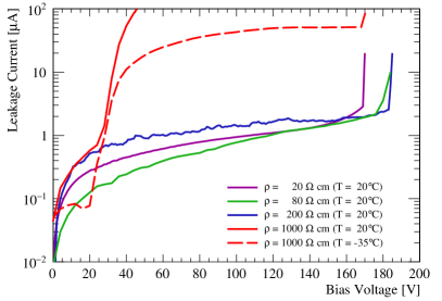
The leakage current of the p-n junction as function of applied bias (IV) was measured at stable temperature in a climate chamber. As shown in figure 7, devices with a resistivity of experience the breakdown between before irradiation and mostly above fter irradiation. A steep increase of the current around is instead observed in the sample before irradiation. This was initially mistaken for a breakdown. Instead by measuring the module at , thus reducing the leakage current below the instrument compliance to explore larger voltage biases, a second plateau is observed over . After this step the real breakdown occurs at about similarly to what observed for the other devices. This behaviour was also observed in samples used for CCPD studies [8], and was explained by the Rise-And-Flatten (RAF) effect [13]. Due to the very high leakage current, it was not possible to operate and measure this device at beam tests.
Irradiated devices show an increase of the leakage current with the fluence consistent with the linear expectation within the large uncertainties on the annealing times due to transport and handling.
6 Threshold tuning and noise
By setting dedicated internal Digital to Analog Converter (DAC) registers and applying external voltages through a DAC on the PCB, three main parameters can be tuned in the chip which have an effect on the threshold of the CMOS matrix. These are the feedback current of the in-pixel pre-amplifier (VNFBPix), the gain of the pre-amplifier (tuned by changing the voltage difference between nBLPix and ThPix) and the threshold of the discriminator in the periphery with respect to the baseline. The latter is set over the noise by changing the voltage difference between two global parameters (Th and nBL) which affect the whole matrix, and can be fine adjusted for each pixel with dedicated trim registers implemented in the chip. A trim global step register (VPTrim) allows to define the amount of adjustment obtained by moving each trim register. The trim registers are disabled in the default configuration of the left sub-matrix, but not in the right one where a correction towards larger thresholds and proportional to the value of the VPTrim global register is always applied. The tuning strategy for the presented measurements aimed at obtaining the lowest possible threshold on the left sub-matrix by changing the global parameters and subsequently rising the threshold on the right sub-matrix to minimise the noise level by increasing the VPTrim register. The fine tuning of the off-pixel trim registers of the CMOS matrix was not showing significant improvements in the threshold distribution and was therefore omitted.
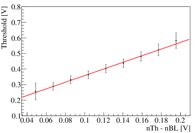
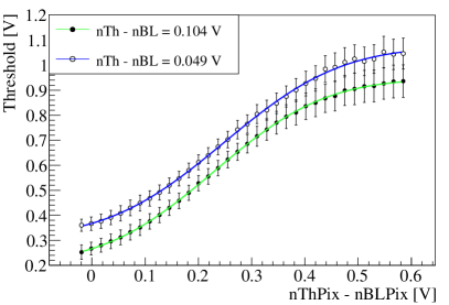
The charge injection circuit included in each pixel allows to use an external test pulse to measure the occupancy point which defines the value of the threshold. The variation of the mean threshold distribution of the pixels in the CMOS left sub-matrix as a function of the global register settings is shown in figure 8. When changing the off-pixel threshold settings a linear response is observed, while changing the global gain register the behaviour of the mean threshold distribution is well described in the measured range by an error function.
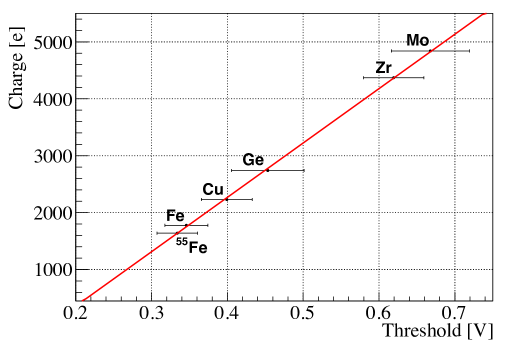
The correspondent equivalent injected charge was measured using an x-ray fluorescence setup at CERN with different target materials (Iron, Copper, Germanium, Zirconium, Molybdenum) and a radioactive source emitting gammas. The integral of the photon spectrum is obtained by measuring the average response frequency (number of hits per second) of the pixels while scanning over the threshold range. This method relies on the assumption of full charge collection from photon interaction. The result of the measurements is shown in figure 9. The calibration of the injected voltage to charge in unit of number of electrons extrapolated by a linear fit to the data is used in the following.
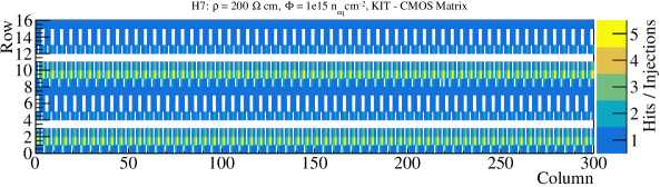
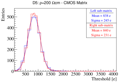
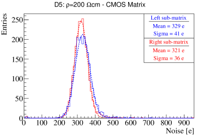
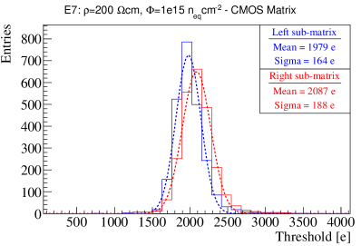
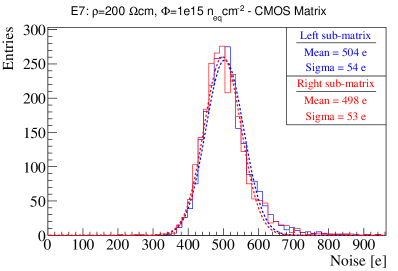
An example of threshold tuning and correspondent noise for a chip before irradiation is shown in figure 10. The module was kept at the constant temperature of inside a climate chamber. A threshold of with a sigma dispersion of about was obtained. Typical threshold noise values before irradiation are usually contained below and in the case of the tuning presented the mean noise is about with a sigma of about . After irradiation the minimum achievable threshold is usually between , depending on the irradiation dose, with a higher mean noise between but mostly contained within . An example is shown in figure 11 for a chip irradiated with neutrons to . The lowest thresholds were obtained for the left sub-matrix only.
7 Beam test campaigns: setups and analysis method
Beam test campaigns were carried out at the CERN Super Proton Synchrotron (SPS) in the H8 beam line with pions, at the MTEST facility of the Fermilab National Accelerator Laboratory (FNAL) with protons, and at Deutsches Elektronen-Synchrotron (DESY) with electrons and positrons between and . At CERN and Fermilab the UniGe FE-I4 telescope [14] was used as reference to measure the particle trajectories. It consists of six ATLAS FE-I4B planar pixel sensors from the IBL production read out with the RCE system [15]. An AIDA EUDET-type telescope [16] made of six MIMOSA26 tracking planes and an FE-I4B planar pixel sensor as time reference was instead employed at DESY. With both telescope systems the trigger-busy signals described in section 2 were used to synchronise the data with the IFAE readout system. In the case of the FE-I4 telescope the signals are handled by the RCE directly, while at DESY the AIDA TLU and the EUDAQ software are used to synchronise and merge the data of the EUDET telescope, the FE-I4B reference plane readout by a USBPix3 DAQ system [17], and the IFAE readout system.
In the FE-I4 telescope the trigger signal is given by the coincidence of hits in the first and last planes. As consequence of a trigger, hits in the telescope planes are integrated over a maximum time of , i.e. 16 LHC bunch crossings. In the IFAE readout system, instead, a time window of about is selected to save the data coming from the H35DEMO chip. This large time window is necessary given the readout architecture of the chip in order to accommodate for the full readout of the EOCs of each half matrix containing the data related to the trigger event.
In the case of the EUDET telescope instead, particles are triggered by the coincidence of four scintillators overlapping over the area of a MIMOSA sensors, two are placed in front of the upstream arm and two behind the downstream arm. Since the integration time of the MIMOSA26 is much larger than the one necessary to read out the H35DEMO, additional tracks may be reconstructed which are not associated to the main particle triggered by the scintillators. To avoid an underestimation of the efficiency, an FE-I4 pixel module which has a triggered readout with a timing precision of is used as reference. For the analysis, only tracks pointing to a correspondent hit in the FE-I4 reference plane are selected.
For the reconstruction of reference tracks and extrapolation of the impact point on the detectors under test the Proteus software [18] was used for the FE-I4 telescope data, while for the EUDET telescope data the reconstruction and analysis frameworks EUTelescope and TBmonII were used [19, 20].
A report of the very first beam test campaign at CERN SPS in 2016 can be found in ref. [21]. In this campaign the readout system was still a preliminary version showing stability problems and limitations that required a re-synchronisation of the events in the offline analysis. An upgrade of the readout system and a better understanding of the H35DEMO chip allowed to improve the integration with the FE-I4 telescope for better stability of the data taking. The results presented in this paper are obtained with this last version of the IFAE readout system.
8 Beam test results
A full characterisation at different irradiation levels of chips with a substrate resistivity of was possible due to the large availability of these devices coming from the same wafer. Just few chips of other resistivities were instead available for these studies and thus were only measured and compared before irradiation.
8.1 Operations and tunings
Non-irradiated chips produced with three different resistivities, , were mounted on standalone PCBs and the CMOS monolithic matrix was measured in the beam at Fermilab. They were operated at room temperature with active heat dissipation using a fan blowing on the back of the device. A tuning of the CMOS matrix was performed aiming at the lowest threshold. After such tuning the left and right part of the matrix resulted in different threshold distributions and are thus considered separately in the analysis. The measured mean of the threshold distributions for the different chips was measured in both parts of the CMOS matrix and are summarised in table 2.
| Device | Resistivity | Irradiation fluence | Mean threshold | Mean threshold | VDDD |
|---|---|---|---|---|---|
| name | [] (type) | left | right | ||
| UG20-1 | 20 | 0 | 1350 | 1500 | 3.3 |
| UG80-2 | 80 | 0 | 1300 | 1700 | 3.3 |
| D5 | 200 | 0 | 800 | 1100 | 3.3 |
| E5 | 200 | 5 (n) | 1700 | - | 3.3 |
| E7 | 200 | 10 (n) | 1700 | - | 3.3 |
| E10 | 200 | 1 (p) | 2100 | - | 3.9 |
| H7 | 200 | 10 (p) | 1700 | - | 4.5 |
| D6 | 200 | 15 (n) | 1700 | - | 3.9 |
| D9 | 200 | 20 (n) | 2450 | - | 4.0 |
With the sample it was possible to reach thresholds as low as . In the resistivity samples instead the tuning procedure resulted in a larger threshold of for the left part of the matrix and 1700 e for the right part of the matrix due to the noise that was found to be higher than for the chips. In the the larger noise may come from the large leakage current observed in the first version of the standalone PCB as explained in section 3, while for the chips the higher noise may be connected with the substrate resistivity.
After irradiation the chips were operated at an environmental temperatures between using a chiller based cooling box at SPS, and between with dry ice at DESY. Due to the address crosstalk problem described in section 4, chips irradiated with neutron to fluences of more than and proton irradiated chips were operated increasing VDDD as described in table 2. Moreover, the threshold optimisation and the analysis was performed only for the left sub-matrix because of difficulties in obtaining an uniform tuning at low thresholds for irradiated chips in both left and right sub-matrices.
8.2 Cluster properties
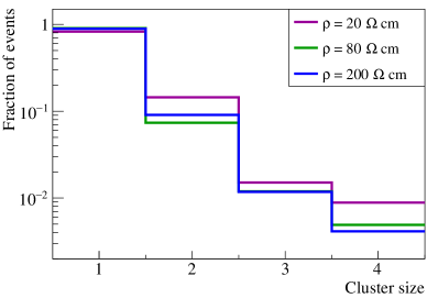
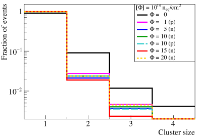
The cluster size distribution measured at beam tests for modules before and after irradiation is shown in figure 12. In these studies the beam was always impinging perpendicularly to the pixel surface, therefore a cluster size larger than one is expected only due to charge sharing out of lateral diffusion or eventually delta electrons. Before irradiation the fraction of cluster size two is about in the samples, while in the a percent of clusters size two of about is observed. This difference is anyhow marginally significant given an uncertainty of up to 2 degrees in the alignment which leads to an uncertainty in the cluster fraction estimation of about .
After irradiation events with a cluster size larger than one are reduced by a factor 8-9 with respect to events before irradiations. This is expected due to charge trapping which reduces diffusion and the higher thresholds at which the chips were operated. The effect of the threshold variation on the cluster size was measured on the chip irradiated with neutrons to and found to be less than .
8.3 Efficiency before irradiation
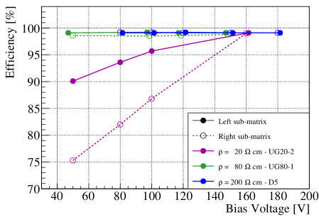
The hit efficiency measured as a function of the bias voltage is shown in figure 13(a). For resistivities of the hit efficiency is above already applying a bias voltage of , while for the sample it was necessary to bias the junction with at least to obtain the same results. This is explained with the lower depletion depth expected for such low resistivity [22, 7] which leads to a lower charge signal. Indeed, at lower voltages the hit efficiency decreases and a difference between the left and the right part of the CMOS matrix arises due to the slightly different threshold levels. This hit efficiency difference decreases as the bias voltage, and thus the signal, increases. This is the expected behaviour when the threshold is very close to the collected charge.
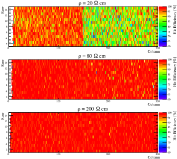
Figure 13(b) shows the hit efficiency distribution over the CMOS matrix when biased to . In the sample and faintly also in the sample, it is possible to appreciate the different efficiency between left and the right sub-matrices which is uniform within each sub-matrix. In the case of , instead, the hit efficiency is uniform over the whole pixel area.
8.4 Efficiency after irradiation
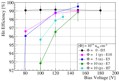
The hit efficiency measured after irradiation as function of the bias voltage for the samples is shown in figure 14. An efficiency over was obtained for all modules irradiated up to either with protons or neutrons by applying a bias voltage larger than . For larger irradiation fluences an efficiency lower than was found up to the measured voltage of which is close to the breakdown. A larger bias voltage and lower thresholds would be necessary to operate this technology at fluences larger than . In chips exposed to the same type of irradiation a correlation between the fluence and the hit efficiency is observed. A larger efficiency is instead measured in the chip irradiated with protons to with respect to the one irradiated with neutrons to the same fluence despite the higher threshold of the first one. This can be explained by the larger depletion depth which is obtained with proton irradiation with respect to neutron irradiation as observed in TCT measurements due to acceptor removal effect [22]. For almost all irradiated samples up to the same efficiency as measured before irradiation is recovered with a bias voltage of . The only exception is the H7 sensor irradiated with protons for which the measurements were limited to by the lower breakdown voltage.
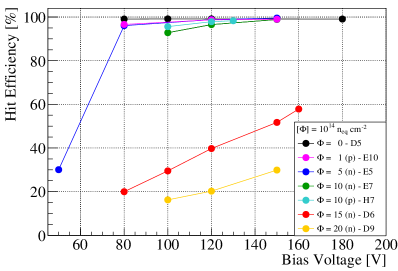
The hit efficiency over the left sub-matrix is shown in figure 15 for the highest measured voltage point. As before irradiation, the efficiency is uniform over the sub-matrix surface for all irradiation types and fluences. The expected fluctuations close to the boundary of the acceptance window of the telescope trigger are observed due to the low track statistics.
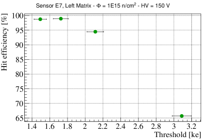
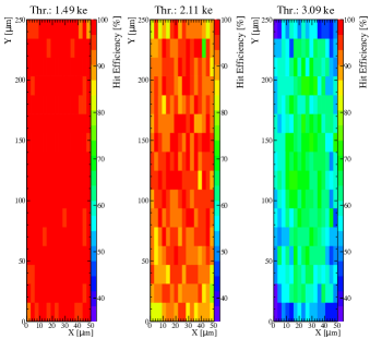
In figure 16 the efficiency of a sample irradiated with neutrons to was measured as a function of the threshold while biased to . With a threshold equal or lower than an efficiency of about was achieved. The efficiency gets just below with a threshold of about and then dramatically drops below for larger threshold values. The correspondent distribution of the hit efficiency over a pixel cell is shown in figure 16(b). When the global hit efficiency is close to , the hit efficiency is distributed uniformly over the pixel surface. As the threshold is increased inefficient regions are observed close to the boundaries of the cells and in particular in the corners between four pixels. This is due to charge sharing between neighbouring pixels which reduces the charge signal in each channel increasing the probability of falling below threshold.
From these results we can conclude that a bias voltage equal or larger than and a maximum threshold of are necessary to operate samples with an efficiency larger than up to irradiation fluences of .
9 Noise occupancy and power consumption
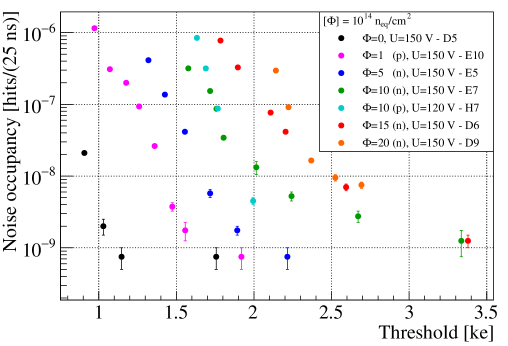
In order to fully evaluate the performance of the chip the results of the hit efficiency need to be evaluated together with the noise occupancy. For the ATLAS experiment a noise occupancy per pixel of less than hits in , i.e. a LHC bunch crossing, is required.
The noise occupancy of the left sub-matrix was measured for irradiated and non-irradiated chips in a climate chamber at stable temperatures: Non-irradiated devices were kept at , while irradiated devices were cooled down to . This is estimated to be equivalent to a temperature on chip, when configured, of approximately and , respectively. All chips were operated at the voltage for which the highest hit efficiency was measured and in the same conditions as they were operated at beam tests. An acquisition window of was used in absence of radioactive sources to integrate the noise hits. Given the small dimensions of the matrix the cosmic muon background is considered negligible.
Noise occupancy results as a function of the threshold are showed in figure 17. Before irradiation the noise occupancy in the full left sub-matrix reaches a maximum of at the lowest measured threshold of , otherwise it falls below with thresholds higher than . After irradiation the noise occupancy can be still kept below in the case of neutron irradiations even with thresholds between with which a hit efficiency of about was achieved at beam tests. This correspond to a noise occupancy per pixel of about well below the ATLAS requirements.
A power consumption of about per pixel was measured using the DAC settings with which the chips were operated at the beam test. This includes a contribution of per pixel from the digital part which is powered with , and per pixel from the analog part which is powered with . These results are consistent with the simulations published in ref. [5]. No significant variation of the power consumption of the chip was observed after irradiation apart from the need of rising the digital voltage to avoid the mentioned crosstalk effect discussed in section 4.
10 Conclusions and outlook
Very first results of the characterisation of the H35DEMO chip have been presented demonstrating the feasibility of producing large monolithic devices using a cost-effective CMOS process to fulfil the requirements in terms of radiation hardness for the ATLAS experiment at HL-LHC. The monolithic CMOS matrix of the H35DEMO was operated for minimum ionising particle detection using the DAQ system developed at IFAE. Before irradiation a comparison of the performance of different resistivities measured at beam tests showed best results for with respect to the usual resistivity substrates commonly used in the industrial CMOS process. Devices with higher resistivity substrates were able to reach a detection efficiency around with a bias voltages lower than .
After irradiation several problems have been identified in the monolithic part of this first large area prototype which need to be considered in the designs of future chips. Nevertheless, a characterisation of detection performance was possible up the radiation fluences expected for the outermost pixel layer of the ATLAS experiment at HL-LHC. The results demonstrated the radiation hardness of this large electrode design after neutron irradiation up to a fluence of showing an hit efficiency of at with an occupancy of less than noise hits in a LHC bunch crossing of . A hit efficiency of more than was also measured for proton irradiated chips with after a particle fluence of .
The performance of this technology could be taken farther by improving the tuning capabilities to reduce the threshold dispersion, and implement the possibility of effectively masking single pixels. Moreover, the performance of this chip is also limited by the H35 process which was chosen to contain the costs and eventually investigate this technology for less demanding applications in terms of radiation hardness. In particular, by moving to a CMOS process in that allows to fit more functionalities within a smaller pixel area, the radiation hardness of the digital part will be improved and at the same time the capacitance of the pixel reduced. Moreover, the power dissipation will also improve given the lower bias voltages required for the electronics in this technology with respect the H35. The H18 technology is not only available at AMS, but also in other foundries, such as TSI [23] in the United States, giving the flexibility of moving the process to another foundry in case of issues and in view of large productions.
The ATLASPix, a series of large area HV-CMOS chips has been already designed in CMOS H18 AMS technology and the first prototype, the ATLASPix1, has been already produced and successfully tested before irradiation [24]. The ATLASPix2 has been also submitted for production at TSI in June 2018. This new generation of monolithic prototypes for ATLAS aims at moving towards a final demonstrator by consolidating the radiation hardness features of this design and including all the functionalities required by the ATLAS experiment. In particular it will have to investigate the possibility of matching the requirements in terms of timing and in-time efficiency which were not met by previous prototypes as shown by the measurements preformed on CCPDs [4, 8].
Acknowledgments
This work was partially funded by: the Generalitat de Catalunya (AGAUR 2014 SGR 1177), the MINECO, Spanish Government, under grants FPA2015-69260-C3-2-R, FPA2015-69260-C3-3-R (co-financed with the European Union’s FEDER funds) and SEV-2012-0234 (Severo Ochoa excellence programme), under the Juan de la Cierva programme; the European Union’s Horizon 2020 Research and Innovation programme under Grant Agreement no. 654168; and the PhD fellowship program of La Obra Social La Caixa-Severo Ochoa. The authors would like to thank A. Dierlamm and F. Bögelspacher (KIT) as well as V. Cindro and I. Mandic (JSI) for the excellent support for the irradiations, and S. Kühn and S. Dungs for the availability and support with the x-ray fluorescence setup at CERN.
References
- [1] I. Perić et al., A novel monolithic pixelated particle detector implemented in high-voltage CMOS technology, Nucl. Instrum. Meth. A 582 (2007) 876.
- [2] ATLAS Collaboration, ATLAS Insertable B-Layer Technical Design Report, Tech. Rep. CERN-LHCC-2010-013, ATLAS-TDR-19, CERN, September 2010, [https://cds.cern.ch/record/1291633].
- [3] AMS AG, Austria Mikro Systeme, [http://ams.com].
- [4] M. Benoit et al., Testbeam results of irradiated ams H18 HV-CMOS pixel sensor prototypes, JINST 13 (2018), P02011.
- [5] E. Vilella et al., Prototyping of an HV-CMOS demonstrator for the High Luminosity-LHC upgrade, JINST 11 (2016) no. 1, C01012.
- [6] M. Garcia-Sciveres et al., The FE-I4 pixel readout integrated circuit, Nucl. Instrum. Meth. A 636 (2011) S155.
- [7] E. Cavallaro et al., Studies of irradiated AMS H35 CMOS detectors for the ATLAS tracker upgrade, JINST 12 (2017) no. 1, C01074.
- [8] M. Benoit et al., Test beam measurement of ams H35 HV-CMOS capacitively coupled pixel sensor prototypes with high-resistivity substrate, JINST 13 (2018) no.12, P12009.
- [9] R. Casanova et al., Design and characterization of the monolithic matrices of the H35DEMO chip, PoS TWEPP-17 (2018) 029.
- [10] Irradiation Center at the Karlsruhe Institute of Technology (KIT), [http://www.etp.kit.edu/english/irradiation_center.php].
- [11] The Reactor Center Podgorica of the Jožef Stefan Institute, [http://www.rcp.ijs.si].
- [12] I. Mandić et al., Bulk Damage in DMILL npn Bipolar Transistors Caused by Thermal Neutrons Versus Protons and Fast Neutrons, IEEE Transaction on Nuclear Science 51 (2004) no. 4.
- [13] D M S Sultan et. al., Characterization of the first double-sided 3D radiation sensors fabricated at FBK on 6-inch silicon wafers, JINST (2015), no. 10, C12009.
- [14] M. Benoit et al., The FE-I4 telescope for particle tracking in testbeam experiments, JINST 11 (2016) P07003.
- [15] R. Herbst et al., Design of the SLAC RCE Platform: A general purpose ATCA based data acquisition system, in Proceedings of RTSD 2014, Seattle, WA, USA, November 8-15, 2014.
- [16] I. Rubinskiy et al., An EUDET/AIDA Pixel Beam Telescope for Detector Development, Phys. Proc. 37 (2012) 923.
- [17] V. Filimonov et al., A serial powering pixel stave prototype for the ATLAS ITk upgrade, JINST 12 (2017) no. 03, C03045.
- [18] M. Kiehn et al., Proteus pixel telescope reconstruction, [https://gitlab.cern.ch/unige-fei4tel/proteus].
- [19] EUTelescope - A Generic Pixel Telescope Data Analysis Framework, [http://eutelescope.web.cern.ch].
- [20] TBmonII Test Beam Analysis Framework, [https://bitbucket.org/TBmon2/tbmon2/overview].
- [21] S. Terzo et al., Characterisation of novel prototypes of monolithic HV-CMOS pixel detectors for high energy physics experiments, JINST 12 (2017) no. 06, C06009.
- [22] J. Anders et al., Charge collection characterisation with the Transient Current Technique of the ams H35DEMO CMOS detector after proton irradiation, JINST 13 (2018), P10004.
- [23] TSI Semiconductors Corp., [http://www.tsisemi.com].
- [24] M. Kiehn et al., Performance of CMOS pixel sensor prototypes in ams H35 and aH18 technology for the ATLAS ITk upgrade, Nucl. Instrum. Meth. A (2018) In Press.