Highly anisotropic thermoelectric properties of carbon sulfide monolayers
Abstract
Strain engineering applied to carbon monosulphide monolayers allows to control the bandgap, controlling electronic and thermoelectric responses. Herein, we study the semiconductor-metal phase transition of this layered material driven by strain control on the basis of first-principles calculations. We consider uniaxial and biaxial tensile strain and we find a highly anisotropic electronic and thermoelectonic responses depending on the direction of the applied strain. Our results indicate that strain-induced response could be an effective method to control the electronic response and the thermoelectric performance.
I Introduction
In recent years new phenomena emerging from two-dimensional materials have been explored. Despite the exciting new electronic properties that make it possible to design new applicationsJariwala et al. (2014); Fiori et al. (2014), one of the biggest challenges ahead is to control bandgap in a systematic way. Several solutions are currently being considered such as dopingMahmood et al. (2015); González et al. (2015), stacking ordersDai and Zeng (2014); Cortés et al. (2018); Chico et al. (2017); González et al. (2010) or strainFrisenda et al. (2017); Zhang et al. (2014). Research into two-dimensional (2D) materials goes beyond grapheneBhimanapati et al. (2015); Das et al. (2015). On one hand, elements of the same carbon group have been considered to produce layered materials, for instance the silicene, germanene or stanene monolayersBalendhran et al. (2015); Lalmi et al. (2010). On the other hand, the quest for new electronic properties in layered materials has been extended to the various phosphorus-based assembles, in particular the black phosphorus monolayers or phosphorene may impact on future technologiesLi et al. (2014). Following these trends, our goal is to demonstrate the interesting properties of the recently predicted carbon sulfide monolayer (CS monolayer) which is isoelectronic to phosphoreneAlonso-Lanza et al. (2017) and its possible control under external strain.
In two-dimensional systems, strain can be applied indirectly by using thermal variations of the substrateFrisenda et al. (2017) or directly by mechanical deformationsLee et al. (2012); Caneva et al. (2018). Theoretical studies predict that most 2D materials can tolerate strain values above 10% without rupturesFrisenda et al. (2017); Bertolazzi et al. (2011); Caneva et al. (2018). For example, the graphene monolayers can easily tolerate strain above 25%Lee et al. (2008). Our aim is to provide a general picture of the connection between electronic and thermoelectronic properties upon external strain, highlighting the efficiency of the strain applied in certain directions to control the bandgap.
Herein, we employ first-principles calculations to study the electronic and thermoelectronic response upon strain for the carbon sulfide monolayers. Calculations show that the CS monolayer is a semiconductor stable at room temperature with an indirect bandgapAlonso-Lanza et al. (2017). Its structure is composed by single layer with two-dimensional honeycomb puckered structure where each atom is bonded to three neighbors. Because the CS monolayer has a structure similar to phosphorene, therefore we anticipate a similar improvement in mechanical flexibilityWei and Peng (2014) and highly anisotropic electronic propertiesLi et al. (2014).
II Methodology
Density functional theory calculations were performed using the plane-wave self-consistent field plane-wave implemented in the Quantum ESPRESSO packageGiannozzi et al. (2009) with the generalized gradient approximation of Perdew-Burke-Ernzerhof (PBE) exchange-correlation functionalPerdew et al. (1996); pse . Self-consistent charge calculations are converged up to a tolerance of for the unit cell. Monolayers are repeated periodically separated by 20 Å of empty space in the perpendicular direction. A fine k-grid of Monkhorst-Pack is used to sample the Brillouin zone and the orbitals were expanded in plane waves until a kinetic energy cutoff of eV. All atoms are allowed to relax within the conjugate gradient method until forces have been converged with a tolerance of eV/Å. For the calculation of the transport coefficients a denser k-grid of Monkhorst-Pack is used to sample the Brillouin zone.
In general, an accurate description of the bandgap requires sophisticated semi-local exchange-correlation approaches as the GW approximationTran and Blaha (2009); Tran et al. (2014). However, under experimental conditions, samples are subject to external factors such as doping or interaction with substrates. Therefore, the electronic screening is significantly weaker than in the isolated case and as a consequence the bandgap tends to be smallerHybertsen and Louie (1986). In order to consider the external factors, we calculate the thermoelectric coefficients using PBE-DFT band structure, that can be used as a lower limit of the bandgapFei et al. (2014).
The electronic transport coefficients are derived from the electronic band structure based on the semiclassical Boltzmann transport theory within the constant relaxation time approximation (RTA), as implemented in the BoltzTraP codeMadsen and Singh (2006). In this approximation, the relaxation time is a constant and therefore the thermopower or Seebeck coefficient is independent of the relaxation time. The constant relaxation time approximation has been successfully used to describe the transport coefficients of a wide range of thermoelectric materials Li et al. (2016); Hung et al. (2015); Yang et al. (2014); Peng et al. (2011).
The Seebeck coefficient at the temperature and chemical potential can be expressed asMadsen and Singh (2006); Scheidemantel et al. (2003),
| (1) |
being the scalar conductivity defined by
| (2) |
with the transport distribution defined as
| (3) |
where is the carrier charge, the Fermi distribution, the Boltzmann constant, the constant relaxation time and the group velocity of the state labeled with .
III Results and Discussion
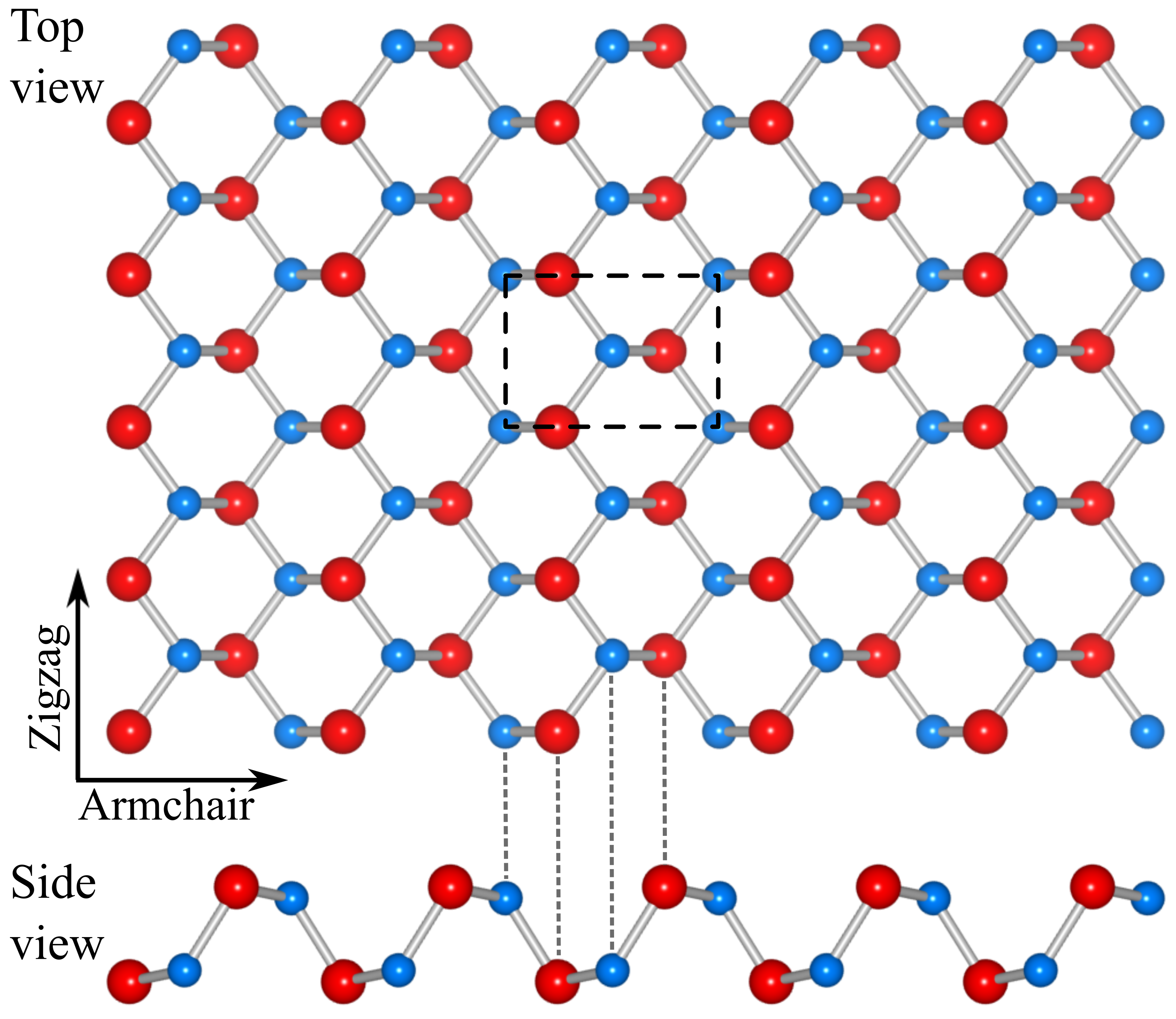
Figure 1 shows the most stable CS monolayer structure, corresponding to a hexagonal structure with puckered sheets of bounded atoms in the same way as phosporene. Similar structures can be found in group IV monochalcogenides (for instance GeSe, GeS, SnSe, SnS)Singh and Hennig (2014); Hu et al. (2015); Vaughn et al. (2010), and group V semiconductors (PN or AsN)Zhu et al. (2015); Zhang et al. (2016a); Zhao et al. (2017). Each sulfur atom on the CS monolayer is bonded to three carbon atoms and vice versaAlonso-Lanza et al. (2017). An out-plane bond of length 1.84 Å and two in-plane bonds of length 1.75 Å are observed. The angles between the bonds are 102 and 105. With the optimized parameters, the relaxed in-plane lattice vectors are Å and Å.
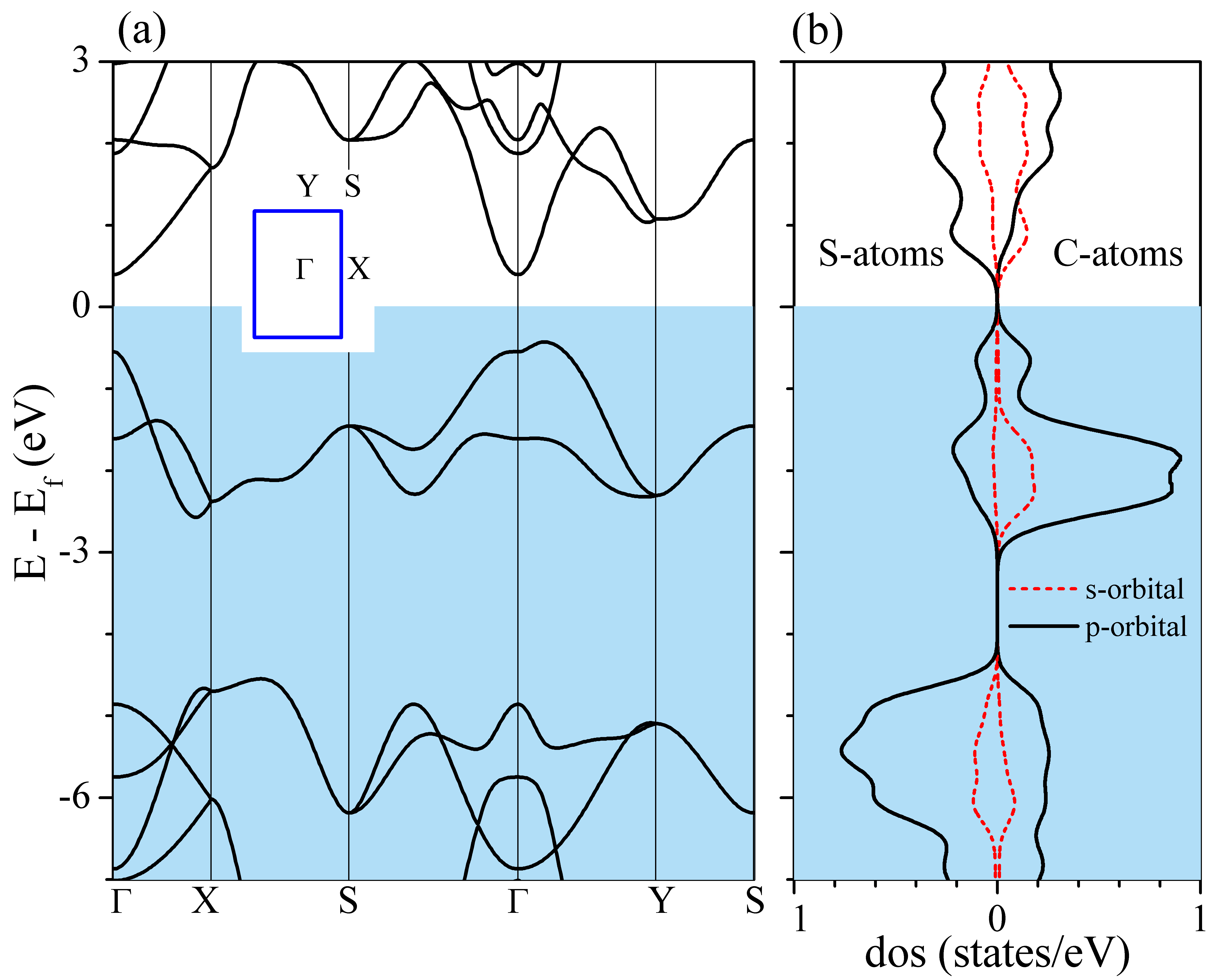
The band structure of the carbon sulfide layer in fig. 2 reveals a semiconductor with an indirect bandgap of eV, in agreement with the previous worksAlonso-Lanza et al. (2017). Slightly higher than the eV bandgap found for phosphoreneFukuoka et al. (2015); Zhang et al. (2016b); Fei et al. (2014). The occupied bands below the Fermi level have a dominant contribution of -orbitals from carbon atoms. Underneath these bands, a particular feature of the CS monolayer is the second bandgap located eV below the Fermi level. Followed by bands composed by -orbitals from sulfur atoms.
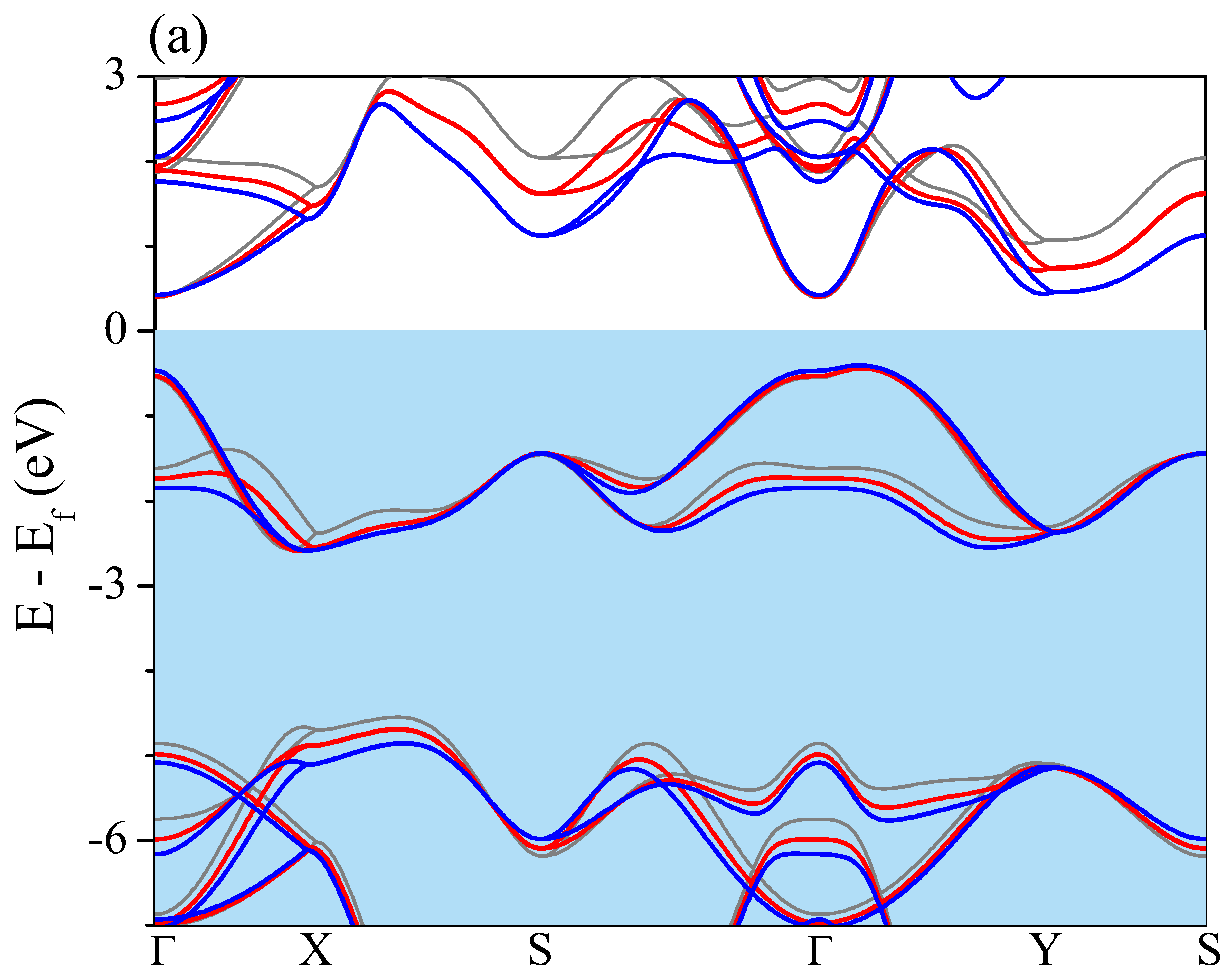
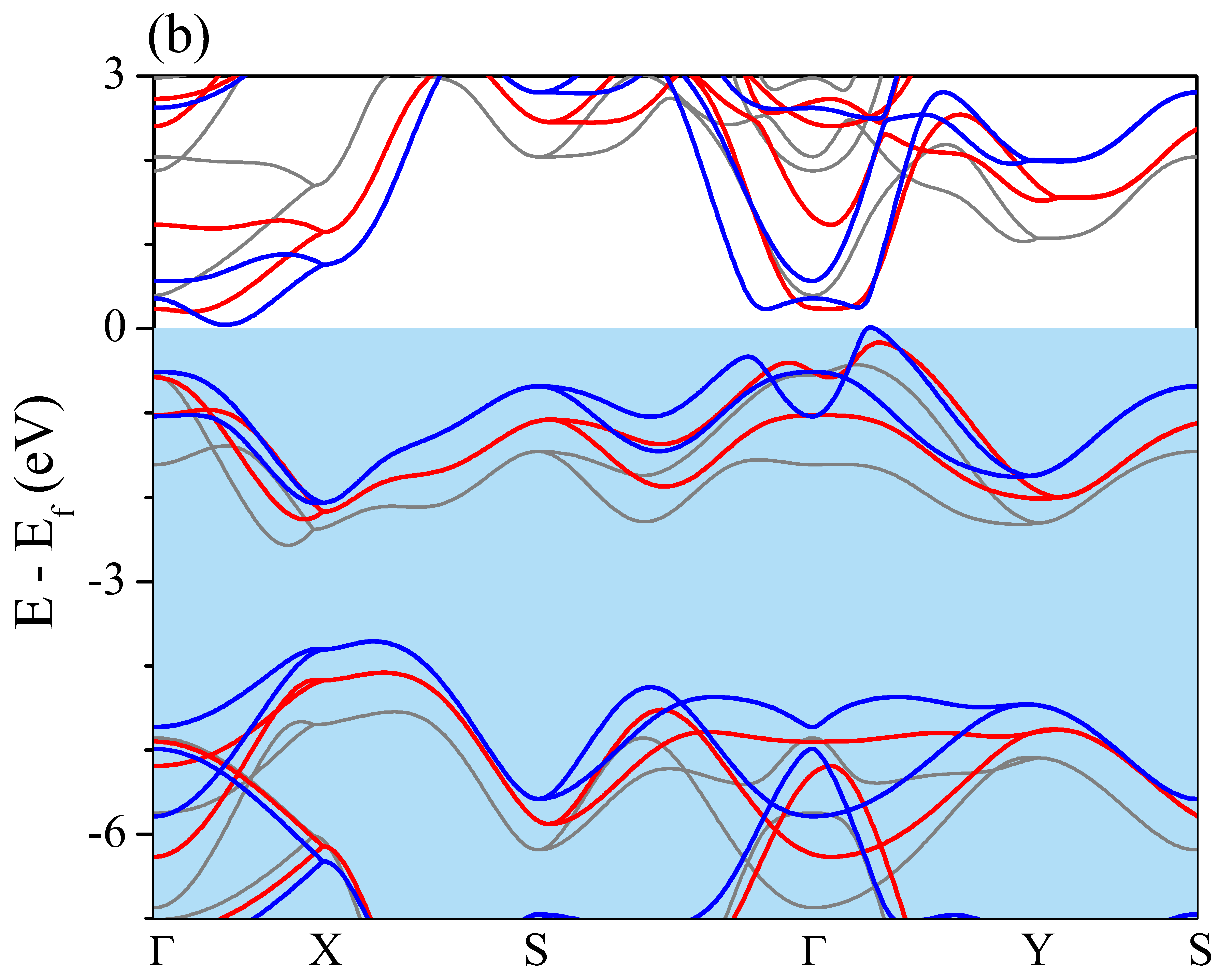
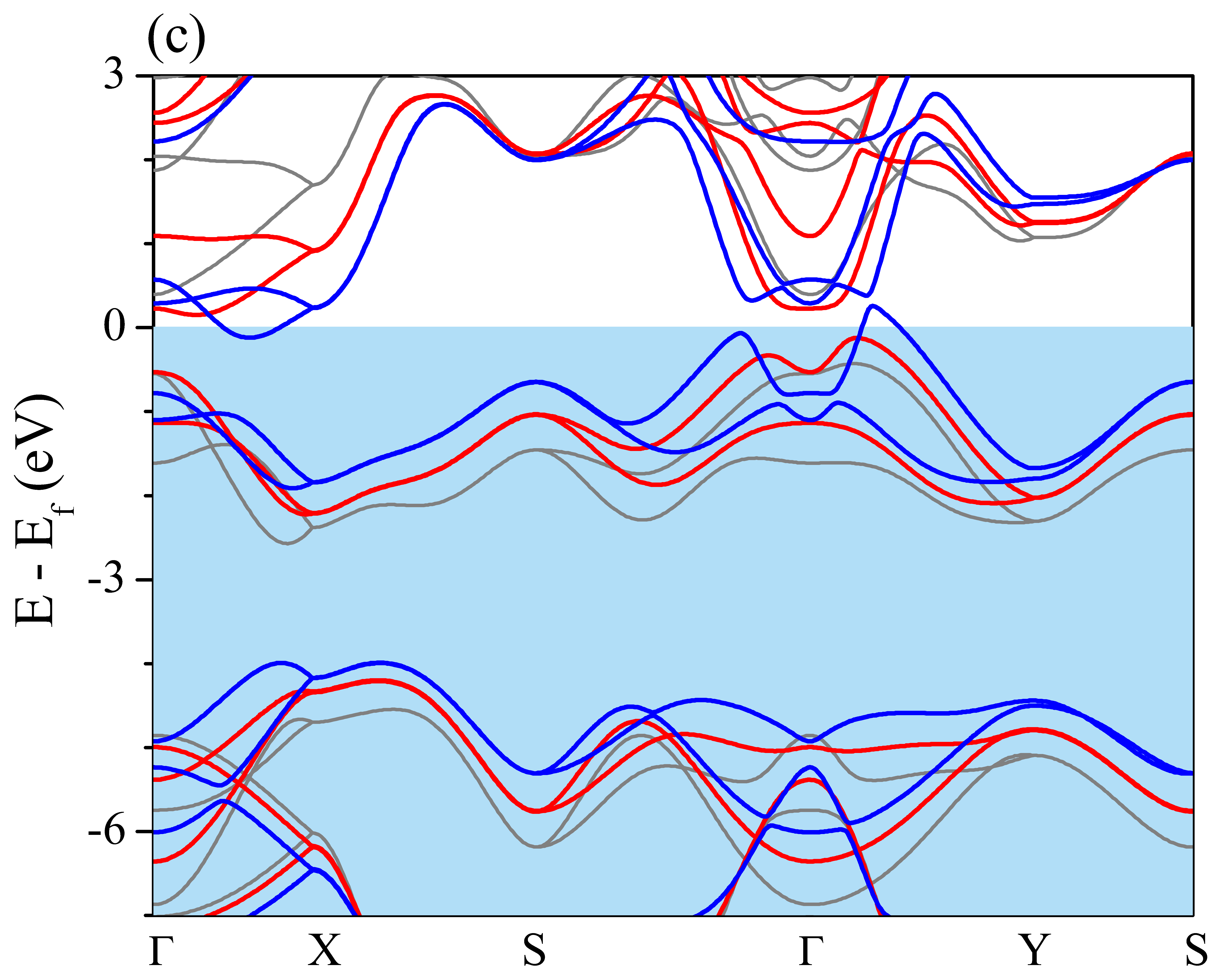
We consider two uniaxial strain cases corresponding to modifications of the unit cell in the armchair and zigzag directions, and a biaxial case corresponding to a combination of tensile strain in both armchair and zigzag directions. The strain is introduced by changing the size of the lattice vector in the selected directions and then the structure is fully relaxed. Similar to molybdenite (MoS2)Scalise et al. (2012), we find that the bandgap of the the CS monolayer decreases as the tensile strain increases. This tendency is the opposite to that observed in graphene and phosporene layersSi et al. (2016); Nguyen et al. (2015); Lv et al. (2014).
For uniaxial strain along the armchair-direction (parallel to x-axis) in fig. 3 (a), the band structure is modified marginally. As the uniaxial tension in armchair-direction increases, the bottom of the conduction band at the high symmetry -point of moves down and for a strain of 10% reaches the same level of the -point. The bandgap of the CS monolayer is more sensitive to the uniaxial strain applied along the zigzag-direction (parallel to y-axis) as shown in fig. 3 (b). Contrary to the previous case, the gap closes even for small values of strain and the bottom (top) of the conduction (valence) band moves away from the high-symmetry points. In the fig. 3 (c), we can observe that the band structure upon biaxial strain (x and y direction simultaneously) shows a behavior similar to the uniaxial case applying strain in the zigzag direction. As the strain increases, the carbon -bands move upward in energy producing several anticrossings near the Fermi level. For strain values of 10%, the HOMO-LUMO gap has completely disappeared and the transition between semiconductor and metal is complete. Note that, the second gap remains practically constant due to the almost rigid movement of the sulfur -bands.
Employing the calculated electronic band structure as input, the transport coefficients are calculate using the Boltzmann transport theory within the constant relaxation time approximation. It is possible to correlate features from band structure with some aspects shown by the Seebeck coefficient . Because electrons and holes contribute to the transport properties, the maximum of the Seebeck coefficient appears in the band gapMahan (1989); Gibbs et al. (2015) and therefore it can be controlled with strain engineering.
In our calculations the maximum Seebeck coefficient around the Fermi level at room temperature ( K) for the non-strained CS monolayer is mV/K. Under the same conditions, for the phosphorene layer we find a mV/K, in agreement with previous DFT-PBE calculationsFei et al. (2014). Note that hereafter we refer to as maximum Seebeck coefficient around the Fermi level. A second peak also appears in the Seebeck coefficient of the CS monolayer due to the second gap. We will not discuss it, because under normal experimental conditions it would be difficult to reach the level of doping necessary to be measured.
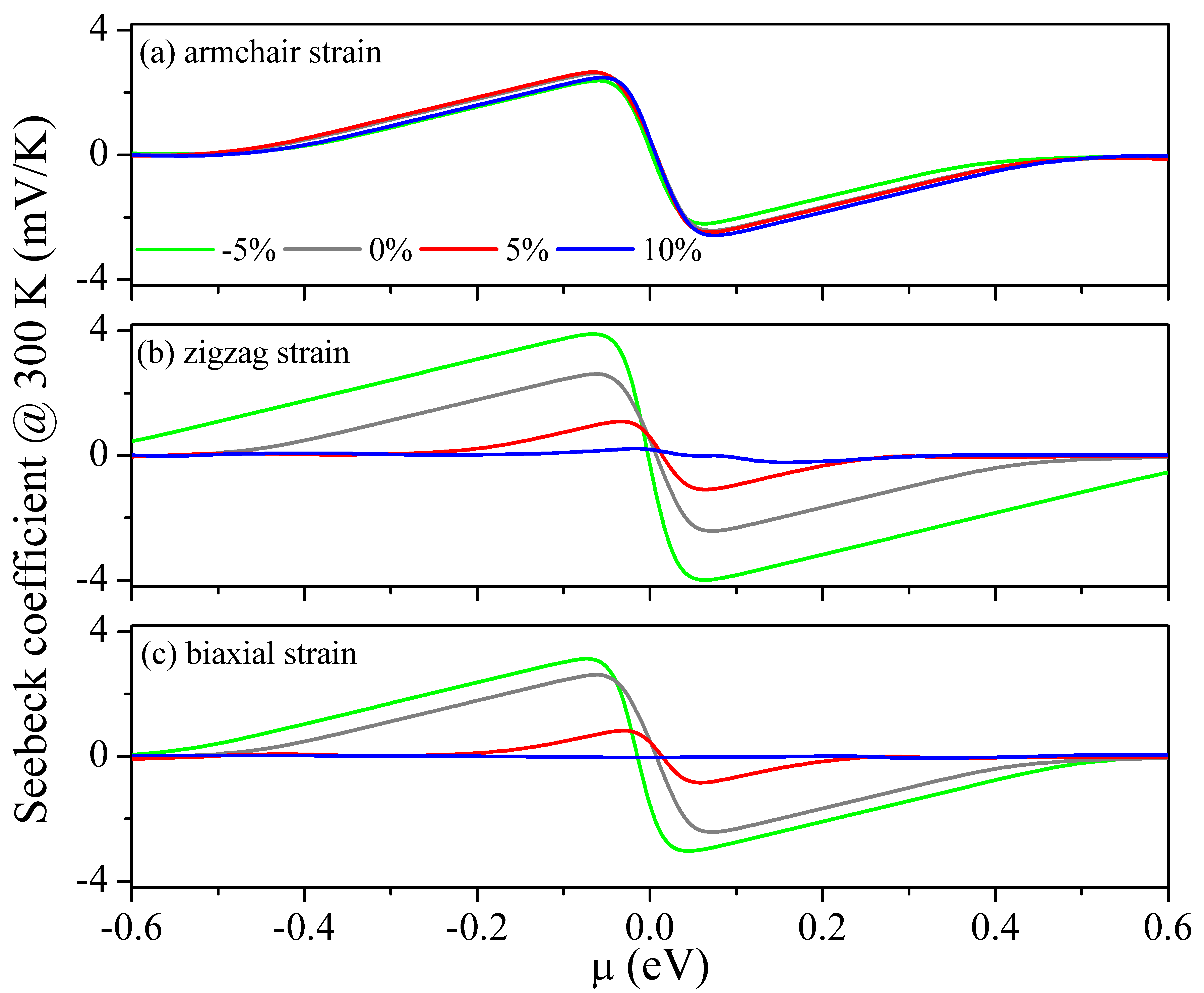
In fig. 4, we present the room temperature Seebeck coefficient of the CS monolayer as a function of chemical potential. The Seebeck coefficient is strongly modified by the chemical potential, showing that an optimal carrier concentration is crucial for efficient thermoelectric performanceFei et al. (2014). The change in the Seebeck coefficient due to the applied strain along the armchair-direction is minor, fig. 4 (a). This result can be expected from the small variations observed in the band structure upon uniaxial strain along that direction in fig. 3 (a).
Transport coefficients are easily controlled by strain in the zigzag direction. In fig. 4 (b) we can note how the behavior of the Seebeck coefficient against the chemical potential tends to a constant as the strain increases. For negative strain values corresponding to a compression of the system, we observe a large increase in the maximum value of the Seebeck coefficient. Both behaviors can be explained by the variation of the gap with the strainZhang et al. (2014).
Given the response of the band structure to strain, the behavior of the Seebeck coefficient in case of biaxial strain is similar to that of the previous case. In fig. 4 (c), for positive strain values, the Seebeck coefficient follows the same trends of the uniaxial in zigzag-direction but with slightly lower values. The difference between both cases appears when considering the structural compression, the response of the Seebeck coefficient is smaller in the biaxial case.
The maximum Seebeck coefficient decays exponentially with the temperature without modifying the behavior described above. It is possible to follow the behavior of the maximum Seebeck coefficient value for a given temperature. On the one hand, the biaxial case is more susceptible to modifications to the positive strain values (corresponding to an expansion) where rapidly tends to zero, the strain in the zigzag direction follows the same trends, and the strain in the armchair direction only produces marginal effects in . On the other hand, when considering negative strain values (corresponding to a compression) in the zigzag direction at room temperature and -5% strain the increases to mV/K, the biaxial strain case produces a slight increase of to mV/K, and contrary to these two, the strain in armchair direction produces a reduction of to mV/K. As a reference, at K for the non-strained case we find a mV/K.
As previously noted, the electronic and thermoelectronic responses of the CS monolayer are contrary to that observed in graphene and phosporene layersNguyen et al. (2015); Lv et al. (2014). Taking advantage of the fact that the Seebeck coefficient is low for conductors and the electronic conductance tends to be low for insulatorsChico et al. (2017). Devices could be designed taking advantage of inhomogeneous response upon strain using heterojunctions or controlled stacking to obtain a strain-dependent thermal and electronic responsesLado et al. (2013); Shim et al. (2016); Rosales and González (2013); Dai and Zeng (2014); González et al. (2010); Deng et al. (2014).
IV Final Remarks
In conclusion, we have investigated the strain response on the electronic and thermoelectric properties of carbon sulfide monolayer based on the PBE-DFT calculations combined with the semiclassical Boltzmann theory. We found a highly anisotropic electronic and thermoelectonic response upon strain. When the strain is applied in the armchair direction, the bandgap and Seebeck coefficient remain almost unchanged. In contrast, when strain is applied in the zigzag direction the Seebeck coefficient is easily modulated, going from a finite value to zero with relatively small strain values. By tracking the evolution of the Seebeck coefficient as a function of external strain we can follow the change in bandgap induced by the strain. Our results suggest possible applications as sensors or active component taking advantage of the real-time bandgap modulation.
Acknowledgements
The author gratefully acknowledges the critical reading of the manuscript and the suggestions made by L. Chico and S. Sadewasser.
References
- Jariwala et al. (2014) D. Jariwala, V. K. Sangwan, L. J. Lauhon, T. J. Marks, and M. C. Hersam, ACS Nano 8, 1102 (2014).
- Fiori et al. (2014) G. Fiori, F. Bonaccorso, G. Iannaccone, T. Palacios, D. Neumaier, A. Seabaugh, S. K. Banerjee, and L. Colombo, Nature Nanotechnology 9, 768 (2014).
- Mahmood et al. (2015) J. Mahmood, E. K. Lee, M. Jung, D. Shin, I.-Y. Jeon, S.-M. Jung, H.-J. Choi, J.-M. Seo, S.-Y. Bae, S.-D. Sohn, et al., Nature Communications 6, 6486 (2015).
- González et al. (2015) J. W. González, L. Rosales, M. Pacheco, and A. Ayuela, Physical Chemistry Chemical Physics 17, 24707 (2015).
- Dai and Zeng (2014) J. Dai and X. C. Zeng, J. Phys. Chem. Lett. 5, 1289 (2014).
- Cortés et al. (2018) N. Cortés, L. Rosales, P. A. Orellana, A. Ayuela, and J. W. González, Scientific Reports 8, 2143 (2018).
- Chico et al. (2017) L. Chico, P. Orellana, L. Rosales, and M. Pacheco, Physical Review Applied 8, 054029 (2017).
- González et al. (2010) J. W. González, H. Santos, M. Pacheco, L. Chico, and L. Brey, Physical Review B 81, 195406 (2010).
- Frisenda et al. (2017) R. Frisenda, R. Schmidt, S. M. de Vasconcellos, R. Bratschitsch, D. P. de Lara, and A. Castellanos-Gomez, in Optical Sensing, Imaging, and Photon Counting: Nanostructured Devices and Applications 2017 (International Society for Optics and Photonics, 2017), p. 10353.
- Zhang et al. (2014) J. Zhang, H. Liu, L. Cheng, J. Wei, J. Liang, D. Fan, J. Shi, X. Tang, and Q. Zhang, Scientific Reports 4, 6452 (2014).
- Bhimanapati et al. (2015) G. R. Bhimanapati, Z. Lin, V. Meunier, Y. Jung, J. Cha, S. Das, D. Xiao, Y. Son, M. S. Strano, V. R. Cooper, et al., ACS Nano 9, 11509 (2015).
- Das et al. (2015) S. Das, J. A. Robinson, M. Dubey, H. Terrones, and M. Terrones, Annual Review of Materials Research 45, 1 (2015).
- Balendhran et al. (2015) S. Balendhran, S. Walia, H. Nili, S. Sriram, and M. Bhaskaran, Small 11, 640 (2015).
- Lalmi et al. (2010) B. Lalmi, H. Oughaddou, H. Enriquez, A. Kara, S. Vizzini, B. Ealet, and B. Aufray, Applied Physics Letters 97, 223109 (2010).
- Li et al. (2014) L. Li, Y. Yu, G. J. Ye, Q. Ge, X. Ou, H. Wu, D. Feng, X. H. Chen, and Y. Zhang, Nature Nanotechnology 9, 372 (2014).
- Alonso-Lanza et al. (2017) T. Alonso-Lanza, F. Aguilera-Granja, J. W. González, and A. Ayuela, Physical Review Materials 1, 024001 (2017).
- Lee et al. (2012) J. E. Lee, G. Ahn, J. Shim, Y. S. Lee, and S. Ryu, Nature Communications 3, 1024 (2012).
- Caneva et al. (2018) S. Caneva, P. Gehring, V. M. García-Suárez, A. García-Fuente, D. Stefani, I. J. Olavarria-Contreras, J. Ferrer, C. Dekker, and H. S. J. van der Zant, Nature Nanotechnology (2018).
- Bertolazzi et al. (2011) S. Bertolazzi, J. Brivio, and A. Kis, ACS Nano 5, 9703 (2011).
- Lee et al. (2008) C. Lee, X. Wei, J. W. Kysar, and J. Hone, Science 321, 385 (2008).
- Wei and Peng (2014) Q. Wei and X. Peng, Applied Physics Letters 104, 251915 (2014).
- Giannozzi et al. (2009) P. Giannozzi, S. Baroni, N. Bonini, M. Calandra, R. Car, C. Cavazzoni, D. Ceresoli, G. L. Chiarotti, M. Cococcioni, I. Dabo, et al., Journal of Physics: Condensed Matter 21, 395502 (2009).
- Perdew et al. (1996) J. P. Perdew, K. Burke, and M. Ernzerhof, Physical Review Letters 77, 3865 (1996).
- (24) For carbon, sulfur and phosphorus we use the pseudopotentials C.pbe-n-kjpaw_psl.0.1.UPF, S.pbe-n-kjpaw_psl.0.1.UPF and P.pbe-n-kjpaw_psl.0.1.UPF from the Quantum ESPRESSO pseudopotential data base: http://www.quantum-espresso.org/pseudopotentials.
- Tran and Blaha (2009) F. Tran and P. Blaha, Physical Review Letters 102, 226401 (2009).
- Tran et al. (2014) V. Tran, R. Soklaski, Y. Liang, and L. Yang, Physical Review B 89, 235319 (2014).
- Hybertsen and Louie (1986) M. S. Hybertsen and S. G. Louie, Physical Review B 34, 5390 (1986).
- Fei et al. (2014) R. Fei, A. Faghaninia, R. Soklaski, J.-A. Yan, C. Lo, and L. Yang, Nano Letters 14, 6393 (2014).
- Madsen and Singh (2006) G. K. Madsen and D. J. Singh, Computer Physics Communications 175, 67 (2006).
- Li et al. (2016) Y. Li, Y. Ding, B. Xiao, and Y. Cheng, Physics Letters A 380, 3748 (2016).
- Hung et al. (2015) N. T. Hung, A. R. Nugraha, E. H. Hasdeo, M. S. Dresselhaus, and R. Saito, Physical Review B 92, 165426 (2015).
- Yang et al. (2014) G. Yang, J. Yang, Y. Yan, and Y. Wang, Physical Chemistry Chemical Physics 16, 5661 (2014).
- Peng et al. (2011) H. Peng, J.-H. Song, M. Kanatzidis, and A. J. Freeman, Physical Review B 84, 125207 (2011).
- Scheidemantel et al. (2003) T. Scheidemantel, C. Ambrosch-Draxl, T. Thonhauser, J. Badding, and J. Sofo, Physical Review B 68, 125210 (2003).
- Singh and Hennig (2014) A. K. Singh and R. G. Hennig, Applied Physics Letters 105, 042103 (2014).
- Hu et al. (2015) Y. Hu, S. Zhang, S. Sun, M. Xie, B. Cai, and H. Zeng, Applied Physics Letters 107, 122107 (2015).
- Vaughn et al. (2010) D. D. Vaughn, R. J. Patel, M. A. Hickner, and R. E. Schaak, Journal of the American Chemical Society 132, 15170 (2010).
- Zhu et al. (2015) Z. Zhu, J. Guan, D. Liu, and D. Tománek, ACS Nano 9, 8284 (2015).
- Zhang et al. (2016a) L.-C. Zhang, G. Qin, W.-Z. Fang, H.-J. Cui, Q.-R. Zheng, Q.-B. Yan, and G. Su, Scientific Reports 6 (2016a).
- Zhao et al. (2017) L. Zhao, W. Yi, J. Botana, F. Gu, and M. Miao, The Journal of Physical Chemistry C 121, 28520 (2017).
- Fukuoka et al. (2015) S. Fukuoka, T. Taen, and T. Osada, Journal of the Physical Society of Japan 84, 121004 (2015).
- Zhang et al. (2016b) R. Zhang, X. Wu, and J. Yang, Nanoscale 8, 4001 (2016b).
- Scalise et al. (2012) E. Scalise, M. Houssa, G. Pourtois, V. Afanas’ev, and A. Stesmans, Nano Research 5, 43 (2012).
- Si et al. (2016) C. Si, Z. Sun, and F. Liu, Nanoscale 8, 3207 (2016).
- Nguyen et al. (2015) M. C. Nguyen, V. H. Nguyen, H.-V. Nguyen, J. Saint-Martin, and P. Dollfus, Physica E: Low-dimensional Systems and Nanostructures 73, 207 (2015).
- Lv et al. (2014) H. Lv, W. Lu, D. Shao, and Y. Sun, Physical Review B 90, 085433 (2014).
- Mahan (1989) G. Mahan, Journal of Applied Physics 65, 1578 (1989).
- Gibbs et al. (2015) Z. M. Gibbs, H.-S. Kim, H. Wang, and G. J. Snyder, Applied Physics Letters 106, 022112 (2015).
- Lado et al. (2013) J. L. Lado, J. W. González, and J. Fernández-Rossier, Physical Review B 88, 035448 (2013).
- Shim et al. (2016) J. Shim, S. Oh, D.-H. Kang, S.-H. Jo, M. H. Ali, W.-Y. Choi, K. Heo, J. Jeon, S. Lee, M. Kim, et al., Nature Communications 7, 13413 (2016).
- Rosales and González (2013) L. Rosales and J. W. González, Nanoscale Research Letters 8, 1 (2013).
- Deng et al. (2014) Y. Deng, Z. Luo, N. J. Conrad, H. Liu, Y. Gong, S. Najmaei, P. M. Ajayan, J. Lou, X. Xu, and P. D. Ye, ACS Nano 8, 8292 (2014).