Reconfigurable edge-state engineering in graphene using LaAlO3/SrTiO3 nanostructures
Abstract
The properties of graphene depend sensitively on doping with respect to the charge-neutrality point (CNP). Tuning the CNP usually requires electrical gating or chemical doping. Here, we describe a technique to reversibly control the CNP in graphene with nanoscale precision, utilizing LaAlO3/SrTiO3 (LAO/STO) heterostructures and conductive atomic force microscope (c-AFM) lithography. The local electron density and resulting conductivity of the LAO/STO interface can be patterned with a conductive AFM tip Cen et al. (2008) , and placed within two nanometers of an active graphene device Huang et al. (2015) . The proximal LAO/STO nanostructures shift the position of graphene CNP by cm-2, and are also gateable. Here we use this effect to create reconfigurable edge states in graphene, which are probed using the quantum Hall effect. Quantized resistance plateaus at and are observed in a split Hall device, demonstrating edge transport along the c-AFM written edge that depends on the polarity of both the magnetic field and direction of currents. This technique can be readily extended to other device geometries.
Graphene has proved to be a powerful and versatile platform for studying condensed matter phenomena due to the unique honeycomb crystal structure and Dirac fermion behavior of electrons. The unique Dirac cone band structure makes it possible to tune the carrier density continuously between electrons and holes. This duality of carriers in graphene results in many exotic properties of graphene, such as Klein tunnelingAllain and Fuchs (2011); Katsnelson, Novoselov, and Geim (2006); Young and Kim (2009); Shytov, Rudner, and Levitov (2008), edge state mixingWilliams, DiCarlo, and Marcus (2007); Abanin and Levitov (2007); Lohmann, von Klitzing, and Smet (2009); Amet et al. (2014), and recently the “wedding cake” structure of quantum Hall statesGutiérrez et al. (2018). Central to many of these experimental findings is the ability to control the charge neutrality point (CNP) by electrical gating.
Another well-studied two-dimensional electronic system is the LaAlO3/SrTiO3 (LAO/STO) heterostructure, which supports a high mobility 2D electron layerOhtomo and Hwang (2004) with a wide range of additional properties including magnetismBrinkman et al. (2007), tunable spin-orbit couplingCaviglia et al. (2010); Fischer, Raghu, and Kim (2013); Shalom et al. (2010), superconductivityReyren et al. (2007), and BEC-like superconductivityCheng et al. (2015). The 2DEG on the interface is globally tunable with a back-gate voltage and locally tunable from the top LAO surface using conductive atomic force microscope (c-AFM) tip, when the LAO thickness is close to a critical thickness 3 unit cellsCen et al. (2008); Thiel et al. (2006); Cen et al. (2009). Using c-AFM lithography, a wide range of devices on LAO/STO interface can be fabricated, such as a single electron transistorCheng et al. (2011), broadband terahertz source and detectorJnawali et al. (2015); Chen et al. (2019), one-dimensional interference deviceAnnadi et al. (2018); Pai et al. (2018a) and electron waveguidePai et al. (2018b). This technique can also be applied to other complex oxide heterostructures as wellChen et al. (2018).
There have been efforts to locally control the CNP of graphene on silicon or hBN substrates using AFMSchmidt et al. (2013) or STMVelasco Jr et al. (2016). However, those doping techniques are either non-reversible, or can only be performed in ulrtra-high vacuum and low temperature, which limits the applications. In this work, we demonstrate how local control over the metal-insulator transition in LAO/STO can be used to reversibly pattern interacting edge channels in a proximal graphene layer under ambient conditions. The graphene used in this work is grown from chemical vapor deposition (CVD) on oxygen-free electronic grade copper flattened with a diamond turning machineDhingra et al. (2014). Then graphene is coated with perfluoropolymer Hyflon AD60 and then transferred onto the LAO/STO surface with wet-transfer techniqueLi et al. (2016). Graphene is patterned into Hall bars by standard photolithography. Hyflon is removed from Graphene with FC-40 after patterning. Particles and contaminants on graphene from wet transfer and photolithography are brushed away using a contact-mode AFM scan sequence. After cleaning, the 4 atomic steps of the LAO surface underneath graphene are clearly resolvableLi et al. (2016). The quality of the graphene is similar to other samples prepared in similar methods, with the mobility cm2V-1s-1 at 2 KLi et al. (2016).
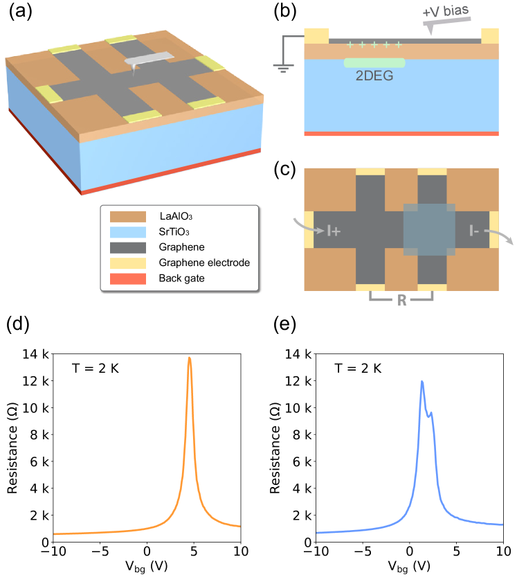
Figure 1(a,b) illustrate the c-AFM writing setup. Graphene is scanned with a conductive doped-silicon tip in contact mode with a contact force of 15 20 nN and scanning speed between 1 m/s and 10 m/s . The bias voltage applied on the tip is set to V (for creating a conductive LAO/STO interface) or V (for restoring an insulating LAO/STO interface while avoiding damage to grapheneAlaboson et al. (2011)). After each raster scan of the graphene area, the CNP of the graphene in the written region is shifted. The mechanism for shifting the CNP is believed to be essentially the same as for tuning the LAO/STO interface without grapheneHuang et al. (2015); Li et al. (2016); Bi et al. (2010). Under ambient conditions, when a positive voltage is applied to the tip while graphene is grounded, water molecules adsorbed on the graphene surface are dissociated into protons, transferred through the graphene and mediate the metal-insulator transition in the LAO/STO while contribute to a shift in the chemical potential in the graphene layerHuang et al. (2015); Bi et al. (2010); Brown et al. (2016); Hu et al. (2014). The CNP can be further shifted by dynamically changing the electron density in the LAO/STO layer.
STO has high dielectric permittivity at low temperature ()Weaver (1959), which enables the graphene to be easily tuned with a back-gate voltage applied to the bottom of the LAO/STO substrate (Figure 1(b)). However, this gating method is subject to significant hysteresisCouto, Sacépé, and Morpurgo (2011); Jnawali et al. (2017) (see Fig. S1(a), inset), and hence the back-gate voltage is not a reliable indicator of doping level with respect to the CNP. In addition, the c-AFM lithography itself will dope the graphene, even when the back-gate voltage is held fixed. For these reasons, we rely on the four-terminal resistance of the graphene to monitor the carrier density change in situ during the c-AFM writing process, which takes place under the condition V (more details are discussed in the supplementary materials). Once the c-AFM writing is finished, the sample is immediately stored in vacuum and cooled to cryogenic temperatures, where the writing is known to persist indefinitelyBi et al. (2010); Huang et al. (2015). To directly illustrate the effect of c-AFM writing, we scan half of the graphene device with V, as shown in Figure 1(c). The graphene resistance is then measured as a function of back-gate voltage at K. Figure 1(d) shows a control measurement where the resistance is measured before c-AFM scanning. The peak at V clearly indicates the CNP. Figure 1(e) is measured after c-AFM writing shown in Figure 1(c), and two peaks can be observed. The additional peak on the left-hand-side is attributed to the c-AFM writing.
The graphene doping from the positively biased c-AFM tip is reversible. After the c-AFM writing and the change in four-terminal resistance being observed, a scan with V voltage on the c-AFM tip will partially remove the previous writing effect. Scans with negative need to be carefully conducted and the c-AFM tip should be connected in series with a 1 G resistor, due to the fact that graphene can be oxidized as anodeAlaboson et al. (2011); Byun et al. (2011). Also, graphene has to be detached from measurement leads or groundings so that there is no significant current flowing through grapheneAlaboson et al. (2011).
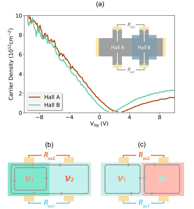
The carrier density in the LAO/STO-doped graphene device is quantified using the Hall effect. As shown in the inset of Figure 2(a), a graphene/LAO/STO device is prepared with one graphene Hall cross (Hall B) scanned under contact mode with the c-AFM tip biased at V for 15 times. A second Hall cross device (Hall A) is measured as a control, where no c-AFM lithography is performed. An electrical gate connected to the back of the 1 mm thick STO substrate is used to adjust the overall carrier density of the graphene device. Magnetotransport experiments are performed at K, in an out-of-plane magnetic field ( T), in order to determine the carrier densities of the two regions. A shift of cm-2 is observed, with the patterned area being more -type. Because Hall Device B is locally gated positively, the CNP is shifted to a lower value (green curve). The carrier densities on both regions can be tuned by the back-gate up to cm-2 at V, in part due to the large dielectric constant of STO () at 2 KWeaver (1959); Couto, Sacépé, and Morpurgo (2011). The right ends of the curves are less linear and tends to be saturated, due to the shielding effect of the 2DEG on LAO/STO interface induced by a high positive back-gate voltage. For V the interface of LAO/STO outside the previously written area is insulating, so the back-gate voltage will not be shielded.
At sufficiently large magnetic fields, graphene would exhibit quantized Hall resistance of and vanishing longitudinal resistance, as a result of the non-trivial Berry phase and four-fold degeneracy from electron spin and valley pseudo-spinNovoselov et al. (2004); Geim and Novoselov (2010); Zhang et al. (2005). When the two adjacent regions have different Landau level filling factors, for example a - junction in the quantum Hall regimeWilliams, DiCarlo, and Marcus (2007); Amet et al. (2014), the mixing and equilibration of edge states will produce a non-zero longitudinal resistance, which follows Landauer-Buttiker formalismBüttiker (1986, 1988). In our sample, the cm-2 carrier density difference on the two sides is enough to keep them at adjacent Landau level filling factors. Consequently, these two regions have different edge-channel occupancies. As shown in Figure 2(b), when both regions have the same polarity, the channels present in both regions would travel across both regions, while those ones from higher filling factors would only circulate in one region. The longitudinal resistance and measured from the top and bottom of the sample can be described using the Landauer-Buttiker formalismWilliams, DiCarlo, and Marcus (2007); Abanin and Levitov (2007); Amet et al. (2014); Büttiker (1986, 1988); Ki et al. (2010); Klimov et al. (2015); Woszczyna et al. (2011); Özyilmaz et al. (2007); Schmidt et al. (2013) (details of derivations can be found in the supplementary materials):
where and are the filling factors of the two regions, equal . In the case of opposite polarity on two sides the device becomes a - junction and the current flows in opposite directions on each side. The longitudinal resistance and become:
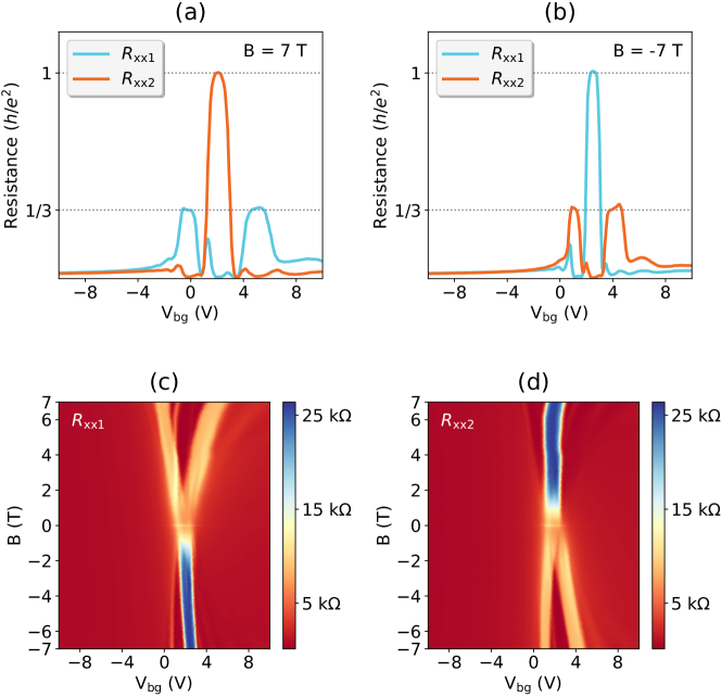
Figure 3(a) and 3(b) shows and in T and T magnetic fields. When the back gate is swept from V to V, the carrier type in the two regions would transit from unipolar (, ) to bipolar (, ) and then unipolar (, ) again. As shown in Figure 3(a), when the back-gate voltage is between V and V, the resistance transitions from to 0 and then to , while transitions from 0 to and then to 0, as predicted by the Landauer-Buttiker formalism. When the magnetic field is reversed, the quantization of and are switched, because of the reversing of current directions. Figure 3(c) and (d) shows the swapping of quantization between and when the magnetic field is reversed. These results are consistent with the graphene edge-state mixing reported in literatureSchmidt et al. (2013); Lohmann, von Klitzing, and Smet (2009). The values of resistance plateaus are quite close to theoretical values when the magnetic field is higher than 2 T, suggesting well-defined edge states equilibrium. The quantization features experience negligible change over the course of the measurement ( 10 hours), indicating that the graphene doping is stable in vacuum, similar to the c-AFM writing on bare LAO/STOBi et al. (2010).
In summary, we developed a reversible, spatially controllable graphene doping technique by c-AFM tips on LAO/STO substrates. Graphene edge state mixing in quantum Hall regime can be observed from with the c-AFM writing. In the future, this technique can be used locally dope high-mobility graphene with feature sizes as small as 20 nm Huang et al. (2015), to create a new family of reconfigurable graphene metamaterials.
This research was supported by the Office of Naval Research (N00014-16-1-3152), National Science Foundation and US-Israel Binational Science Foundation (DMR-1609519), and Vannevar Bush Faculty Fellowship program sponsored by the Basic Research Office of the ASD (R&E) and funded by the ONR (N00014-15-1-2847). The work at University of Wisconsin-Madison was supported by the National Science Foundation (DMR-1629270) and the Air Force Office of Scientific Research (FA9550-15-1-0334).
Supplementary material
See supplementary material for the details of hysteresis from back-gate voltage sweep, resistance and carrier density of graphene as functions of back-gate voltage, graphene resistance change during the c-AFM writing process, and the derivations of longitudinal resistances for edge-state mixing.
Acknowledgements.
This research was supported by the Office of Naval Research (N00014-16-1-3152), National Science Foundation and US-Israel Binational Science Foundation (DMR-1609519), and Vannevar Bush Faculty Fellowship program sponsored by the Basic Research Office of the ASD(R&E) and funded by the ONR (N00014-15-1-2847). The work at University of Wisconsin-Madison was supported by the National Science Foundation (DMR-1629270) and the Air Force Office of Scientific Research (FA9550-15-1-0334).References
- Cen et al. (2008) C. Cen, S. Thiel, G. Hammerl, C. Schneider, K. Andersen, C. Hellberg, J. Mannhart, and J. Levy, Nature Materials 7, 298 (2008).
- Huang et al. (2015) M. Huang, G. Jnawali, J.-F. Hsu, S. Dhingra, H. Lee, S. Ryu, F. Bi, F. Ghahari, J. Ravichandran, L. Chen, P. Kim, C.-B. Eom, B. D’Urso, P. Irvin, and J. Levy, APL Materials 3, 062502 (2015).
- Allain and Fuchs (2011) P. E. Allain and J.-N. Fuchs, The European Physical Journal B 83, 301 (2011).
- Katsnelson, Novoselov, and Geim (2006) M. Katsnelson, K. Novoselov, and A. Geim, Nature Physics 2, 620 (2006).
- Young and Kim (2009) A. F. Young and P. Kim, Nature Physics 5, 222 (2009).
- Shytov, Rudner, and Levitov (2008) A. V. Shytov, M. S. Rudner, and L. S. Levitov, Physical Review Letters 101, 156804 (2008).
- Williams, DiCarlo, and Marcus (2007) J. Williams, L. DiCarlo, and C. Marcus, Science 317, 638 (2007).
- Abanin and Levitov (2007) D. Abanin and L. Levitov, Science 317, 641 (2007).
- Lohmann, von Klitzing, and Smet (2009) T. Lohmann, K. von Klitzing, and J. H. Smet, Nano letters 9, 1973 (2009).
- Amet et al. (2014) F. Amet, J. Williams, K. Watanabe, T. Taniguchi, and D. Goldhaber-Gordon, Physical Review Letters 112, 196601 (2014).
- Gutiérrez et al. (2018) C. Gutiérrez, D. Walkup, F. Ghahari, C. Lewandowski, J. F. Rodriguez-Nieva, K. Watanabe, T. Taniguchi, L. S. Levitov, N. B. Zhitenev, and J. A. Stroscio, Science 361, 789 (2018).
- Ohtomo and Hwang (2004) A. Ohtomo and H. Hwang, Nature 427, 423 (2004).
- Brinkman et al. (2007) A. Brinkman, M. Huijben, M. Van Zalk, J. Huijben, U. Zeitler, J. Maan, W. G. van der Wiel, G. Rijnders, D. H. Blank, and H. Hilgenkamp, Nature Materials 6, 493 (2007).
- Caviglia et al. (2010) A. Caviglia, M. Gabay, S. Gariglio, N. Reyren, C. Cancellieri, and J.-M. Triscone, Physical Review Letters 104, 126803 (2010).
- Fischer, Raghu, and Kim (2013) M. H. Fischer, S. Raghu, and E.-A. Kim, New Journal of Physics 15, 023022 (2013).
- Shalom et al. (2010) M. B. Shalom, M. Sachs, D. Rakhmilevitch, A. Palevski, and Y. Dagan, Physical Review Letters 104, 126802 (2010).
- Reyren et al. (2007) N. Reyren, S. Thiel, A. Caviglia, L. F. Kourkoutis, G. Hammerl, C. Richter, C. Schneider, T. Kopp, A.-S. Rüetschi, D. Jaccard, et al., Science 317, 1196 (2007).
- Cheng et al. (2015) G. Cheng, M. Tomczyk, S. Lu, J. P. Veazey, M. Huang, P. Irvin, S. Ryu, H. Lee, C.-B. Eom, C. S. Hellberg, and J. Levy, Nature 521, 196 (2015).
- Thiel et al. (2006) S. Thiel, G. Hammerl, A. Schmehl, C. Schneider, and J. Mannhart, Science 313, 1942 (2006).
- Cen et al. (2009) C. Cen, S. Thiel, J. Mannhart, and J. Levy, Science 323, 1026 (2009).
- Cheng et al. (2011) G. Cheng, P. F. Siles, F. Bi, C. Cen, D. F. Bogorin, C. W. Bark, C. M. Folkman, J.-W. Park, C.-B. Eom, G. Medeiros-Ribeiro, and J. Levy, Nature Nanotechnology 6, 343 (2011).
- Jnawali et al. (2015) G. Jnawali, L. Chen, M. Huang, H. Lee, S. Ryu, J. P. Podkaminer, C.-B. Eom, P. Irvin, and J. Levy, Applied Physics Letters 106, 211101 (2015).
- Chen et al. (2019) L. Chen, E. Sutton, H. Lee, J.-W. Lee, J. Li, C.-B. Eom, P. Irvin, and J. Levy, Light: Science & Applications 8, 24 (2019).
- Annadi et al. (2018) A. Annadi, G. Cheng, H. Lee, J.-W. Lee, S. Lu, A. Tylan-Tyler, M. Briggeman, M. Tomczyk, M. Huang, D. Pekker, C.-B. Eom, P. Irvin, and J. Levy, Nano Letters 18, 4473 (2018).
- Pai et al. (2018a) Y.-Y. Pai, H. Lee, J.-W. Lee, A. Annadi, G. Cheng, S. Lu, M. Tomczyk, M. Huang, C.-B. Eom, P. Irvin, and J. Levy, Phys. Rev. Lett. 120, 147001 (2018a).
- Pai et al. (2018b) Y.-Y. Pai, A. Tylan-Tyler, P. Irvin, and J. Levy, Reports on Progress in Physics 81, 036503 (2018b).
- Chen et al. (2018) L. Chen, J. Li, Y. Tang, Y.-Y. Pai, Y. Chen, N. Pryds, P. Irvin, and J. Levy, Advanced Materials 30, 1801794 (2018).
- Schmidt et al. (2013) H. Schmidt, J. Rode, C. Belke, D. Smirnov, and R. J. Haug, Physical Review B 88, 075418 (2013).
- Velasco Jr et al. (2016) J. Velasco Jr, L. Ju, D. Wong, S. Kahn, J. Lee, H.-Z. Tsai, C. Germany, S. Wickenburg, J. Lu, T. Taniguchi, et al., Nano letters 16, 1620 (2016).
- Dhingra et al. (2014) S. Dhingra, J.-F. Hsu, I. Vlassiouk, and B. D’Urso, Carbon 69, 188 (2014).
- Li et al. (2016) J. Li, J.-F. Hsu, H. Lee, S. Tripathi, Q. Guo, L. Chen, M. Huang, S. Dhingra, J.-W. Lee, C.-B. Eom, P. Irvin, J. Levy, and B. D’Urso, arXiv preprint arXiv:1606.08802 (2016).
- Alaboson et al. (2011) J. M. Alaboson, Q. H. Wang, J. A. Kellar, J. Park, J. W. Elam, M. J. Pellin, and M. C. Hersam, Advanced Materials 23, 2181 (2011).
- Bi et al. (2010) F. Bi, D. F. Bogorin, C. Cen, C. W. Bark, J.-W. Park, C.-B. Eom, and J. Levy, Applied Physics Letters 97, 173110 (2010).
- Brown et al. (2016) K. A. Brown, S. He, D. J. Eichelsdoerfer, M. Huang, I. Levy, H. Lee, S. Ryu, P. Irvin, J. Mendez-Arroyo, C.-B. Eom, C. A. Mirkin, and J. Levy, Nature Communications 7, 10681 (2016).
- Hu et al. (2014) S. Hu, M. Lozada-Hidalgo, F. Wang, A. Mishchenko, F. Schedin, R. Nair, E. Hill, D. Boukhvalov, M. Katsnelson, R. Dryfe, et al., Nature 516, 227 (2014).
- Weaver (1959) H. Weaver, Journal of Physics and Chemistry of Solids 11, 274 (1959).
- Couto, Sacépé, and Morpurgo (2011) N. J. Couto, B. Sacépé, and A. F. Morpurgo, Physical Review Letters 107, 225501 (2011).
- Jnawali et al. (2017) G. Jnawali, M. Huang, J.-F. Hsu, H. Lee, J.-W. Lee, P. Irvin, C.-B. Eom, B. D’Urso, and J. Levy, Advanced Materials 29, 1603488 (2017).
- Byun et al. (2011) I.-S. Byun, D. Yoon, J. S. Choi, I. Hwang, D. H. Lee, M. J. Lee, T. Kawai, Y.-W. Son, Q. Jia, H. Cheong, et al., ACS Nano 5, 6417 (2011).
- Novoselov et al. (2004) K. S. Novoselov, A. K. Geim, S. V. Morozov, D. Jiang, Y. Zhang, S. V. Dubonos, I. V. Grigorieva, and A. A. Firsov, science 306, 666 (2004).
- Geim and Novoselov (2010) A. K. Geim and K. S. Novoselov, in Nanoscience and Technology: A Collection of Reviews from Nature Journals (World Scientific, 2010) pp. 11–19.
- Zhang et al. (2005) Y. Zhang, Y.-W. Tan, H. L. Stormer, and P. Kim, Nature 438, 201 (2005).
- Büttiker (1986) M. Büttiker, Physical Review Letters 57, 1761 (1986).
- Büttiker (1988) M. Büttiker, Physical Review B 38, 9375 (1988).
- Ki et al. (2010) D.-K. Ki, S.-G. Nam, H.-J. Lee, and B. Özyilmaz, Physical Review B 81, 033301 (2010).
- Klimov et al. (2015) N. N. Klimov, S. T. Le, J. Yan, P. Agnihotri, E. Comfort, J. U. Lee, D. B. Newell, and C. A. Richter, Physical Review B 92, 241301 (2015).
- Woszczyna et al. (2011) M. Woszczyna, M. Friedemann, T. Dziomba, T. Weimann, and F. J. Ahlers, Applied Physics Letters 99, 022112 (2011).
- Özyilmaz et al. (2007) B. Özyilmaz, P. Jarillo-Herrero, D. Efetov, D. A. Abanin, L. S. Levitov, and P. Kim, Physical Review Letters 99, 166804 (2007).