Influence of stoichiometry on interfacial conductance in \ceLaAlO3/\ceSrTiO3 grown by off-axis sputtering
Abstract
We report on the fabrication of conducting interfaces between \ceLaAlO3 and \ceSrTiO3 by off-axis sputtering in an Ar atmosphere. At a growth pressure of 0.04 mbar the interface is metallic, with a carrier density of the order of cm-2 at 3 K. By increasing the growth pressure, we observe an increase of the out-of-plane lattice constants of the LaAlO3 films while the in-plane lattice constants do not change. Also, the low-temperature sheet resistance increases with increasing growth pressure, leading to an insulating interface when the growth pressure reaches 0.10 mbar. We attribute the structural variations to an increase of the La/Al ratio, which also explains the transition from metallic behavior to insulating behavior of the interfaces. Our research emphasizes the key role of the cation stoichiometry of LaAlO3 in the formation of the conducting interface, and also the control which is furnished by the Ar pressure in the growth process.
pacs:
61.50.Nw, 73.40.-c, 81.15.CdThe discovery of a high mobility conducting interface between \ceLaAlO3 (LAO) and \ceSrTiO3 (STO) has given rise to numerous investigations Ohtomo and Hwang (2004). This two-dimensional electron system (2DES) exhibits multiple intriguing physical properties, such as superconductivity Reyren et al. (2007), magnetism Li et al. (2011); Bert et al. (2011); Lee et al. (2013), and gate tunable insulator to metal Thiel et al. (2006) and insulator to superconductor transitions Caviglia et al. (2008). However, the origin of the 2DES in still under debate. Proposed explanations basically fall into two classes, intrinsic charge transfer and extrinsic defects mechanisms. The intrinsic mechanism considers the polar discontinuity between the polar LAO and the nonpolar STO, which leads to a charge transfer above a critical thickness of LAO films Nakagawa et al. (2006). The extrinsic mechanisms involve defects formed at the interface during the film deposition process, such as oxygen vacancies in the STO substrate Kalabukhov et al. (2007); Siemons et al. (2007); Herranz et al. (2007) and cation intermixing at the interface Willmott et al. (2007); Chambers et al. (2010).
Pulsed laser deposition (PLD) is by far the most commonly used growth method to prepare LAO/STO interfaces. During the PLD process,high energy particle bombardment could introduce the above defects into the interface, which makes it difficult to understand the roles of the intrinsic and extrinsic mechanisms Chambers et al. (2010). Other growth techniques bring new insights here. Warusawithana et al. (2013) studied the LAO/STO system by molecular beam epitaxy (MBE). The interesting outcome is that interfacial conductivity was only observed in Al-rich samples (La/Al 0.97). Further density functional calculations demonstrated the different roles of defects in the charge transfer mechanism. In Al-rich samples, Al can fill La vacancies without changing the net charge of the (001) planes. The electronic reconstruction can still transfer electrons to the interface. In La-rich sample, however, La can not substitute for Al, resulting in the formation of \ceAl2O3-vacancy complexes which prohibits the charge transfer.
Sputtering also has been used. High-pressure () on-axis sputtering yielded LAO films with a La/Al ratio of ,and insulating interfaces Dildar et al. (2013). off-axis sputtering has been shown to be capable of growing epitaxial and smooth films with conducting interfaces Podkaminer et al. (2013). Sputtering is widely used in industry, which can also facilitate the device applications of LAO/STO interfaces. In this work, we show the growth of high quality epitaxial LAO films by off-axis sputtering. The La/Al ratio is tuned by varying the growth pressure. As a consequence, we observe strong but controlled variations in the interfacial conductivity.
LAO films were grown on \ceTiO2-terminated STO (001) substrates. In order to obtain the \ceTiO2 termination, the substrates were etched by buffered \ceHF for 30 and annealed at in flowing oxygen () for Koster et al. (1998). In the sputtering system, the working distances were from the surface of the heater to the axis of the target and from the surface of the target to the axis of the heater. It should be noted that the proper choice of growth pressure is strongly dependent on the working distances. A 2-inch single crystal LAO wafer was used as the sputtering target. The growth temperature was and the RF power was . Five samples were grown at various Ar pressures from to (see Table 1). In the following the samples will be referred to with their growth pressure. The target was pre-sputtered for at least in order to stabilize an oxygen background partial pressure produced by the target Podkaminer et al. (2013). After deposition, the samples were annealed in oxygen at for to remove the oxygen vacancies in the STO substrates. The samples were then cooled down to room temperature in the same oxygen atmosphere at a rate of /. The deposition rate decreases from at to at . Two reference samples were prepared to test the effectiveness of the oxygen annealing treatment. One sample is a bare STO substrate heated up to the growth temperature without film deposition. The other sample is an amorphous LAO/STO sample grown at room temperature at . Both samples were highly conductive, which indicates the presence of oxygen vacancies Schooley et al. (1964); Chen et al. (2011). The samples then underwent the above oxygen annealing treatment and were found to be insulating.
Surface topologies were measured by tapping mode atomic force microscopy (AFM). The epitaxial quality of the interface was characterized by scanning transmission electron microscopy (STEM). Film thicknesses and lattice constants were determined by high-resolution X-ray diffraction (HRXRD). Magnetrotransport properties were measured with a Quantum Design physical property measurement system (PPMS) by sweeping the magnetic field between . The measurements were performed in the van der Pauw geometry. Ohmic contacts were formed by wedge bonding Al wire directly to the sample surface.
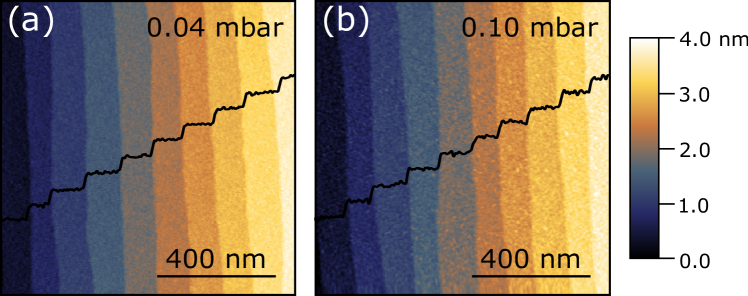
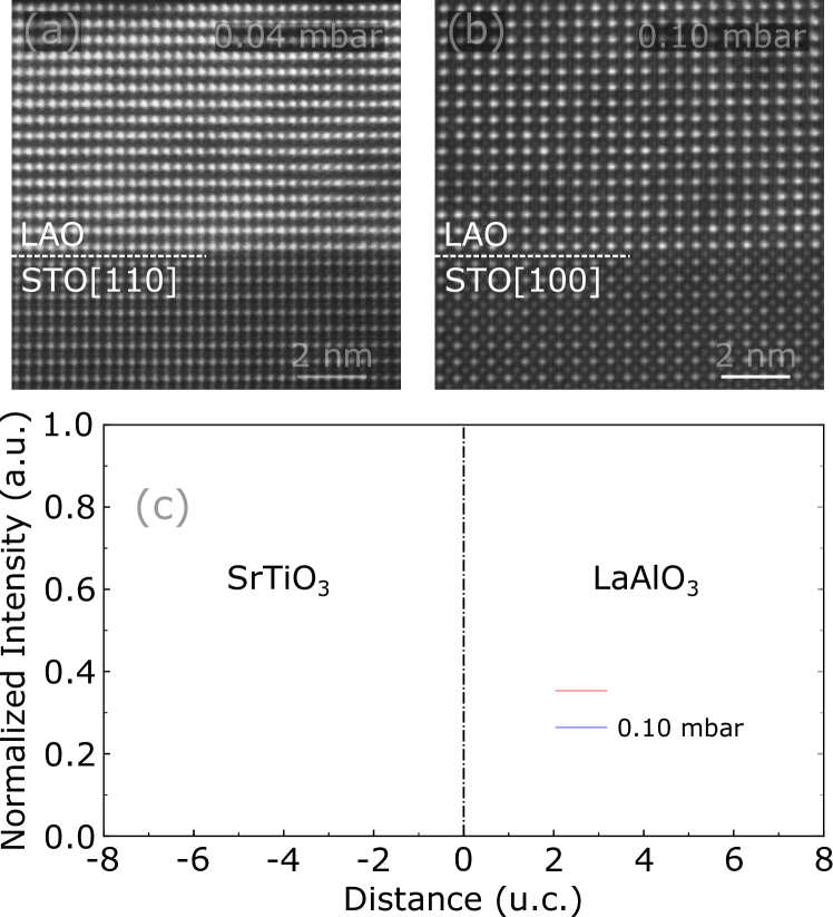
Fig. 1(a) and Fig. 1(b) show the AFM topographic images of samples 004 and 010. An atomically flat surface with clear step-and-terrace structure can be observed. The inset shows the step height which corresponds to the STO (001) interplanar distance ( ). The epitaxial quality of the films was further characterized by high-angle annular dark field STEM (HAADF-STEM). As shown in Fig. 2(a) and Fig. 2(b), atomically sharp interfaces between the film and the substrate are clearly visible. Fig. 2(c) shows the STEM electron energy loss spectroscopy (STEM-EELS) analysis of samples 004 and 010. This concentration profile is obtained by integration of the EELS intensity of the La-M4,5 and Ti-L2,3 edges during a spectrum image unit cell by unit cell in the growth direction. The profile is normalized by the maximum of intensity and cation vacancies are neglected. Identical intermixing (4 unit cells) was observed for both samples. This demonstrates that interdiffusion is a phenomenon that is not influenced by the growth pressure of the film.
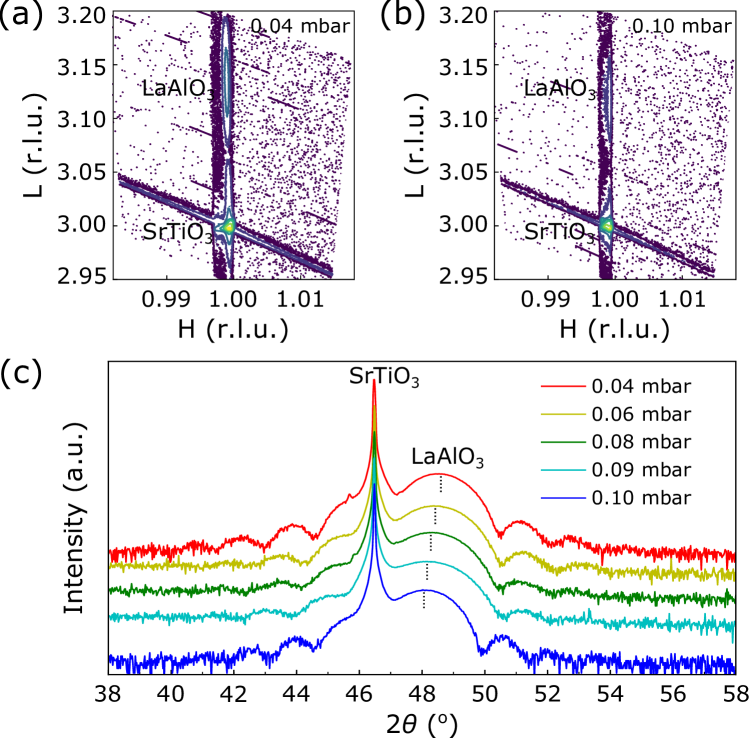
Fig. 3(a) and Fig. 3(b) show the reciprocal space maps (RSM) around the STO (103) diffraction peak of samples 004 and 010. The films are coherently strained to the substrate, which means that in-plane lattice constant () is . Fig. 3(c) shows the -2 scans. The dashed lines are the positions of LAO (002) diffraction peaks. It can be seen that as the growth pressure increases, the LAO peak shifts to lower angle, which corresponds to an increase of the out-of-plane lattice constant () Qiao et al. (2011). By fitting the interference fringes, we extract as well as the film thickness (). Table 1 summarizes the estimated values for , and of the samples. It has been reported that the increase of is due to the increase of the La/Al ratio in LAO films. The relationship between them was systematically studied by Qiao et al. (2011). Thus, we extract the La/Al ratios of our samples by interpolating our data points using their published results. The interpolated La/Al ratios are listed in Table 1. As the growth pressure increases from 0.04 mbar to 0.10 mbar, the La/Al ratio increases from 0.88 to 1.00.
| Growth Pressure | La/Al ratio111Interpolated La/Al ratios from Ref. Qiao et al. (2011). | |||
| (mbar) | (Å) | (Å) | (u.c.) | |
| ratio222Expected La/Al ratios from Ref. Qiao et al. (2011). | ||||
| 0.04 | 3.905 | 3.734 | 16 | 0.88 |
| 0.06 | 3.905 | 3.739 | 15 | 0.89 |
| 0.08 | 3.905 | 3.745 | 15 | 0.91 |
| 0.09 | 3.905 | 3.751 | 14 | 0.94 |
| 0.10 | 3.905 | 3.763 | 17 | 1.00 |
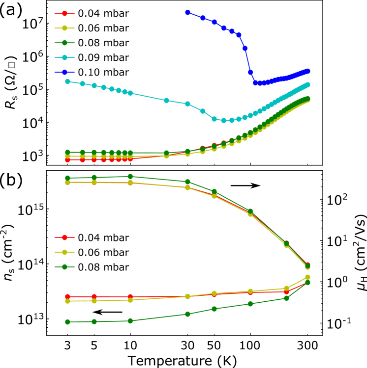
Fig. 4(a) shows the temperature dependence of the sheet resistance () for samples grown at various Ar pressures. Samples 004, 006 and 008 show similar metallic behavior from to . The interfacial conductivity changes dramatically as the growth pressure further increases. For sample 009, decreases from / at to / at and then gradually increases to / at . For sample 010, decreases from / at to / at and abruptly changes to insulating state afterwards. The temperature dependence of the carrier density () and the Hall mobility () for the metallic samples are shown in Fig. 4(b). and were determined by and , where and are the electron charge and the Hall coefficient, respectively. and are approximately and , respectively, at , which is consistent with reported results of LAO/STO interfaces grown by sputtering Podkaminer et al. (2013) and PLD Kalabukhov et al. (2007); Liu et al. (2013).
Our experimental results help to gain some insight in the role of extrinsic defects induced by the PLD process. First, as is well known, oxygen vacancies can lead to conductivity in either bare STO substrates Schooley et al. (1964) or LAO/STO interfaces Cancellieri et al. (2010); Chen et al. (2011); Liu et al. (2013). Our samples were grown in a reducing atmosphere, thus there is a large amount of oxygen vacancies in STO without post oxygen annealing. The behavior of our reference samples indicates that the post oxygen annealing treatment is efficient enough to remove the oxygen vacancies in the STO substrate created during the film deposition.
Second, it has been reported that La-doped STO shows metallic behavior Marina (2002). At the LAO/STO interface, La/Sr intermixing could be induced in two ways. One way is simply by the PLD process itself, during which the STO substrate is bombarded by particles with kinetic energies around several tens of Chambers et al. (2010). In our off-axis sputtering deposition, we use relatively high Ar pressures (0.04-0.10 ), which correspond to mean free paths of several millimeters. The direct distance between the center of the target and the substrate is about . The ejected particles would undergo multiple scatterings to slow down their speed before they deposit on the substrate. In our case, the chance of introducing La/Sr intermixing by high energy particle bombarding should be low. The other way is the dipole compensation mechanism proposed by Nakagawa et al. (2006), where a compensating dipole is produced by La/Sr intermixing to reduce the interface dipole energy. We observed identical intermixing in samples 004 and 010. However, intermixing should not be the origin of conductivity otherwise the two samples would show similar conducting behavior. We therefore conclude that oxygen vacancies or cation intermixing may exist at our LAO/STO interfaces, however, their contributions to the conductivity are negligible.
In our experiments, all the LAO films are epitaxially strained to STO substrates. Increasing the growth pressure only increases the La/Al ratio, which we believe is due to light Al being scattered more easily at higher pressures Dildar et al. (2013). The dramatic change in the transport properties is related to the change of cation stoichiometry of the LAO films. Thus our results agree with the cation stoichiometry mechanism proposed by Warusawithana et al. (2013). For the LAO/STO samples grown by PLD, it has been reported that a slight variation in growth parameters modifies the cation stoichiometry of LAO Golalikhani et al. (2013); Breckenfeld et al. (2013); Sato et al. (2013), also resulting in a dramatic change in the interfacial conductivity. However, the cation stoichiometry is not checked on a routine basis. It might explain the fact that samples from different PLD groups are often hardly comparable, although similar growth parameters are used.
In conclusion, high quality epitaxial LAO films were grown on STO (001) substrates by off-axis sputtering. While increasing the growth pressure, little structural variations have been observed, except for an increase of the out-of-plane lattice constant, which indicates an increase of the La/Al ratio. Metallic conducting interfaces were only found in Al-rich samples. Our results emphasize that cation stoichiometry in LAO films plays an important role in the formation of interfacial conductivity at the LAO/STO interfaces.
We thank Nikita Lebedev, Aymen Ben Hamida and Prateek Kumar for useful discussions and Giordano Mattoni, Jun Wang, Vincent Joly and Hozanna Miro for their technical assistance. We also thank Jean-Marc Triscone and his group for sharing their design of the sputtering system with us. This work is supported by the Netherlands Organisation for Scientific Research (NWO). C. Yin is supported by China Scholarship Council (CSC) with grant No. 201508110214. N.G., D.K. and J.V. acknowledge financial support from the GOA project “Solarpaint” of the University of Antwerp.
References
- Ohtomo and Hwang (2004) A. Ohtomo and H. Y. Hwang, Nature 427, 423 (2004).
- Reyren et al. (2007) N. Reyren, S. Thiel, A. D. Caviglia, L. F. Kourkoutis, G. Hammerl, C. Richter, C. W. Schneider, T. Kopp, A.-S. Ruetschi, D. Jaccard, M. Gabay, D. A. Muller, J.-M. Triscone, and J. Mannhart, Science 317, 1196 (2007).
- Li et al. (2011) L. Li, C. Richter, J. Mannhart, and R. C. Ashoori, Nature Physics 7, 762 (2011).
- Bert et al. (2011) J. A. Bert, B. Kalisky, C. Bell, M. Kim, Y. Hikita, H. Y. Hwang, and K. A. Moler, Nature Physics 7, 767 (2011).
- Lee et al. (2013) J.-S. Lee, Y. W. Xie, H. K. Sato, C. Bell, Y. Hikita, H. Y. Hwang, and C.-C. Kao, Nature Materials 12, 703 (2013).
- Thiel et al. (2006) S. Thiel, G. Hammerl, A. Schmehl, C. W. Schneider, and J. Mannhart, Science 313, 1942 (2006).
- Caviglia et al. (2008) A. D. Caviglia, S. Gariglio, N. Reyren, D. Jaccard, T. Schneider, M. Gabay, S. Thiel, G. Hammerl, J. Mannhart, J.-M. Triscone, and et al., Nature 456, 624– (2008).
- Nakagawa et al. (2006) N. Nakagawa, H. Y. Hwang, and D. A. Muller, Nature Materials 5, 204 (2006).
- Kalabukhov et al. (2007) A. Kalabukhov, R. Gunnarsson, J. Börjesson, E. Olsson, T. Claeson, and D. Winkler, Physical Review B 75, 121404(R) (2007).
- Siemons et al. (2007) W. Siemons, G. Koster, H. Yamamoto, W. A. Harrison, G. Lucovsky, T. H. Geballe, D. H. A. Blank, and M. R. Beasley, Physical Review Letters 98, 196802 (2007).
- Herranz et al. (2007) G. Herranz, M. Basletić, M. Bibes, C. Carrétéro, E. Tafra, E. Jacquet, K. Bouzehouane, C. Deranlot, A. Hamzić, J.-M. Broto, and et al., Physical Review Letters 98, 216803 (2007).
- Willmott et al. (2007) P. R. Willmott, S. A. Pauli, R. Herger, C. M. Schlepütz, D. Martoccia, B. D. Patterson, B. Delley, R. Clarke, D. Kumah, C. Cionca, and et al., Physical Review Letters 99, 155502 (2007).
- Chambers et al. (2010) S. Chambers, M. Engelhard, V. Shutthanandan, Z. Zhu, T. Droubay, L. Qiao, P. Sushko, T. Feng, H. Lee, T. Gustafsson, and et al., Surface Science Reports 65, 317 (2010).
- Warusawithana et al. (2013) M. P. Warusawithana, C. Richter, J. A. Mundy, P. Roy, J. Ludwig, S. Paetel, T. Heeg, A. A. Pawlicki, L. F. Kourkoutis, M. Zheng, M. Lee, B. Mulcahy, W. Zander, Y. Zhu, J. Schubert, J. N. Eckstein, D. A. Muller, C. S. Hellberg, J. Mannhart, and D. G. Schlom, Nature Communications 4, 2351 (2013).
- Dildar et al. (2013) I. M. Dildar, D. B. Boltje, M. H. S. Hesselberth, J. Aarts, Q. Xu, H. W. Zandbergen, and S. Harkema, Applied Physics Letters 102, 121601 (2013).
- Podkaminer et al. (2013) J. P. Podkaminer, T. Hernandez, M. Huang, S. Ryu, C. W. Bark, S. H. Baek, J. C. Frederick, T. H. Kim, K. H. Cho, J. Levy, and et al., Applied Physics Letters 103, 071604 (2013).
- Koster et al. (1998) G. Koster, B. L. Kropman, G. J. H. M. Rijnders, D. H. A. Blank, and H. Rogalla, Applied Physics Letters 73, 2920 (1998).
- Schooley et al. (1964) J. F. Schooley, W. R. Hosler, and M. L. Cohen, Physical Review Letters 12, 474–475 (1964).
- Chen et al. (2011) Y. Chen, N. Pryds, K. J. E., G. Koster, J. Sun, E. Stamate, B. Shen, G. Rijnders, and S. Linderoth, Nano Letters 11, 3774– (2011).
- Qiao et al. (2011) L. Qiao, T. C. Droubay, T. Varga, M. E. Bowden, V. Shutthanandan, Z. Zhu, T. C. Kaspar, and S. A. Chambers, Physical Review B 83, 085408 (2011).
- Liu et al. (2013) Z. Q. Liu, C. J. Li, W. M. Lü, X. H. Huang, Z. Huang, S. W. Zeng, X. P. Qiu, L. S. Huang, A. Annadi, J. S. Chen, and et al., Physical Review X 3, 021010 (2013).
- Cancellieri et al. (2010) C. Cancellieri, N. Reyren, S. Gariglio, A. D. Caviglia, A. Fete, and J.-M. Triscone, EPL (Europhysics Letters) 91, 17004 (2010).
- Marina (2002) O. Marina, Solid State Ionics 149, 21–28 (2002).
- Golalikhani et al. (2013) M. Golalikhani, Q. Y. Lei, G. Chen, J. E. Spanier, H. Ghassemi, C. L. Johnson, M. L. Taheri, and X. X. Xi, Journal of Applied Physics 114, 027008 (2013).
- Breckenfeld et al. (2013) E. Breckenfeld, N. Bronn, J. Karthik, A. R. Damodaran, S. Lee, N. Mason, and L. W. Martin, Physical Review Letters 110, 196804 (2013).
- Sato et al. (2013) H. K. Sato, C. Bell, Y. Hikita, and H. Y. Hwang, Applied Physics Letters 102, 251602 (2013).