Finding a junction partner for candidate solar cell absorbers enargite and bournonite from electronic band and lattice matching
Abstract
An essential step in the development of a new photovoltaic (PV) technology is choosing appropriate electron and hole extraction layers to make an efficient device. We recently proposed the minerals enargite (Cu3AsS4) and bournonite (CuPbSbS3) as materials that are chemically stable with desirable optoelectronic properties for use as the absorber layer in a thin-film PV device. For these compounds, spontaneous lattice polarization with internal electric fields — and potential ferroelectricity — may allow for enhanced carrier separation and novel photophysical effects. In this work, we calculate the ionization potentials for non-polar surface terminations and propose suitable partners for forming solar cell heterojunctions by matching the electronic band edges to a set of candidate electrical contact materials. We then further screen these candidates by matching the lattice constants and identify those that are likely to minimise strain and achieve epitaxy. This two-step screening procedure identified a range of unconventional candidate contact materials including SnS2, ZnTe, WO3, and Bi2O3.
I Introduction
Solar power is an attractive source of sustainable electricity. Technological breakthroughs to enable high-efficiency photovoltaic (PV) devices without the need to use scarce material components and with low manufacturing costs would secure solar power as a future power source. Exploiting non-centrosymmetry and lattice polarization in ‘photoferroic’ materials could provide new pathways to high-efficiency PV devices. Phenomena referred to as ‘anomalous’ and ‘bulk’ PV effects in polar materials have demonstrated photovoltages orders of magnitude greater than the optical band gap and photocurrents in bulk, single-crystal absorbers in the absence of a typical p-n junction for carrier separation Fridkin and Popov (1978); Ruppel, Baltz, and Wurfel (1982); Butler, Frost, and Walsh (2015) . On-going research efforts are exploring the theory behind these observed phenomena Young and Rappe (2012); Heyszenau (1978); Wang and Rappe (2015); Lopez-Varo et al. (2016).
We recently identified three naturally-ocurring minerals as candidate photoferroic materials based on their optical band gaps and polar crystal structures Wallace et al. (2017), including enargite (Cu3AsS4) and bournonite (CuPbSbS3) . To our knowledge, to date only one study has made solar cells out of any of these materials. In Ref. 9, solar cells were made from solution processed enargite using a device architecture developed for Cu(In,Ga)Se2 (CIGS) solar cell technology. In this study the authors list non-optimal band alignment of the absorber layer with the device architecture as a likely limitation of the current solar cell performance. This is also the case for CuSbS2 solar cells using device architecture optimised for CIGS absorber layers Whittles et al. (2017). Mature technologies, such as CIGS-based devices, are still being optimised through improved band alignment with the n-type buffer layer Larsson et al. (2017) and non-optimal band alignment is also being considered as a limiting factor on the performance of Cu2ZnSn(S,Se)4-based solar cells Crovetto and Hansen (2017). The optimization of device architecture for a new solar cell technology is a challenging and time-consuming process.
For many of the materials being studied for use as absorber layers in thin-film solar cells, such as chalcogenide semiconductors, it is not possible, or is very difficult, to achieve ambipolar doping. Therefore to achieve a p-n junction for many thin-film PV devices it is necessary to form an interface between materials with different optical band gaps, lattice constants and even crystal structures Klein (2015). In the extreme case when the two materials are poorly matched, differences in lattice constant and crystal structure at a heterojunction interface can introduce a large strain, resulting in poor epitaxy Butler et al. (2016a). Even for less extreme differences, small lattice mismatch at an interface generally introduces intra band gap defect states, which enhances Shockley-Read-Hall recombination, increasing dark currents, and reducing the open-circuit voltage of the device Nelson (2003).
In this work, we aim to accelerate the optimisation of solar cell device architectures for enargite (Cu3AsS4) and bournonite (CuPbSbS3) by screening for candidate junction partners that could have optimal electronic band offsets and crystal lattices well-matched to minimise strain at the interface. The principles behind our screening criteria for optimal band offsets are outlined in the next section. Where there is no literature consensus as to whether the material is likely to be more easily doped p-type or n-type we screen for candidate contacts based on the relevant band offset for forming a solar cell junction for both cases.
II Band offsets for solar cell heterojunctions
The band alignment at a solar cell junction is crucial to facilitate the separation of photo-excited electrons and holes to allow for extraction of the charge carriers before recombination can occur Heeger (2013). Although internal electric fields in the materials in this study may allow for a bulk photovoltaic effect for thin films (where the electrical asymmetry at a junction is not required for a photocurrent to be generated), a heterojunction would provide a global driving force for carrier collection at electrodes, while internal electric fields from the polar crystal structure could enhance carrier separation locally.
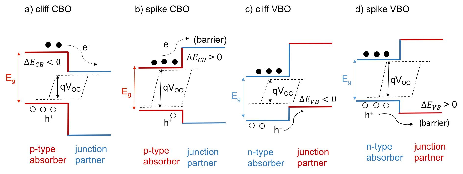
Semiconductor junctions are classified as type I, II or III based on the band alignment; however only type I and type II are of interest for PV applications. A type II ‘staggered’ junction can also be referred to as a ‘cliff-like’ offset and a type I ‘straddling’ junction can also be referred to as a ‘spike-like’ offset, as illustrated schematically in Fig 1. For a p-type absorber layer, the minority carriers are electrons promoted into the conduction band (CB) of the absorber. Therefore, the transport of electrons from the CB of the p-type absorber to the junction partner is important for determining device performance. The parameter of interest here is the conduction band offset (CBO) between the two materials. However, for n-type absorbers it is photoexcited holes that are the minority carriers and so it is the magnitude of the valance band offset (VBO) between the n-type absorber and the junction partner that is important for charge extraction.
It has been observed that for the p-type absorbers CIGS and CdTe, a spike offset (CBO within the range 0.1–0.3 eV), as shown in Fig. 1a, gives better device performance Song, Kanevce, and Sites (2016); Gloeckler and Sites (2005). Here, a small positive spike CBO creates an absorber inversion layer, resulting in a large hole barrier at the interfaceSong, Kanevce, and Sites (2016). The modest barrier to electron transfer means that electrons may still tunnel across the interface and be collectedNelson (2003). Electron-hole recombination at an interface with high defect densities is then thought to be suppressed due to an insufficient hole supply. In contrast, for a cliff offset where the CBO is negative, as shown in Fig 1b, there may be high concentrations of holes in the vicinity of the interface to assist interface recombination, thereby reducing the open-circuit voltage Song, Kanevce, and Sites (2016).
For the n-type absorber ZnSnN2 the opposite trend has been observed, where a spike VBO is expected to give a poorer performance Arca et al. (2018). Here, a spike offset limits transport across the interface due to the larger effective mass of minority-carrier holes (compared to CIGS and CdTe Marple (1963)) and associated lower hole mobility Arca et al. (2018). For ZnSnN2, a small cliff is thought to be optimal. In this study, we use calculated effective masses to inform our choice of optimal band offsets for forming solar cell heterojunctions.
III Methodology
III.1 Electronic band and lattice matching
Screening for candidate heterojunction partners based on electronic band offsets and minimum lattice strain is conducted using the methodology and dataset of tabulated ionization potentials (IPs) and electron affinities (EAs) for candidate junction partners in Ref. 16 and ElectronLatticeMatch libraries Butler . This dataset currently contains the electronic band gaps, IPs and EAs of 173 candidate heterojunction partners obtained either from experimental measurements or electronic structure calculations.
For p-type (n-type) absorbers we screen for candidate junction partners based on the CBO (VBO). We look for a small cliff offset by selecting a band offset in the range 0 to -0.3 eV. However for cases where the minority carrier effective mass calculated in Ref. 8 is less than 0.5 we also look for a small spike offset in the range +0.1 to +0.3 eV. For CIGS +0.2 eV has been reported to be optimal Gloeckler and Sites (2005) and +0.3 eV for CdTe Song, Kanevce, and Sites (2016).
We further limit our search to candidate junction partners where an interface with lattice strain less than 4% is obtained. We consider no defect states at the interface and allow no chemical intermixing, which is known to be present to a large extent at the CdTe:CdS contact Ohata, Saraie, and Tanaka (1973); Park et al. (2016). For final candidate contacts we estimate the likely extent of interface intermixing based on the chemical similarities of the components of the two materials forming the heterojunction.
III.2 Band alignment
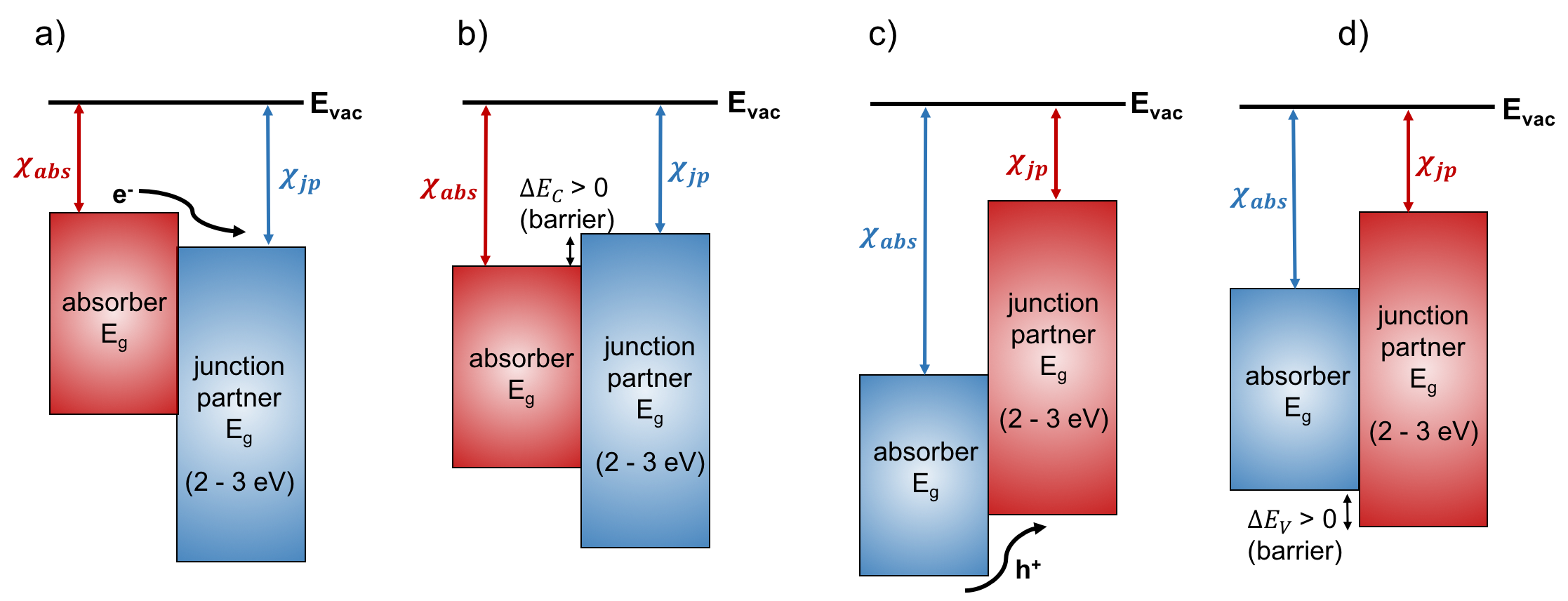
The alignment of the valence band energy to a common vacuum level, i.e. the ionization potential (IP), can be peformed using techniques such as photoelectron spectroscopy or Kelvin probe microscopy and can be computed using first-principles calculations of surface slab models Kumagai et al. (2017). The electron affinity () is the conduction band energy with respect to the vacuum level, which can be obtained by adding the value of the electronic band gap onto the IP of a material. Results from two decades of photoelectron spectroscopy experiments on CdTe and CIGS thin-film solar cells have been compared to density functional theory (DFT) calculations Klein (2015), where it was found that the energy band alignments for many interfaces were in good agreement. Theoretically predicted band alignments are usually the ‘intrinsic’ or ‘natural’ alignment for a particular combination of materials forming an interface Klein (2015), i.e. in the absence of defects, interfacial reconstructions, or thermal effects.Monserrat et al. (2018) This ideal band alignment therefore acts as a starting point to limit the search space for suitable junction partners.
The model used to predict the energy band alignment at solar cell heterojunctions in this study is the electron affinity rule (also known as Anderson’s rule) where energies are aligned through the vacuum level Anderson (1960); Butler et al. (2016b). The vacuum level of the two heterojunctions either side of the heterojunction are aligned to the same energy, the difference between the distance between the CBM and the vacuum () of each material is used to predict the CBO, as shown in Eq. 1.
We take semiconductor 1 to be the absorber with a band gap () within the visible range (approximately 1.1–1.7 eV) and semiconductor 2 to be the transparent junction partner with a wider in the range of 2–3 eV. The conduction band offset is defined as:
| (1) |
Similarly, the valence band offset is determined through the difference in the ionization potentials ():
| (2) |
A negative or corresponds to a cliff CBO or cliff VBO respectively, this is then a ‘staggered gap’. These different cases are illustrated in Fig. 2.
III.3 Computational details
III.3.1 Surface slab models
Band energies are dependent upon the surface terminations of a crystal. We therefore construct slab models for all possible non-polar surface terminations of the materials using the algorithm described in Ref. 30. Symmetric slab models are then cut from relaxed unit cells; visualisations of the slab structures are given in the SI.
For the relaxation of the ion positions and volume of the unit cells, calculations are performed in VASP Kresse and Furthmüller (1996a, b) using the PBEsol functional Csonka et al. (2009), projector augmented wave core potentialsBlöchl (1994), without including spin-orbit coupling (SOC) and with symmetry fixed until forces on the atoms are converged to within 0.005 eV per Å. A plane wave cutoff energy of 350 eV is used and k-grid densities of and were used to sample the electronic Brillouin zone for a 16 atom unit cell of enargite (Cu3AsS4) and a 24 atom unit cell of bournonite (CuPbSbS3), repectively.
To inform our later discussion for which candidate junction partners are likely to be the most important for devices, we calculate the surface energies for the slab models using Eq. 3 where is the total energy of the bulk crystal per formula unit, is the number of formula units in the surface slab and is the area of surface, of which there are two per slab model.
| (3) |
III.3.2 Ionization potential and electron affinity
Calculations for planar averaged electrostatic potential of the slab models are also performed in VASP but using the HSE06 functional Heyd, Scuseria, and Ernzerhof (2003) with SOC and a single k-point is used to sample the slab along the finite dimension. To calculate the ionization potentials of the surface slab models a macroscopic average technique is used. Kumagai et al. (2017) The difference between the macroscopic average of the vacuum potential and the bulk-like region of the surface slab is used to obtain the surface dipole shift, . The ionization potential is then calculated using the eigenvalue of the valence band maximum () for the bulk crystal:
| (4) |
Electron affinities, , are then calculated from the IP using the electronic band gap calculated with the HSE06 functional.
IV Results and discussion
IV.1 Electronic matching of junction partners
The band energies calculated for each material are summarised in Table 1. We find a notable variation in the IP for different surface terminations of the same material, which may have implications for the simplicity of the junction fabrication, especially as the low energy surface terminations have significantly different IPs. From inspection of the slab geometries (shown in the SI), slab models with larger IPs have denser surface structures with anion-rich terminations that could be associated with a larger double layer.Bardeen (1936)
| Absorber | Termination | Eg | IP | ||
| (100) | 1.32 | 4.97 | 3.64 | 0.050 | |
| Enargite | (010)a | 1.32 | 5.21 | 3.89 | 0.025 |
| (Cu3AsS4) | (010)b | 1.32 | 6.23 | 4.91 | 0.120 |
| (110) | 1.32 | 4.95 | 3.63 | 0.070 | |
| Bournonite (CuPbSbS3) | (100) | 1.68 | 5.61 | 3.93 | 0.042 |
| (010)a | 1.68 | 5.20 | 3.52 | 0.150 | |
| (010)b | 1.68 | 5.21 | 3.53 | 0.106 | |
| (110)a | 1.68 | 6.50 | 4.82 | 0.090 | |
| (110)b | 1.68 | 6.04 | 4.36 | 0.037 |
Experimental data for enargite suggests that the material exhibits native p-type conductivity Pauporte and Lincot (1995); Durant and Parkinson (2016). For bournonite, there is variation in the literature between experimental measurements on natural samples measuring n-type conductivity Durant and Parkinson (2016) and theoretical prediction of the defect physics suggesting the material will be intrinsically p-type and difficult to dope n-type Faghaninia et al. (2017). Junction partners for enargite are screened based on the CBO only, while for bournonite the CBO and VBO are considered in turn to provide options for an p-type or n-type absorber layer. We screen for both cliff and spike CBO for p-type bournonite, but only for a cliff VBO for n-type bournonite due to calculated heavy hole mass ()Wallace et al. (2017) in line with our earlier discussion.
IV.2 Low strain junctions
Candidates passing the electronic matching stage were screened for those with less than 4% lattice strain. Candidates containing Fe were not considered further as Fe is often associated with fast non-radiative recombination in solar cells due to possible excitations and recombination channels from a half occupied d-shell (d5 for Fe3+ and d6 for Fe2+). Where multiple structure files for the candidates were available on the Materials Project database Jain et al. (2013), unit cells for the most stable structures were preferentially selected for this lattice matching step, based on energy above the thermodynamic convex hull. All candidates considered in this second screening stage, including the materials project ID for the corresponding structure file, can be found in the SI.
Each surface slab termination was screened individually starting from the tabulated data for 173 candidate heterojunction partners. The remaining candidates after the two-step screening process for each surface model are listed in Tables 2 and 3 for bournonite and enargite, respectively. Averaged in-plane interface strain for all low-strain electronically-matched candidate junction partners are also reported. A selection of band alignment plots are shown in Figures 3 and 4; all other slab terminations are included in the SI. In each case, the candidate junction partner with the lowest interface strain is highlighted.
| Spike conduction band offset | Cliff conduction band offset | Cliff valence band offset | |||||||
| Surface | Candidate | (hkl) | Strain | Candidate | (hkl) | Strain | Candidate | (hkl) | Strain |
| Ce2O3 | (011), (101), (110) | 1.23% | |||||||
| GaP | (011), (101), (110) | 1.01% | |||||||
| (100) | SiC | (010), (100) | 0.73% | ||||||
| SnS2 | (110) | 0.67% | |||||||
| ZnSe | (001), (010), (100) | 0.83% | |||||||
| La2S3 | (110) | 0.71% | Ce2S3 | (001) | 1.71% | AlP | (011), (101), (110) | 0.71% | |
| (010)a | Nd2S3 | (001) | 0.10% | Cu2O | (011), (101), (110) | 0.81% | MoO3 | (100) | 0.23% |
| Sm2S3 | (001) | 2.28% | Gd2S3 | (011) | 0.71% | CuI | (110) | 2.73% | |
| WO3 | (110) | 0.49% | ZnTe | (001), (010), (100) | 0.75% | ||||
| La2S3 | (110) | 0.71% | Ce2S3 | (001) | 1.71% | AlP | (011), (101), (110) | 0.71% | |
| (010)b | Nd2S3 | (001) | 0.10% | Cu2O | (011), (101), (110) | 0.81% | MoO3 | (100) | 0.23% |
| Sm2S3 | (001) | 2.28% | Gd2S3 | (011) | 0.71% | CuI | (110) | 2.73% | |
| WO3 | (110) | 0.49% | ZnTe | (001), (010), (100) | 0.75% | ||||
| As2S3 | (101) | 0.90% | Ce2O3 | (011), (101), (110) | 0.68% | ||||
| Bi2O3 | (100) | 1.60% | GaP | (011), (101), (110) | 1.35% | ||||
| (110)a | CoTiO3 | (110) | 1.03% | SnS2 | (010), (100) | 0.94% | |||
| NiTiO3 | (110) | 1.08% | WO3 | (010) | 1.00% | ||||
| Zn3In2S6 | (110) | 0.09% | |||||||
| Dy2S3 | (110) | 1.47% | |||||||
| SiC | (110) | 1.47% | |||||||
| GaP | (011), (101), (110) | 1.35% | As2S3 | (101) | 0.90% | Nd2S3 | (110) | 0.64% | |
| SnS2 | (101), (100) | 0.94% | Bi2O3 | (100) | 1.60% | Sm2S3 | (110) | 0.70% | |
| (110)b | CdS | (110) | 2.17% | Tb2S3 | (110) | 1.71% | |||
| CoTiO3 | (110) | 1.03% | ZnTe | (011), (101), (110) | 0.43% | ||||
| PbO | (110) | 1.67% | |||||||
IV.2.1 Junction partners for bournonite
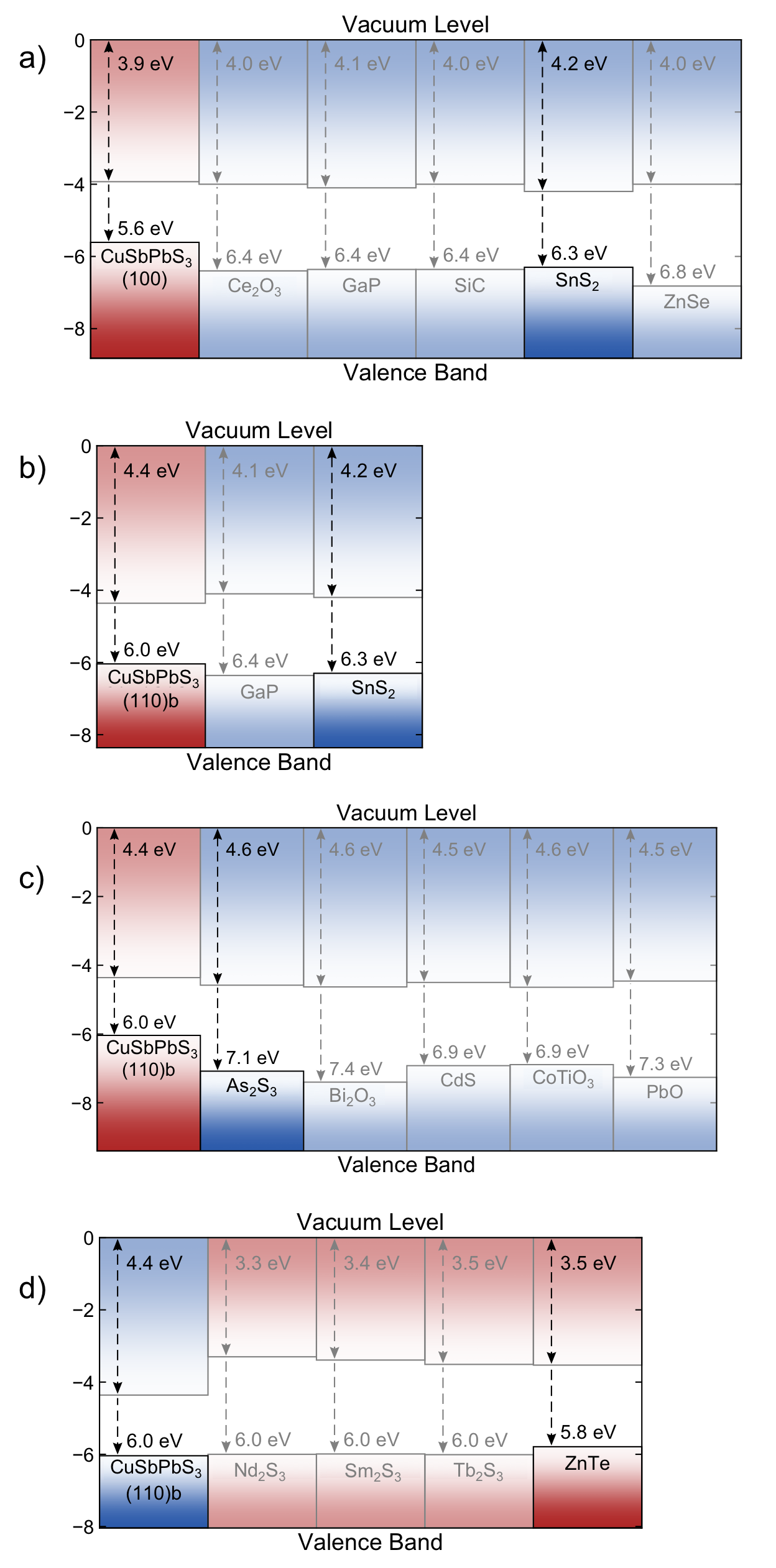
The lowest energy surfaces for bournonite were for the (100) and (110)b terminations, see Table 1. For the bournonite (100) surface, we were only able to find low-strain partners for a CBO cliff, which is relevant for bournonite as a p-type absorber. Table 2 and Fig. 3a show several options for junction partners. SnS2 is found to be the minimum strain candidate for the (100) surface. A further consideration is the simplicity of junction fabrication. Candidate junction partners able to produce a low-strain interface for multiple facets of the junction partner may imply more robust synthesis. For this reason, GaP and Ce2O3 are highlighted as alternative options.
For bournonite (110)b, we identified candidate junction partners for a spike CBO, cliff CBO, and cliff VBO. Candidate junction partners containing rare-earth elements such as Sm, Tb or Dy are less desirable for practical devices. SnS2 again emerges as a promising option for a spike CBO, Bi2O3 for a low-toxicity cliff CBO, and ZnTe for a cliff VBO for bournonite as an n-type absorber.
Overall, for bournonite SnS2 appears to be a promising junction partner for bournonite as a p-type absorber for both terminations and ZnTe for bournonite as an n-type absorber. It is possible that there could be significant intermixing between a S containing absorber and a Te containing junction partner, as has been observed at the CdTe:CdS interface,Ohata, Saraie, and Tanaka (1973) which would require careful processing and may change the nature of the band offsets.
IV.2.2 Junction partners for enargite
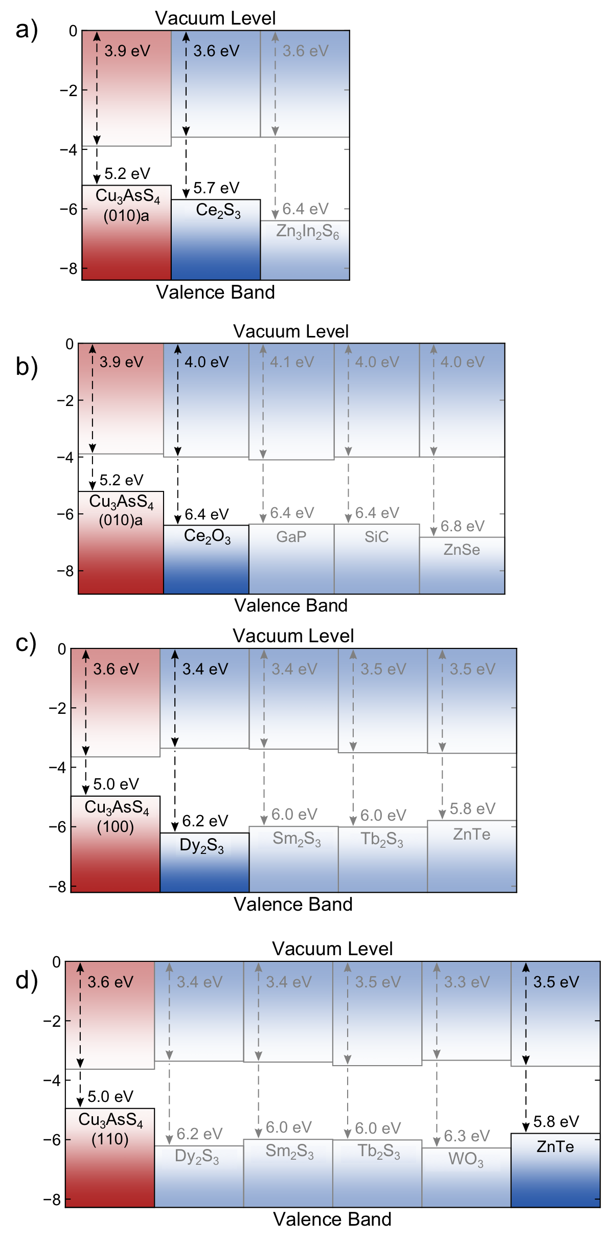
For enargite, the (010)a termination is the lowest energy with the next being the (100) and (110) terminations with similar energies, see Table 1. We note that although CdS is in our database of candidate junction partners, it did not make it through the screening process. This is likely a contributing factor to the low open-circuit voltage of enargite solar cells fabricated with CdS as the junction partner in Ref. 9.
For the minimum energy (010)a termination of enargite, junction partners with low strain were found for both a cliff and a spike CBO, Table 3. For this termination, Ce2O3 and Ce2S3 produced the lowest strain interfaces for a cliff and spike CBO, respectively. For the (100) and (110) terminations of enargite, only low-strain candidates were found for a spike CBO but both terminations had a similar list of candidate junction partners. Dy2S3 produced the lowest strain interface with the enargite (100) surface. However, due to the rarity of Dy, Sm and Tb, we regard candidates containing these elements as less desirable. ZnTe is a more promising candidate for the (100) termination. For the (110) surface, ZnTe is the minimum strain candidate, with WO3 being another viable option. ZnTe is likely to be the most robust choice owing to the similar matching to the (100) and (110) surface of enargite, again providing that significant interface mixing or defect formation does not occur.
| Surface | Candidate | (hkl) | Strain | ||
|---|---|---|---|---|---|
| (100) spike CBO | Dy2S3 | (001) | 0.81% | ||
| Sm2S3 | (001) | 1.43% | |||
| Tb2S3 | (001) | 1.10% | |||
| ZnTe | (011), (101), (110) | 1.01% | |||
| (010)a spike CBO | Ce2S3 | (001) | 1.05% | ||
| Zn3In2S6 | (110) | 1.19% | |||
| (010)a cliff CBO | Ce2O3 | (001), (010), (100) | 0.20% | ||
| GaP | (001), (010), (100) | 0.83% | |||
| SiC | (010), (100) | 1.33% | |||
| ZnSe | (001), (010), (100) | 2.02% | |||
|
Bi2O3 | (101) | 0.75% | ||
| (110) spike CBO | Dy2S3 | (011), (101) | 0.68% | ||
| Sm2S3 | (001) | 1.15% | |||
| Tb2S3 | (011), (101) | 0.98% | |||
| WO3 | (011) | 0.33% | |||
| ZnTe | (011), (101), (110) | 0.19% |
V Conclusions
The aim of this study has been to provide a route forward for the development of solar cell technologies based on enargite and bournonite. By using a combination of data-mining and first-principles calculations, we have identified promising photovoltaic heterojunction partners for low-index surface terminations of Cu3AsS4 and CuPbSbS3. The candidate partner materials include SnS2, ZnTe, WO3, and Bi2O3.
One aspect not covered in this report is the potential photoferroic nature of these absorber materials and devices. Internal electric fields in polar semicondictors may suppress electron-hole recombination by enhanced local carrier separationLopez-Varo et al. (2016) to provide a means of achieving high-efficiency solar cells. The orientation of electric polarisation may influence the direction of charge transport and collection — as has been explored in photoanodes for photoelectrochemical water splitting applications Yang et al. (2015). These factors could determine the optimal growth and contact orientations for maximising solar conversion efficiencies. Further work is required in this direction both in terms of atomistic and device modelling for non-conventional photovoltaic architectures.
Acknowledgements.
We thank Ji-Sang Park and Lee Burton for useful discussions. This work has been supported by the EPSRC grant no. EP/L016354/1 and EP/K016288/1. This work benefited from access to ARCHER, the UK’s national high-performance computing service, which is funded by the Office of Science and Technology through EPSRC’s High End Computing Programme (EP/L000202). Data access: This study used the MacroDensity Butler et al. and ElectronLatticeMatch Butler python libraries. The workflow used in this study can also be obtained from the git repository at https://github.com/keeeto/ElectronicLatticeMatch. The input and output files for the DFT calculations are available from the NOMAD repository at: http://dx.doi.org/10.17172/NOMAD/2018.10.25-1.References
- Fridkin and Popov (1978) V. M. Fridkin and B. N. Popov, Soviet Physics Uspekhi 21, 981 (1978).
- Ruppel, Baltz, and Wurfel (1982) W. Ruppel, R. V. Baltz, and P. Wurfel, Ferroelectrics 43, 109 (1982).
- Butler, Frost, and Walsh (2015) K. T. Butler, J. M. Frost, and A. Walsh, Energy and Environmental Science 8, 838 (2015).
- Young and Rappe (2012) S. M. Young and A. M. Rappe, Physical Review Letters 109, 116601 (2012).
- Heyszenau (1978) H. Heyszenau, Physical Review B 18, 1586 (1978).
- Wang and Rappe (2015) F. Wang and A. M. Rappe, Physical Review B 91, 165124 (2015).
- Lopez-Varo et al. (2016) P. Lopez-Varo, L. Bertoluzzi, J. Bisquert, M. Alexe, M. Coll, J. Huang, J. A. Jimenez-Tejada, T. Kirchartz, R. Nechache, F. Rosei, and Y. Yuan, Physics Reports 653, 1 (2016).
- Wallace et al. (2017) S. K. Wallace, K. L. Svane, W. P. Huhn, T. Zhu, D. B. Mitzi, V. Blum, and A. Walsh, Sustainable Energy Fuels 1, 1339 (2017).
- McClary et al. (2017) S. A. McClary, J. Andler, C. A. Handwerker, and R. Agrawal, Journal of Materials Chemistry C 5, 6913 (2017).
- Whittles et al. (2017) T. J. Whittles, T. D. Veal, C. N. Savory, A. W. Welch, F. W. de Souza Lucas, J. T. Gibbon, M. Birkett, R. J. Potter, D. O. Scanlon, A. Zakutayev, and V. R. Dhanak, ACS Applied Materials & Interfaces 9, 41916 (2017).
- Larsson et al. (2017) F. Larsson, N. S. Nilsson, J. Keller, C. Frisk, V. Kosyak, M. Edoff, and T. Törndahl, Progress in Photovoltaics: Research and Applications 25, 755 (2017).
- Crovetto and Hansen (2017) A. Crovetto and O. Hansen, Solar Energy Materials and Solar Cells 169, 177 (2017).
- Song, Kanevce, and Sites (2016) T. Song, A. Kanevce, and J. R. Sites, Journal of Applied Physics 119, 233104 (2016).
- Arca et al. (2018) E. Arca, A. Fioretti, S. Lany, A. C. Tamboli, G. Teeter, C. Melamed, J. Pan, K. N. Wood, E. Toberer, and A. Zakutayev, IEEE Journal of Photovoltaics 8, 110 (2018).
- Klein (2015) A. Klein, Journal of Physics: Condensed Matter 27, 134201 (2015).
- Butler et al. (2016a) K. T. Butler, Y. Kumagai, F. Oba, and A. Walsh, Journal of Materials Chemistry C 4, 1149 (2016a).
- Nelson (2003) J. Nelson, “The physics of solar cells,” (Imperial College Press, 2003) Chap. 8.
- Heeger (2013) A. J. Heeger, Advanced Materials 26, 10 (2013).
- Hoffman and Wager (2003) R. Hoffman and J. Wager, Thin Solid Films 436, 286 (2003).
- (20) S. Oktyabrsky, “L21-heterojunctions,” https://albany.edu/soktyabr/NNSE618/NNSE618-L21-heterojunctions.pdf, accessed on June 21, 2018.
- Gloeckler and Sites (2005) M. Gloeckler and J. Sites, Thin Solid Films 480-481, 241 (2005).
- Marple (1963) D. T. F. Marple, Physical Review 129, 2466 (1963).
- (23) K. T. Butler, “Electroniclatticematch,” https://github.com/keeeto/ElectronicLatticeMatch, accessed on October 12, 2018.
- Ohata, Saraie, and Tanaka (1973) K. Ohata, J. Saraie, and T. Tanaka, Japanese Journal of Applied Physics 12, 1641 (1973).
- Park et al. (2016) J.-S. Park, J.-H. Yang, T. Barnes, and S.-H. Wei, Applied Physics Letters 109, 042105 (2016).
- Kumagai et al. (2017) Y. Kumagai, K. T. Butler, A. Walsh, and F. Oba, Physical Review B 95 (2017).
- Monserrat et al. (2018) B. Monserrat, J.-S. Park, S. Kim, and A. Walsh, Applied Physics Letters 112, 193903 (2018).
- Anderson (1960) R. L. Anderson, IBM Journal of Research and Development 4, 283 (1960).
- Butler et al. (2016b) K. T. Butler, Y. Kumagai, F. Oba, and A. Walsh, Journal of Materials Chemistry C 4, 1149 (2016b).
- Hinuma et al. (2016) Y. Hinuma, Y. Kumagai, F. Oba, and I. Tanaka, Computational Materials Science 113, 221 (2016).
- Kresse and Furthmüller (1996a) G. Kresse and J. Furthmüller, Computational Materials Science 6, 15 (1996a).
- Kresse and Furthmüller (1996b) G. Kresse and J. Furthmüller, Physical Review B 54, 11169 (1996b).
- Csonka et al. (2009) G. I. Csonka, J. P. Perdew, A. Ruzsinszky, P. H. T. Philipsen, S. Lebègue, J. Paier, O. A. Vydrov, and J. G. Ángyán, Physical Review B 79, 155107 (2009).
- Blöchl (1994) P. E. Blöchl, Physical Review B 50, 17953 (1994).
- Heyd, Scuseria, and Ernzerhof (2003) J. Heyd, G. E. Scuseria, and M. Ernzerhof, The Journal of Chemical Physics 118, 8207 (2003).
- Bardeen (1936) J. Bardeen, Physical Review 49, 653 (1936).
- Pauporte and Lincot (1995) T. Pauporte and D. Lincot, Advanced Materials for Optics and Electronics 5, 289 (1995).
- Durant and Parkinson (2016) B. Durant and B. A. Parkinson, in 2016 IEEE 43rd Photovoltaic Specialists Conference (PVSC) (IEEE, 2016).
- Faghaninia et al. (2017) A. Faghaninia, G. Yu, U. Aydemir, M. Wood, W. Chen, G.-M. Rignanese, G. J. Snyder, G. Hautier, and A. Jain, Physical Chemistry Chemical Physics 19, 6743 (2017).
- (40) A. Ganose, “Band alignment plotting tool,” https://github.com/utf/bapt, accessed on September 24, 2018.
- Jain et al. (2013) A. Jain, S. P. Ong, G. Hautier, W. Chen, W. D. Richards, S. Dacek, S. Cholia, D. Gunter, D. Skinner, G. Ceder, and K. A. Persson, APL Materials 1, 011002 (2013).
- Yang et al. (2015) W. Yang, Y. Yu, M. B. Starr, X. Yin, Z. Li, A. Kvit, S. Wang, P. Zhao, and X. Wang, Nano Letters 15, 7574 (2015).
- (43) K. T. Butler, J. M. Frost, A. J. Jackson, and A. Walsh, “wmd-group/macrodensity,” https://zenodo.org/record/884521.