Perspectives of HgTe Topological Insulators for Quantum Hall Metrology
Abstract
We report the studies of high-quality HgTe/(Cd,Hg)Te quantum wells (QWs) with a width close to the critical one , corresponding to the topological phase transition and graphene like band structure in view of their applications for Quantum Hall Effect (QHE) resistance standards. We show that in the case of inverted band ordering, the coexistence of conducting topological helical edge states together with QHE chiral states degrades the precision of the resistance quantization. By experimental and theoretical studies we demonstrate how one may reach very favorable conditions for the QHE resistance standards: low magnetic fields allowing to use permanent magnets (B 1.4 T) and simultaneously realtively high teperatures (liquid helium, T 1.3 K). This way we show that HgTe QW based QHE resistance standards may replace their graphene and GaAs counterparts and pave the way towards large scale fabrication and applications of QHE metrology devices.
I INTRODUCTION
Mercury cadmium telluride (Hg1-xCdxTe) zinc-blende compounds are an example of rare semiconductor materials that form alloys over the whole composition range x while keeping the same crystal structure and the virtually unaltered lattice parameters. Dornhaus et al. (2006); Gałazka and Sosnowski (1967) Accordingly, it is possible to tune the band structure by changing x and grow bulk films, two-dimensional (2D) quantum wells (QWs) or superlattices without strain-related material degradation. In this sense, Hg1-xCdxTe crystals are similar to the well-known Ga1-xAlxAs semiconductors, but show a much larger energy band-gap tunability, with band gaps ranging from Eg EΓ6 - EΓ8 = 1.6 eV for CdTe to the inverted band ordering, with Eg -0.30 eV for HgTe at 4.2 K. Dornhaus et al. (2006) This peculiar aspect of Hg1-xCdxTe allows to reach Eg 0 eV Gałazka and Sosnowski (1967); Orlita et al. (2014); Teppe et al. (2016) and the conditions for observation of 3D carriers with massless Dirac-like linear dispersion and with high values of room- and low-temperature electron mobilities reaching 3.5104 and 2106 cm2 V-1s-1, respectively Dubowski et al. (1981). Moreover, since it is possible to adjust the bandgap below 100 meV, Hg1-xCdxTe-based systems are broadly employed in infrared and terahertz detectors Rogalski et al. (2016), cameras Ruffenach et al. (2017), and lasers Morozov et al. (2017).
Recent technological advances in molecular beam epitaxy (MBE) of Hg1-xCdxTe-based quantum structures have opened new and striking possibilities. In particular, HgTe/(Cd,Hg)Te QWs have allowed the demonstration of the existence of various topological phases in condensed matter König et al. (2007, 2008); Brüne et al. (2011). By changing the QW widths, the barrier alloy composition and the number of coupled QWs, it has been possible to demonstrate 2D topological insulators with 1D edge conducting channels Qi and Zhang (2011); Roche and Valenzuela (2015) as well as structures with band dispersions similar to single layer Büttner et al. (2011) or bilayer graphene Krishtopenko et al. (2016a).
Quantum Hall Effect (QHE) resistance standards make use of the accurate QHE quantization of the Hall resistance given by = , where i is an integer, and h and e are the Planck constant and the electron charge, respectively Klitzing et al. (1980); Tong (2016). Since their discovery, QHE standards have become a highly important tool in quantum metrology and are widely used in many national/international standardization institutions today Poirier and Schopfer (2009). Currently, many materials are used for QHE standards. Despite differences in the material band structure, the sample imperfections and the geometry, unbelievably precise and wide Hall resistance plateaus are observed, independent of the host material, with a precision at the level going up to a few parts in 10 König et al. (2008); Jeckelmann and Jeanneret (2001); Taylor and Witt (1989).
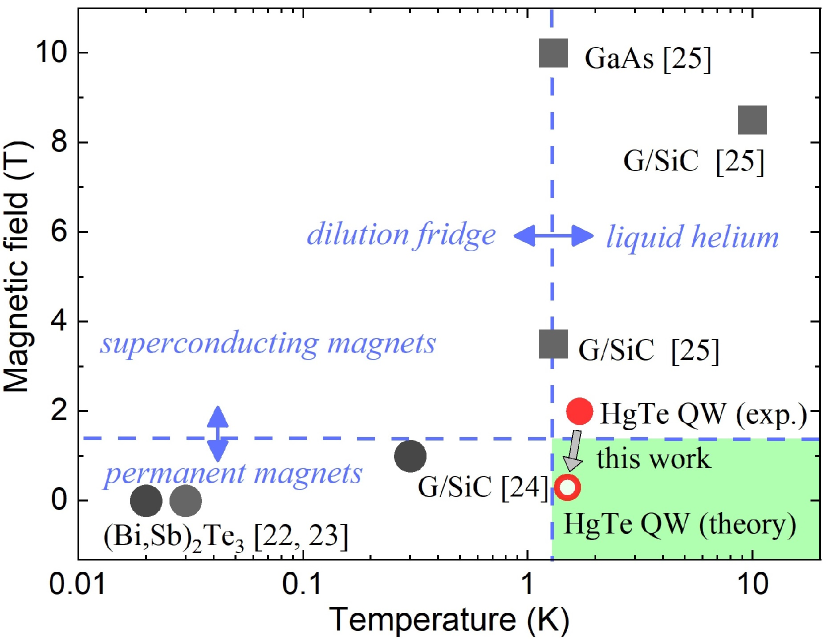
In Fig. 1 we compare performances of several quantum Hall effect (QHE) resistance standards presented as a function of magnetic field and temperature. Squares correspond to QHE standards that reached the relative precision equal or better than 10-9 based on graphene and GaAs/GaAlAs quantum wells. Circles correspond to QHE resistance standards that reached a proof of concepts stage (relative precision below than 10-9). They are based either on graphene with permanent magnets or ferromagnetic materials. The blue dotted lines mark the limit of magnetic field and temperature related technological barriers: superconducting magnets and dilution refrigerators correspondingly. For the dissemination of the resistance standards in wider markets, new standards should be developed that can operate at magnetic fields allowing the usage of permanent magnets and at temperatures allowing the use of liquid helium coolers. The green region in Fig. 1, is the only one accessible for both permanent magnets Vaimann et al. (2013) and liquid helium systems Richardson (2018).
As can be seen in Fig. 1, all currently used resistance standards operate at stringent experimental conditions: high magnetic fields B (requiring the use of superconducting coils) or extremely low temperatures T (requiring the use of dilution refrigerators), see Fig. 1. For example, typically, B = 10 T and T = 1.5 K for the GaAs-based standards. Recently, using the anomalous QHE resistance Chang et al. (2013) of a ferromagnetic topological insulator, feasibility of QHE resistance standards without applying magnetic field (B = 0 T) was demonstrated Bestwick et al. (2015); Götz et al. (2018). Additionally, QHE was observed in epitaxial graphene with 1 T permanent magnets Parmentier et al. (2016). However, both experiments required extremely low temperatures of 300 mK, provided only by dilution refrigerators. The less stringent QHE standard metrology conditions (B 3.5 T and T 1.3 K) were recently achieved in epitaxial graphene Ribeiro-Palau et al. (2015). This was enabled by the very large Landau levels (LLs) splitting related to the hosting of massless Dirac fermions by the specific graphene band structure Lafont et al. (2015); Novoselov et al. (2007). Unfortunately, suitable metrological devices were obtained only by using graphene layers deposited on SiC substrates (G/SiC), with the mobility values restricted to 104 cm2V-1 s-1, which limited metrological applications to magnetic fields higher than 3.5 T. Furthermore, because the G/SiC surface is usually covered by resists Lara-Avila et al. (2011), the device properties degrade with time Yang et al. (2016). Therefore, the quest for better standards is still ongoing.
The main motivation of this work was to overcome the graphene material challenges by using a two-dimensional material that mimics the graphene-like band structure but also shows higher carrier mobility. Another motivation was in research for a semiconductor material with well-established epitaxial fabrication and device processing techniques providing, with a high wafer yield, cost-efficient QHE resistance standard devices with identical geometry, contact quality and a long sensor lifetime.
Due to the recent progress in MBE), (Cd,Hg)Te-based QWs with a low carrier concentration and a very high carrier mobility can be grown, allowing for the observation of quantum limit = 1 conditions in magnetic fields below 1 T Kozlov et al. (2015). Additionally, QHE in HgTe QWs with graphene-like band structures was reported Büttner et al. (2011), and there structures were recently observed even at liquid nitrogen temperatures Kozlov et al. (2014); Khouri et al. (2016). These findings show that HgTe/(Cd,Hg)Te QWs are promising candidates for use in QHE metrology. In this work, we demonstrate that HgTe/(Cd,Hg)Te QWs with the thicknesses close to the dc and trivial band ordering, eliminating coexistence of conducting topological helical edge states together with QHE chiral states, allows reaching very favorable cryomagnetic conditions for the QHE resistance standards operation: low enough magnetic fields enabling use of permanent magnets (B 1.4 T) simultaneously with liquid helium coolers (teperatures of T 1.3 K) – see the green region and the circles in Fig. 1.
II RESULTS AND DISCUSSION
II.1 Investigated structures
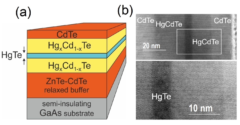
Quantum structures were grown by MBE on GaAs (013) substrates Dvoretsky et al. (2010). Three samples S1, S2 and S3, containing HgTe QWs with the thicknesses and barrier compositions of 7.1 nm, 8.0 nm, HgTe/Cd0.62Hg0.38Te, and 6.5 nm, HgTe/Cd0.65Hg0.35Te, respectively, have been studied. Measurements were performed on lithographically defined Hall bars with the dimensions of L W = 80 20 µm2, and L W = 40 20 µm2 (samples S1 and S2, respectively) and L W = 650 50 µm2 (sample S3). Additionally, samples S2 and S3 had a top gate electrode allowing for carrier density control Majewicz et al. (2010).
Figure. 2a and . 2b show the layer sequence scheme and high-resolution electron microscopy (HREM) images of the cross section of sample S1. A perfect alignment of the successive atomic layers with the well-defined HgTe QW can be seen in Fig. 2b. Such high growth quality is crucial for obtaining the appropriate carrier mobility of HgTe QWs for QHE standards and can be reached only by the MBE growth technique.
II.2 Contribution of the TI states in QHE measurements
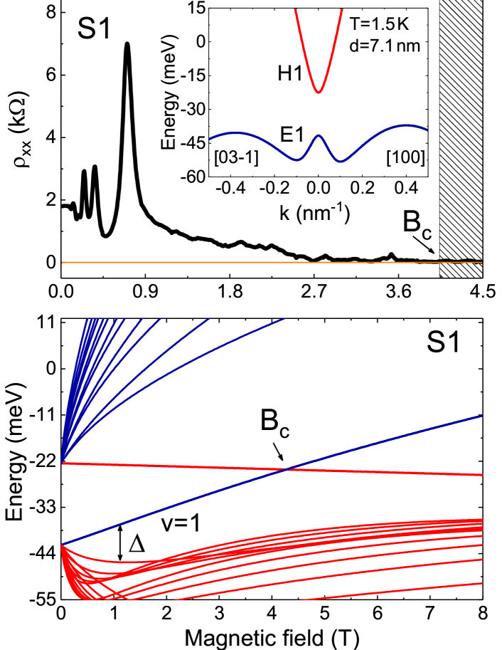
Most of the magnetotransport experiments were performed using an 8 T superconducting magnet system and standard lock-in measurement techniques. High-precision resistance measurements were performed using an HP3458A multimeter. The longitudinal and transverse resistances (B) and (B) for sample S1 are shown in Fig. 3a. The data correspond to T = 1.7 K, the hole concentration of cm-2 and mobility of 14.9 m2V-1s-1. A well-developed QHE plateau is visible already at B 0.7 T. However, the quantization is not exact, and does not go to zero.
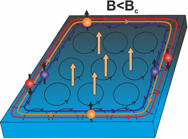
In the search for the origin of this parasitic conductivity, we consider the possibility of conduction through topological insulator 1D edge channels, as shown schematically in Fig. 4.
We calculate the band structure and LLs fan charts for samples S1 - S3 using the eight-band Hamiltonian Krishtopenko et al. (2016b), including the , and bands of bulk materials and strain effects due to lattice constant mismatch, with the parameters confirmed by our earlier investigations Kadykov et al. (2018); Marcinkiewicz et al. (2017). According to the calculation results presented in Fig. 3, sample S1 has an inverted band structure up to the critical magnetic field 4 T, at which a crossing of the highest LL from the valence band with the lowest LL from the conduction band occurs König et al. (2007, 2008); Brüne et al. (2011); Zholudev et al. (2012); Chen et al. (2012). Interestingly, tends to be zero precisely when the magnetic field approaches 4 T (see Fig. 3b). This suggests that the existence of the inverted band structure and the related topological gap are detrimental to good quantization. It is possible that the combination of both counter-propagating topological edge states and disorder promotes backscattering beyond the expected topological gap Ma et al. (2015).
To further explore conduction through the edge channels, we have investigated sample S2, which also has an inverted band structure similar to sample S1, but with a slightly larger negative energy gap. This sample was equipped with a top gate controlling the carrier type and density. Well-developed quantum resistance plateaus were observed at magnetic fields starting from above 2 T for electrons and above 5.5 T for the holes, as illustrated by a 2D map in Fig. 5a. The edge state conduction is revealed by the results of the nonlocal resistance measurements Grabecki et al. (2013) shown in the 3D plot in Fig. 5a. The value of is plotted on the logarithmic scale to better visualize the residual edge conducting channels extending to the QHE regions. As shown in Fig. 5 the resistance becomes very large when the Fermi level lies in the topological gap and decreases for magnetic fields higher than the critical value ( 6 T for sample S2). As can be seen, in spite of the nonlocal resistance has its maximum for the Fermi level close to the charge neutrality point, the nonlocality still persists far from the gap, in the QHE regions shown by the 2D map plotted above the 3D nonlocal resistance graph.
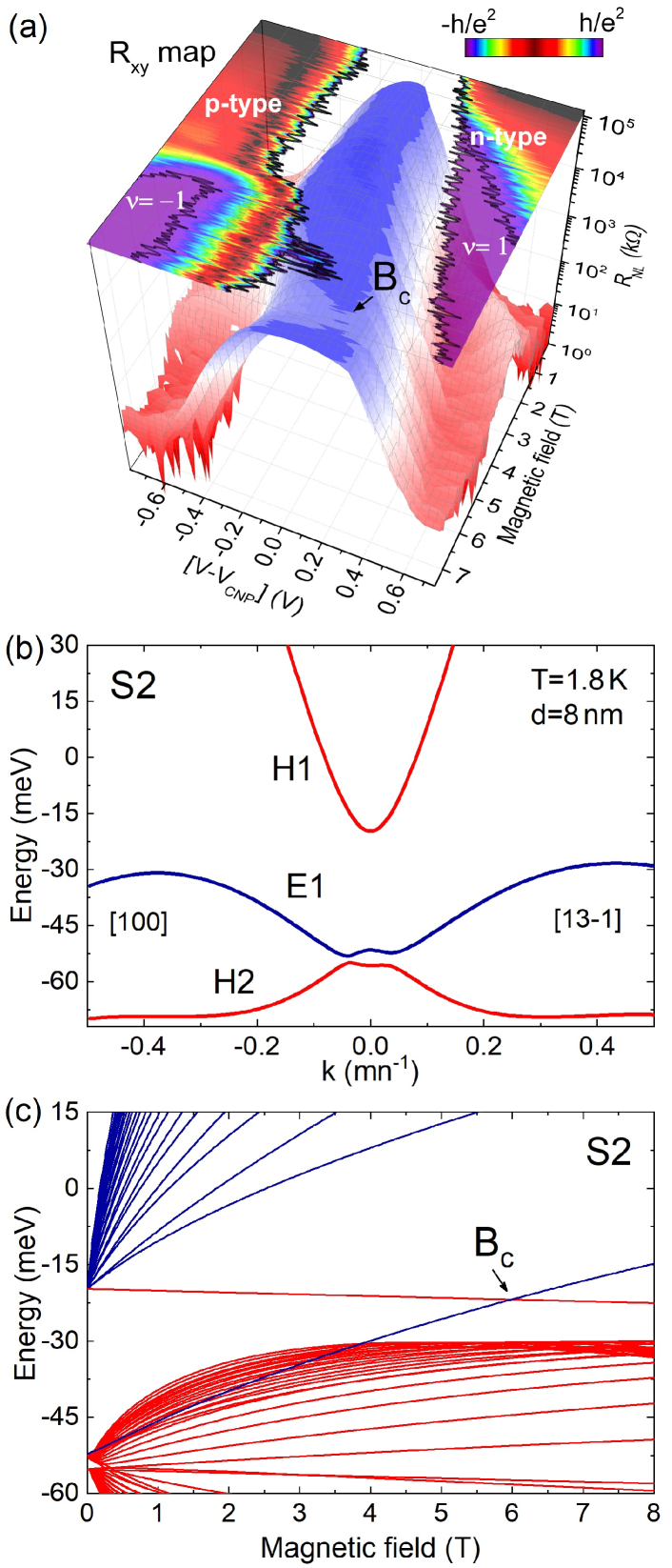
II.3 6.5 nm QW in magnetic field
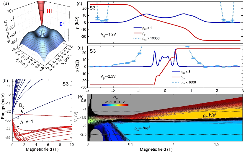
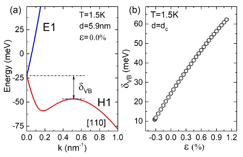
Based on results presented above, we conclude that HgTe QWs with the smallest possible should be engineered to decrease or avoid topological edge states perturbing the precision of the QHE. Figure 6 shows the band structure of sample S3. This sample has the smallest gap and the smallest critical magnetic field of the three investigated samples, 1.7 T. The magnetoresistance data for sample S3 are shown in Figure 6. On the electron side (Vg = -1.2 V, = 5 m2V-1s-1, panel c), the = 1 plateau is observed above 1.5 T. The longitudinal resistance is less than 0.1 in B = 2.5 T, and = 25,807 7 , yielding the relative accuracy in the range of .
On the hole side (Vg = -2.5 V, = 20 m2V-1s-1, panel d), the QHE is observed at a very low magnetic field B 0.5 T. However, there is a small residual contribution 20 at this field, which we attribute to the counter-propagating topological edge states. Indeed, this residual resistivity decreases with magnetic field and is finally strongly suppressed, dropping to less than 0.1 around B 2 T. Band structure calculations show that this field corresponds to the crossing of the conduction and valence band levels as well, signifying the transition from the inverted to the trivial band structure (B 1.7 T, Fig. 6b).
Figure 6e illustrate that QHE at = 1 quantum condition for p-type HgTe QWs with a width close to the take place at lower magnetic field than n-type ones. This fact and wide magnetic field region of QHE plateau for p-type we tentatively attribute to the presence of the valence band side maxima playing the role of a charge reservoir. Such a “reservoir” was also observed in G/SiC. It was proven that its existence is favourable for the formation of wide QHE plateaus Kopylov et al. (2010); Yang et al. (2016).
Summing all the values collected between 1.8 < B < 3 T at µA, we obtain . To further increase the overall precision, it would be mandatory to fabricate the QWs with non-inverted band ordering and the highest possible Fermi velocity.
II.4 Strain engineering for metrology applications
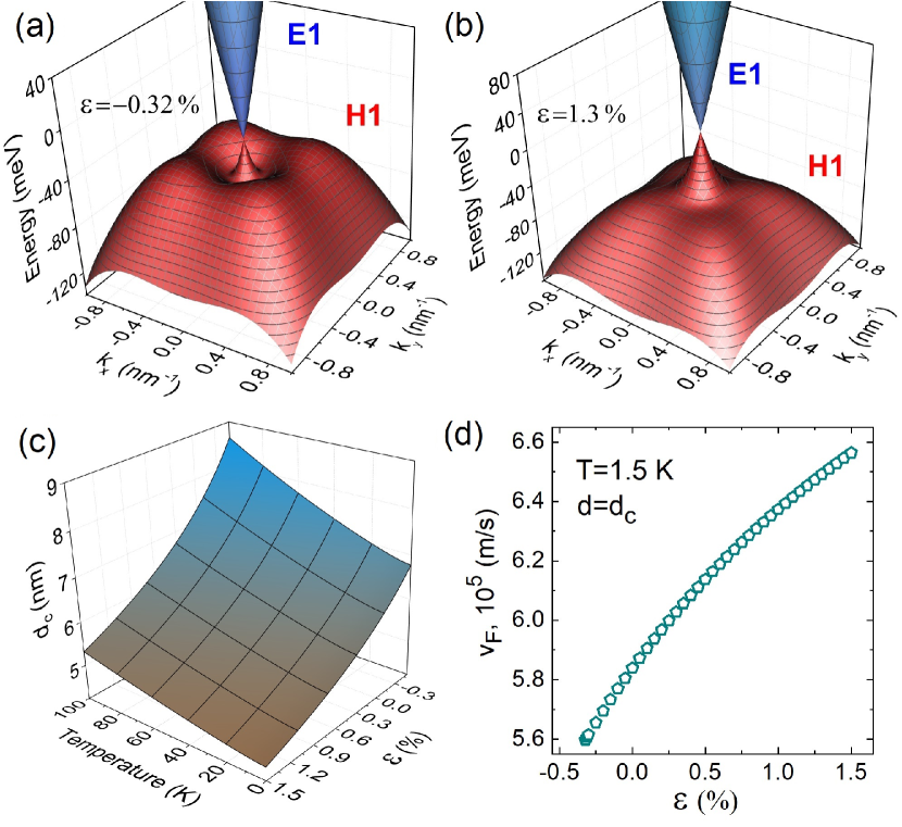
The results presented above show that good quantization precision at fields close to 0.5 T can be obtained by material engineering (slightly narrower QWs with the non-inverted band structure, 0 T). Further improvements in the QHE metrological conditions, i.e., lowering the operating magnetic field and increasing the temperature can be obtained in the QWs with higher Fermi velocity . This velocity is determined by the slope of the linear energy dispersion. Higher slope and higher , lead to increase of the energy spacings between the LLs. Recently, it has been experimentally demonstrated that the use of CdTe-Cd0.5Zn0.5Te strained-layer superlattices on GaAs as virtual substrates with an adjustable lattice constant allows effective control of the strain in the HgTe QWs from tensile ( < 0, –0.32 % for CdTe buffer) to compressive ( > 0, up to +1.40 %). Leubner et al. (2016) Following this idea, we have performed calculations of the critical width and the Fermi velocity for the QWs with 2D massless Dirac fermions ( = 0 T) at different strains and at temperatures up to 100 K. The obtained results are shown in Figure 7 for the QWs grown along the (001) direction. Krishtopenko et al. (2016b) It is worth noting that the results for the (013) QWs are qualitatively the same. It can be seen in Fig. 7 that the compressive strain indeed leads to an increase in the of the 2D massless Dirac fermions.
To illustrate the advantages of HgTe QWs as the QHE resistance standards, in Fig. 8, we compare the energy spacing between the LLs () at the quantum limit conditions ( = 1) for G/SiC, GaAs/(Al,Ga)As QWs and the investigated HgTe/(Cd,Hg)Te QWs. It is conventionally assumed that thermal excitations cease to be relevant for metrological applications for 100 , corresponding to 13 meV at T = 1.5 K. The second condition is > 1, where is the carrier mobility that determines the degree of the LL energy broadening. Both conditions, > 1 and 100 kBT, merge together, defining the metrological regions marked by arrows in Figure 8.
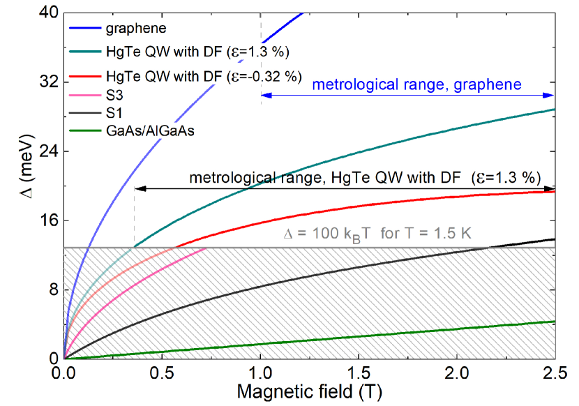
The second, the magnetic field condition, is a limiting factor for G/SiC for which the 1 m2V-1s-1 and > 1 conditions areis fulfilled only for a magnetic field B > 1 T. In HgTe QW samples, (mobility 10 m2V-1s-1) this condition is fulfilled already at 0.1 T. One can see that the metrological range for HgTe QWs samples may be obtained in relatively lower magnetic fields.
The optimum T 1.5 K metrological conditions for HgTe QWs are predicted with d = 6.4 nm ( = -0.32 %) and d = 4.6 nm ( = 1.3 %) for B 0.3 T and 0.5 T respectively. These QWs are hosting Dirac fermions with normal band ordering, ensuring maximum landau level splittings at absence of topological edge conducting channels. In Fig. 7c) we show results of calculations of the critical thickness of the HgTe QWs as a function of the strain and temperature.
III CONCLUSION
We have investigated the HgTe/(Cd,Hg)Te QWs in view of their application for new competitive QHE standards. We have shown that the coexistence of helical quantum spin Hall states and conventional chiral quantum Hall states in the topologically non-trivial region (d > , ) may restrict the accuracy of the Hall resistance quantization. At the same time, our results demonstrate that for the non-inverted QWs close to the critical width , at which Dirac fermions control the charge transport, the QHE metrological conditions can be reached for holes (p-type samples) in very favorable cryomagnetic conditions: low magnetic fields (going even below 0.5 T) and at relatively high temperatures (going even above 1.5 K). These conditions are substantially more favourable than those required for the use of current QHE standards. Our experiments and realistic band structure calculations indicate a possibility for further improvements of the QHE metrological conditions in compressively strained HgTe/(Cd,Hg)Te QWs, for which the Fermi velocity is even higher. This opens the door for the development of QHE metrological devices operating with permanent magnets (without superconducting coils) and at liquid helium temperatures (without dilution refrigerators). Accordingly, MBE-grown (Hg,Cd)Te-based QWs with Dirac fermions are semiconductor nanostructures with prospects for a large scale fabrication and a wide use of QHE resistance standards devices by academic and industrial institutions.
Acknowledgements.
The research in Poland was partially supported by the Foundation for Polish Science through the IRA Program financed by EU within SG OP Program and No. TEAM/2016-3/25, by the National Science Centre, Poland, decisions No. DEC-2011/02/A/ST3/00125, 2013/10/M/ST3/00705, UMO-2015/17/N/ST3/02314, 2016/22/E/ST7/00526 and UMO-2017/25/N/ST3/00408. The authors also acknowledge Russian Foundation for Basic Research (Grants 15-52-16008 and 16-02-00672), ARPE Terasens project and Terahertz Platform both provided by Occitanie Region. The theoretical calculations for the compressively strained QWs were performed in the framework of project 16-12-10317, supported by the Russian Science Foundation. S. S. Krishtopenko and A. Kadykov acknowledge the Russian Ministry of Education and Science (MK-1136.2017.2 and SP-5051.2018.5). The authors gratefully thank Z. D. Kvon from the Institute of Semiconductor Physics (Siberian Branch, Russian Academy of Sciences) for stimulating and fruitful discussions as well as for providing the processed gated Hall bar samples.Appendix A APPENDIX
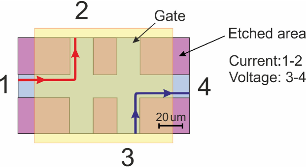
Figure 5 in the main text presents the behaviour of non-local resistance vs magnetic field and gate voltage. In conventional semiconductors, nonlocal resistance shows a well-pronounced zero, because the resistance decays exponentially with distance L between the two Hall arms according to exp, where is the sheet resistance, and W is the width of the Hall bar Van der Pauw (1958). In the experiment, was defined as the ratio between the measured voltage on 3-4 contacts and applied current 10 nA on 1-2 contacts (see Figure 9).
It should be stressed that for the samples with the band structure close to the Dirac band structure, the holes provide more favourable conditions for the QHE resistance standards, namely, lower magnetic fields and larger plateaus. The results presented in Figure 6(c-e) show an asymmetry between the QHE results for holes (panel d) and electrons (panel c). It may be observed that for holes, the QHE plateaus are wider and start at lower magnetic fields. We attribute this characteristic to the specific details of the HgTe valence band structure. The valence band side maxima play the role of a charge reservoir. Such a “reservoir” was also observed in G/SiC. It was proven that its existence is favourable for the formation of wide QHE plateaus Yang et al. (2016); Kopylov et al. (2010). Thus, a tuning of the energy difference between the position of the side maxima in the valence band and charge neutrality point (marked as , see Fig. 10) as a function of the strain in the HgTe layer is a powerful approach for controlling/adjusting the QHE plateau width. Figure 10 illustrates the implementation of the compressive strain into the system, giving rise to the increase in the and the disappearance of the side maxima.
Although we have demonstrated that HgCdTe QWs have the potential to be new competitive resistance standards, further material engineering is still necessary to obtain practical metrological QHE standards. Let us discuss briefly the most important and challenging developments. The first goal of material engineering is to further decrease the longitudinal resistance. It can also be seen that this parasitic resistance depends on the Fermi level and decreases by almost an order of magnitude, with the gate voltage changing from -2.2 V to 2.5 V. This indicates that in the metrological samples, an even better accuracy of can be obtained by playing with the relative positions of the central and side maxima Krishtopenko and Teppe (2018) as well as the doping level. Additionally, tuning of the carrier density with gates may lead to undesired current leakages, generating errors in the resistances and/or noise. Therefore, once the band structure and the optimal hole density are established, the samples for the final metrological devices should be grown and processed without the gate.
References
- Dornhaus et al. (2006) R. Dornhaus, G. Nimtz, and B. Schlicht, Narrow-gap semiconductors, Vol. 98 (Springer, 2006).
- Gałazka and Sosnowski (1967) R. R. Gałazka and L. Sosnowski, “Conduction Band Structure of Cd0.1Hg0.9Te,” Phys. Status Solidi B 20, 113 (1967).
- Orlita et al. (2014) M. Orlita, D. M. Basko, M. S. Zholudev, F. Teppe, W. Knap, V. I. Gavrilenko, N. N. Mikhailov, S. A. Dvoretskii, P. Neugebauer, and C. Faugeras, “Observation of three-dimensional massless Kane fermions in a zinc-blende crystal,” Nat. Phys. 10, 233 (2014).
- Teppe et al. (2016) F. Teppe, M. Marcinkiewicz, S. S. Krishtopenko, S. Ruffenach, C. Consejo, A. M. Kadykov, W. Desrat, D. But, W. Knap, and J. Ludwig, “Temperature-driven massless kane fermions in hgcdte crystals,” Nat. Comm. 7 (2016), 10.1038/ncomms12576.
- Dubowski et al. (1981) J. J. Dubowski, T. Dietl, W. Szymańska, and R. R. Gałazka, “Electron scattering in CdxHg1-xTe,” J. Phys. and Chem. Solids 42, 351 (1981).
- Rogalski et al. (2016) A. Rogalski, P. Martyniuk, and M. Kopytko, “Challenges of small-pixel infrared detectors: a review,” Rep. Prog. Phys. 79, 46501 (2016).
- Ruffenach et al. (2017) S. Ruffenach, A. Kadykov, V. V. Rumyantsev, J. Torres, D. Coquillat, D. But, S. S. Krishtopenko, C. Consejo, W. Knap, S. Winnerl, M. Helm, M. A. Fadeev, N. N. Mikhailov, S. A. Dvoretskii, V. I. Gavrilenko, S. V. Morozov, and F. Teppe, “Hgcdte-based heterostructures for terahertz photonics,” APL Materials 5, 035503 (2017).
- Morozov et al. (2017) S. V. Morozov, V. V. Rumyantsev, M. A. Fadeev, M. S. Zholudev, K. E. Kudryavtsev, A. V. Antonov, A. M. Kadykov, A. A. Dubinov, N. N. Mikhailov, S. A. Dvoretsky, and V. I. Gavrilenko, “Stimulated emission from hgcdte quantum well heterostructures at wavelengths up to 19.5 m,” Appl. Phys. Lett. 111, 192101 (2017).
- König et al. (2007) M. König, S. Wiedmann, C. Brüne, A. Roth, H. Buhmann, L. W. Molenkamp, X.-L. Qi, and S.-C. Zhang, “Quantum spin Hall insulator state in HgTe quantum wells,” Science 318, 766 (2007).
- König et al. (2008) M. König, H. Buhmann, L. W. Molenkamp, T. Hughes, C.-X. Liu, X.-L. Qi, and S.-C. Zhang, “The quantum spin hall effect: theory and experiment,” J. Phys. Soc. Jpn. 77, 31007 (2008).
- Brüne et al. (2011) C. Brüne, C. X. Liu, E. G. Novik, E. M. Hankiewicz, H. Buhmann, Y. L. Chen, X. L. Qi, Z. X. Shen, S. C. Zhang, and L. W. Molenkamp, “Quantum Hall effect from the topological surface states of strained bulk HgTe,” Phys. Rev. Lett. 106, 126803 (2011).
- Qi and Zhang (2011) X.-L. Qi and S.-C. Zhang, “Topological insulators and superconductors,” Reviews of Modern Physics 83, 1057 (2011).
- Roche and Valenzuela (2015) S. Roche and S. O. Valenzuela, Topological insulators: Fundamentals and perspectives (John Wiley & Sons, 2015).
- Büttner et al. (2011) B. Büttner, C. X. Liu, G. Tkachov, E. G. Novik, C. Brüne, H. Buhmann, E. M. Hankiewicz, P. Recher, B. Trauzettel, and S. C. Zhang, “Single valley Dirac fermions in zero-gap HgTe quantum wells,” Nat. Phys. 7, 418 (2011).
- Krishtopenko et al. (2016a) S. S. Krishtopenko, W. Knap, and F. Teppe, “Phase transitions in two tunnel-coupled HgTe quantum wells: Bilayer graphene analogy and beyond,” Scientific reports 6, 30755 (2016a).
- Klitzing et al. (1980) K. v. Klitzing, G. Dorda, and M. Pepper, “New method for high-accuracy determination of the fine-structure constant based on quantized Hall resistance,” Phys. Rev. Lett. 45, 494 (1980).
- Tong (2016) D. Tong, “Lectures on the quantum Hall effect,” (Department of Applied Mathematics and Theoretical Physics, Centre for Mathematical Sciences, Wilberforce Road, Cambridge 2016), arXiv:1606.06687 (2016).
- Poirier and Schopfer (2009) W. Poirier and F. Schopfer, “Resistance metrology based on the quantum Hall effect,” Eur. Phys. J. Spec. Top 172, 207 (2009).
- Jeckelmann and Jeanneret (2001) B. Jeckelmann and B. Jeanneret, “The quantum Hall effect as an electrical resistance standard,” Rep. Prog. Phys. 64, 1603 (2001).
- Taylor and Witt (1989) B. N. Taylor and T. J. Witt, “New international electrical reference standards based on the Josephson and quantum Hall effects,” Metrologia 26, 47 (1989).
- Vaimann et al. (2013) T. Vaimann, A. Kallaste, A. Kilk, and A. Belahcen, in 2013 Africon (2013) pp. 1–5.
- Richardson (2018) R. Richardson, Experimental Techniques In Condensed Matter Physics At Low Temperatures (CRC Press, 2018).
- Chang et al. (2013) C.-Z. Chang, J. Zhang, X. Feng, J. Shen, Z. Zhang, M. Guo, K. Li, Y. Ou, P. Wei, and L.-L. Wang, “Experimental observation of the quantum anomalous Hall effect in a magnetic topological insulator,” Science 340, 167 (2013).
- Bestwick et al. (2015) A. J. Bestwick, E. J. Fox, X. Kou, L. Pan, K. L. Wang, and D. Goldhaber-Gordon, “Precise quantization of the anomalous hall effect near zero magnetic field,” Phys. Rev. Lett. 114, 187201 (2015).
- Götz et al. (2018) M. Götz, K. M. Fijalkowski, E. Pesel, M. Hartl, S. Schreyeck, M. Winnerlein, S. Grauer, H. Scherer, K. Brunner, C. Gould, F. J. Ahlers, and L. W. Molenkamp, “Precision measurement of the quantized anomalous hall resistance at zero magnetic field,” Applied Physics Letters 112, 072102 (2018).
- Parmentier et al. (2016) F. D. Parmentier, T. Cazimajou, Y. Sekine, H. Hibino, H. Irie, D. C. Glattli, N. Kumada, and P. Roulleau, “Quantum Hall effect in epitaxial graphene with permanent magnets,” Sci. Rep. 6, 38393 (2016).
- Ribeiro-Palau et al. (2015) R. Ribeiro-Palau, F. Lafont, J. Brun-Picard, D. Kazazis, A. Michon, F. Cheynis, O. Couturaud, C. Consejo, B. Jouault, and W. Poirier, “Quantum Hall resistance standard in graphene devices under relaxed experimental conditions,” Nat. Nanotechnol 10, 965 (2015).
- Lafont et al. (2015) F. Lafont, R. Ribeiro-Palau, D. Kazazis, A. Michon, O. Couturaud, C. Consejo, T. Chassagne, M. Zielinski, M. Portail, and B. Jouault, “Quantum Hall resistance standards from graphene grown by chemical vapour deposition on silicon carbide,” Nat. Commun 6, 6806 (2015).
- Novoselov et al. (2007) K. S. Novoselov, Z. Jiang, Y. Zhang, S. V. Morozov, H. L. Stormer, U. Zeitler, J. C. Maan, G. S. Boebinger, P. Kim, and A. K. Geim, “Room-temperature quantum Hall effect in graphene,” Science 315, 1379 (2007).
- Lara-Avila et al. (2011) S. Lara-Avila, K. Moth-Poulsen, R. Yakimova, T. Bjørnholm, V. Fal’ko, A. Tzalenchuk, and S. Kubatkin, “Non-Volatile Photochemical Gating of an Epitaxial Graphene/Polymer Heterostructure,” Adv. Mater 23, 878 (2011).
- Yang et al. (2016) M. Yang, O. Couturaud, W. Desrat, C. Consejo, D. Kazazis, R. Yakimova, M. Syväjärvi, M. Goiran, J. Béard, P. Frings, M. Pierre, A. Cresti, W. Escoffier, and B. Jouault, “Puddle-induced resistance oscillations in the breakdown of the graphene quantum hall effect,” Phys. Rev. Lett. 117, 237702 (2016).
- Kozlov et al. (2015) D. A. Kozlov, Z. D. Kvon, N. N. Mikhailov, and S. A. Dvoretskii, “Quantum hall effect in a system of gapless Dirac fermions in HgTe quantum wells,” JETP Lett 100, 724 (2015).
- Kozlov et al. (2014) D. A. Kozlov, Z. D. Kvon, N. N. Mikhailov, S. A. Dvoretskii, S. Weishäupl, Y. Krupko, and J.-C. Portal, “Quantum Hall effect in HgTe quantum wells at nitrogen temperatures,” Appl. Phys. Lett 105, 132102 (2014).
- Khouri et al. (2016) T. Khouri, M. Bendias, P. Leubner, C. Brüne, H. Buhmann, L. W. Molenkamp, U. Zeitler, N. E. Hussey, and S. Wiedmann, “High-temperature quantum Hall effect in finite gapped HgTe quantum wells,” Phys. Rev. B 93, 125308 (2016).
- Dvoretsky et al. (2010) S. Dvoretsky, N. Mikhailov, Y. Sidorov, V. Shvets, S. Danilov, B. Wittman, and S. Ganichev, “Growth of HgTe quantum wells for IR to THz detectors,” J. Elec. Materi. 39, 918 (2010).
- Majewicz et al. (2010) G. M. Majewicz, D. Śnieżek, T. Wojciechowski, E. Baran, P. Nowicki, T. Wojtowicz, and J. Wróbel, “Low temperature processing of nanostructures based on II - IV semiconductors quantum wells,” Acta Phys. Pol. 126, 1174 (2010).
- Krishtopenko et al. (2016b) S. S. Krishtopenko, I. Yahniuk, D. B. But, V. I. Gavrilenko, W. Knap, and F. Teppe, “Pressure- and temperature-driven phase transitions in hgte quantum wells,” Phys. Rev. B 94, 245402 (2016b).
- Kadykov et al. (2018) A. Kadykov, S. Krishtopenko, B. Jouault, W. Desrat, W. Knap, S. Ruffenach, C. Consejo, J. Torres, S. Morozov, N. Mikhailov, S. Dvoretskii, and F. Teppe, “Temperature-Induced Topological Phase Transition in HgTe Quantum Wells,” Phys. Rev. Lett. 120, 86401 (2018).
- Marcinkiewicz et al. (2017) M. Marcinkiewicz, S. Ruffenach, S. S. Krishtopenko, A. M. Kadykov, C. Consejo, D. B. But, W. Desrat, W. Knap, J. Torres, A. V. Ikonnikov, K. E. Spirin, S. V. Morozov, V. I. Gavrilenko, N. N. Mikhailov, S. A. Dvoretskii, and F. Teppe, “Temperature-driven single-valley dirac fermions in hgte quantum wells,” Phys. Rev. B 96, 035405 (2017).
- Zholudev et al. (2012) M. Zholudev, F. Teppe, M. Orlita, C. Consejo, J. Torres, N. Dyakonova, M. Czapkiewicz, J. Wróbel, G. Grabecki, N. Mikhailov, S. Dvoretskii, A. Ikonnikov, K. Spirin, V. Aleshkin, V. Gavrilenko, and W. Knap, “Magnetospectroscopy of two-dimensional hgte-based topological insulators around the critical thickness,” Phys. Rev. B 86, 205420 (2012).
- Chen et al. (2012) J.-C. Chen, J. Wang, and Q.-F. Sun, “Effect of magnetic field on electron transport in HgTe/CdTe quantum wells: Numerical analysis,” Phys. Rev. B 85, 125401 (2012).
- Ma et al. (2015) E. Y. Ma, M. R. Calvo, J. Wang, B. Lian, M. Mühlbauer, C. Brüne, Y.-T. Cui, K. Lai, W. Kundhikanjana, Y. Yang, M. Baenninger, M. König, C. Ames, H. Buhmann, P. Leubner, L. W. Molenkamp, S.-C. Zhang, D. Goldhaber-Gordon, M. A. Kelly, and Z.-X. Shen, “Unexpected edge conduction in mercury telluride quantum wells under broken time-reversal symmetry,” Nat. Comm. 6, 7252 (2015).
- Grabecki et al. (2013) G. Grabecki, J. Wróbel, M. Czapkiewicz, Ł. Cywiński, S. Gierałtowska, E. Guziewicz, M. Zholudev, V. Gavrilenko, N. N. Mikhailov, S. A. Dvoretski, F. Teppe, W. Knap, and T. Dietl, “Nonlocal resistance and its fluctuations in microstructures of band-inverted HgTe/(Hg,Cd)Te quantum wells,” Phys.Rev. B 88, 165309 (2013).
- Kopylov et al. (2010) S. Kopylov, A. Tzalenchuk, S. Kubatkin, and V. I. Fal’ko, “Charge transfer between epitaxial graphene and silicon carbide,” Appl. Phys. Lett. 97, 112109 (2010).
- Leubner et al. (2016) P. Leubner, L. Lunczer, C. Brüne, H. Buhmann, and L. W. Molenkamp, “Strain Engineering of the Band Gap of HgTe Quantum Wells Using Superlattice Virtual Substrates,” Phys. Rev. Lett. 117, 86403 (2016).
- Van der Pauw (1958) L. J. Van der Pauw, “A method of measuring the resistivity and Hall coefficient on lamellae of arbitrary shape,” Philips Tech.l Rev. 20, 220 (1958).
- Krishtopenko and Teppe (2018) S. S. Krishtopenko and F. Teppe, “Realistic picture of helical edge states in HgTe quantum wells,” Physi. Rev. B 97, 165408 (2018).