Quantum Annealing Machines Based on Semiconductor Nanostructures
Abstract
The development of quantum annealing machines (QAMs) based on superconducting qubits has progressed greatly in recent years and these machines are now widely used in both academia and commerce. On the other hand, QAMs based on semiconductor nanostructures such as quantum dots (QDs) appear to be still at the initial elementary research stage because of difficulty in controlling interaction between qubits. In this paper, we review a QAM based on a semiconductor nanostructures such as floating gates (FGs) or QDs from the viewpoint of the integration of qubits. We theoretically propose the use of conventional high-density memories such as NAND flash memories for the QAM rather than construction of a semiconductor qubit system from scratch. A large qubit system will be obtainable as a natural extension of the miniaturization of commercial-grade electronics, although further effort will likely be required to achieve high-quality qubits.
I Introduction
Since the commercial success of D-Wave’s superconducting machines Dwave ; Dwave2 , development of the quantum annealing machines (QAMs) has been one of the hottest topics in science and technology. The theoretical background can be traced back to Nishimori’s work in the 1990s Nishimori ; Finnila . The progress of research on QAMs has also stimulated new investigations on annealing methods based on digital computers Yamaoka ; Fujitsu . QAMs are expected to solve the combinatorial optimization algorithms of NP-hardness problems in a shorter time than classical annealing methods. Solvers of this type are required for artificial intelligence (AI), whose progress is a momentous trend and expected to bring about drastic change in society. Faster solving of combinatorial optimization problems by QAMs has the potential to lead to more efficient development of AI algorithms. QAMs have also been used recently to investigate the quantum Boltzmann machineDumoulin ; Kieferova ; Benedetti .
Many combinatorial problems, including the traveling salesman problem, can be mapped to the problems to find ground states of the Ising Hamiltonian, expressed by Lucas ; MAXCUT ; Kahruman
| (1) |
where the variable is a classical bit of two values(). The first term is the interaction term with a coupling constant , and the second term is the Zeeman energy with an applied magnetic field . In the case of a QAM Dickson ; Boixo1 ; Boixo2 ; Bermeister ; IonTrap , a tunneling term is added and expressed by
| (2) |
where the variables are expressed by Pauli matrices () instead of digital bits. The tunneling term is controlled such that it disappears at the end of the calculation. Thus, and initially and and finally. Although the Hamiltonian (2) can be found in many physical systems in nature, the tunneling term and the Ising term should be controlled separately and locally by electric gates to realize QAMs.
The advantage of superconducting qubits lies in the long coherence time of superconducting states Dwave . Compared with the advance of superconducting qubits, the development of semiconductor qubits seems slower Ladd . In semiconductor systems, spin and charge degrees of freedom can provide the qubit mechanism. A qubit using spin is called a spin qubit and that using charge is called a charge qubit book . Spin qubits have longer coherence time because their independence from the noisy environment is greater than that of charge qubits. For a realistic machine, it is crucially important to have a sufficient number of qubits. Although two spin qubits are sufficiently controlled Veldhorst ; Maune ; Kawakami , the qubit operations more than three and more qubits have not yet been well succeeded because the difficulty of controlling qubit-qubit interactions. The greatest advantage of using semiconductor devices is the possibility that the smallest artificial structures at the highest density can be manufactured in factories. However, the spin qubits have not yet relished this benefit. We think that charge qubits Hayashi ; Shinkai ; Gorman ; Ward ; NEC ; Valiev ; Brandes ; Fujisawa ; Petta ; Zhang ; Shi ; Mark are better than spin qubits from the viewpoint of an integration of qubits, because charge qubits are interacting with mutual Coulomb interaction through capacitive couplings. Thus, although charge qubits have generally less coherence time than spin qubits, here we rather consider a charge qubit system by reviewing the proposal of a QAM using the conventional NAND flash memory consisting of floating gate (FG) cells in Ref. tanamotoQAM , and we extend the structure of a qubit to a coupled quantum dot (QD) system. Coherent control of charge qubits using semiconductor QDs has been demonstrated in Ref. Hayashi , and coherent dynamics of two qubits based on coupled quantum dots (CQDs) has enabled two-qubit operations in Ref. Shinkai . Silicon charge-qubit operation has been experimentally shown in Ref. Gorman using a single-electron effect. New types of coupling in charge qubits have been experimentally investigated in Ref. Ward . The smaller the semiconductor devices becomes, the larger the quantized energy intervals are expected to become, which is expected to result in increased coherence. The fact that the fabrication technologies for semiconductor devices continue to progress is also beneficial to charge qubits.
Now, the cell size of advanced 2D NAND flash memory Masuoka ; Samsung ; Toshiba is less than 15 nm iedm2012 ; iedm2013 , and the transistor size are entering into the quantum region below 7 nmTSMC7nm ; Samsung7nm ; IBM7nm . The disadvantage of the charge qubit’s short coherence time is expected to be reduced as transistor size decreases. There are two important points that 2D NAND flash memory can be used as a good candidate of the charge qubit system. First, in flash memory with 15 nm cells, single-electron effects can be observed at room temperature Nicosia . The second point is that the inevitable interence effects between FG cells can be used as the interaction between qubits. In commercial 2D NAND flash memories Toshiba ; Samsung ; iedm2013 ; iedm2012 the distance between FG cells is of the same order as the size of the FG cells. Thus, interference effects between FG cells are a major issue in present NAND flash memories Lee . In order to reduce the interference between FG cells, air-gap technologies are used iedm2013 because the dielectric constant of air is smaller than that of tunneling oxide such as SiO2 (which has a dielectric constant of 3.8).
NAND flash memories have a dominant share of the growing market for storage applications extending from mobile phones to data storage devices in data centers Takeuchi . The NAND flash memories have the advantages of high-density memory capacity and low production cost per bit with low power consumption and high-speed programming and erasing mechanisms. Now data storage of personal computers is also transitioning from hard disk to flash memory. An FG cell corresponds to 1 bit for a single-level cell and bits for a multi-level cell. Each FG is typically made of highly doped polysilicon and placed in the middle of a gate insulator of a transistor Brown ; Aritome . If there is no extra charge in an FG, the cell behaves like a normal transistor. In the programming or writing step, electrons are injected into the FG by applying voltage to the control gate. In the erasing step, electrons are ejected from the FG to the substrate by applying voltage to the back gate. The amount of the charges of the FG determines the threshold voltage above which the current between the source and drain changes. In NAND flash memories, the FG cells are connected like a NAND gate circuit. In general, the distance between the FGs is of the same order as the size of the FG, realizing a high-density memory. For example, Sako et al. developed 64 Gbit NAND flash memory in 15 nm CMOS technology Toshiba , which is organized by a unit of 16 KB bit-lines 128 word-lines. This means that the number of closely arrayed FG cells in a single unit is 16KB 128 2 MB. The integration and miniaturization of flash memory cells have progressed continuously and the current flash memories have stacked 3D structures using trapping layers Samsung2 ; Toshiba2 .
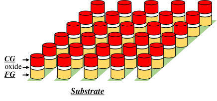
First, we theoretically show that a two-dimensional (2D) FG array can be used as a QAM. The QAM proposed here has the structure shown in Fig.1. The FG cells are capacitively connected to each other, which is the same arrangement as that in a commercial flash memory. The fundamental idea is that we will be able to regard a small FG cell in the single-electron region as a charge qubit. The size of the current FG NAND flash memory is 15 nm iedm2012 ; iedm2013 , but it can be shrunk to less than 7 nmTSMC7nm ; Samsung7nm ; IBM7nm . When the doping concentration of electrons is cm-3, the number of electrons in a volume of 101030 nm3 is about 15 and countable. Once we can control the single-electron effects, we can realize a two-level system by using a crossover region between two different quantum states with different numbers of electrons, following, for example, Ref. Makhlin .
Even when we can use state-of-the-art fabrication technologies, it is still difficult to control charge qubits with perfect coherence. In general quantum computations, accurate control of wave functions is required from initial states to final states for measurements. On the contrary, in a QAM, the condition of the strict control of wave functions can be loosened provided that the final state is an eigenfunction of the target Hamiltonian, and the intermediate processes can include disturbance with several kinds of noise. Thus, in the application of a QAM, there will be the advantages of small semiconductor devices such as high integration and productivity.
In Ref tanamotoQAM , we have shown that the FG array in 2D NAND flash memories can constitute a QAM by using the capacitive coupling between neighboring cells. In this setup, the physical interactions are limited to the neighboring qubits. On the other hand, in order to solve general combinatorial problems, the connection of all qubits to any qubits (all-to-all connection) should be prepared. There are two major methods of realizing all-to-all connection based on solid-state qubits that have interactions only between neighboring qubits. The Minor Embedding (ME) method by Choi ME1 ; ME2 is used for the ”Chimera” graph structure in the D-wave machine where logical qubits are replaced by chains of physical qubits. Lechner, Hauke, and Zoller (LHZ) LHZ proposed an alternative embedding method in which pairs of logical spins correspond to physical spins. T. Albash et al reported that the ME method showed better performance Albash2 , although the possibility remains that the LHZ method will be improved in the future. In this paper, we mainly consider how to implement the ME method in a 2D charge qubit array.
The remainder of this paper is organized as follows: In Sec. II, we briefly review the derivation of the Ising Hamiltonian from an FG array. In Sec. III, we explain how a QAM is implemented using CQD array. In Sec. IV, we discuss how to realize all-to-all connection in the semiconductor qubits. In Sec. V, we briefly discuss the effects of noise and decoherence on our QAM. We close with a summary and conclusions in Sec. VI.
II General formalism of Ising interactions
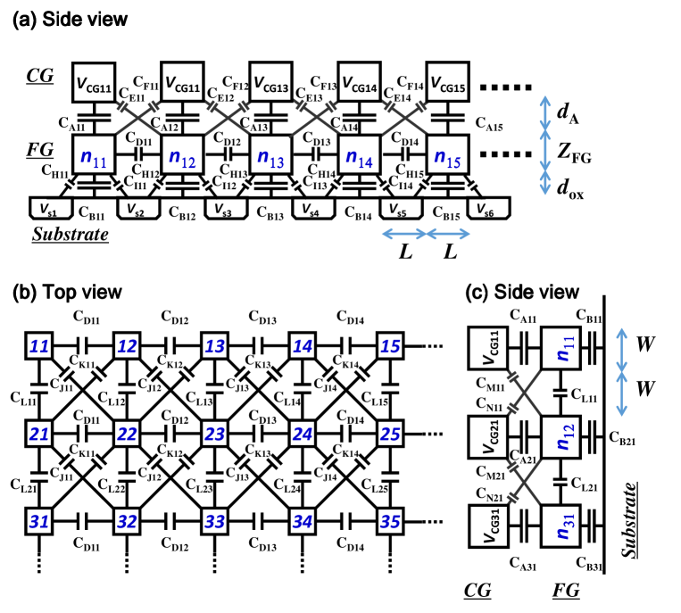
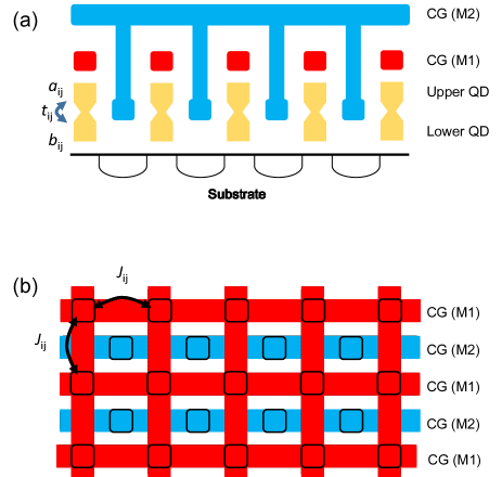
Here, we derive an Ising Hamiltonian from the coupled 2D FG array by using a capacitance network model Pavan as shown in Fig. 2. Each cell consists of an FG and a control gate. We assume a Coulomb blockade regime and the number of electrons of the FG cell at position is expressed by . We can also define charge states . FGs are capacitively connected to the nearest FG, CG, and substrate with source and drain. The Ising interaction comes from charging energy. The charging energy of the 2D system of Fig. 2 is given by
where ,…, are stored charges on capacitances. The charge distribution is obtained after minimizing by adjusting the Lagrange multipliers . When we neglect the interaction beyond the next-neighboring interactions, after the simple but long calculations, the charge distribution is obtained and given by
| (3) |
where
| (4) | |||||
| (5) | |||||
| (6) | |||||
| (7) | |||||
| (8) | |||||
| (9) | |||||
| (10) | |||||
| (11) | |||||
| (12) | |||||
with
| (13) | |||||
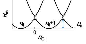
Here, we have continuously completed the squares to find the minimum points of the charging energy. Concretely, starting from , we take and so on. Note that s in Eq. (4) include , , and . Thus, the form of Eq. (3) generates the Ising interactions between neighboring FG cells through Eq. (5). And thus, the Ising interactions and Zeeman terms are obtained as a result of the parabolic form of the charging energy. Following Ref .Makhlin , the superposition state is constructed around the region
| (14) |
This is the region where the charging energy of electrons equals that of the electrons, and quantum states and states can be defined as shown in Fig. 3. We use the effective gate voltage given by
| (15) |
(). For this region, we can approximate the following equation
| (16) |
where , are Pauli matrix and unit matrix, respectively, based on the system.
Thus, the charging energy term as a function of transforms to
| (17) |
where the Ising interactions are given by
| (18) | |||||
| (19) | |||||
| (20) | |||||
| (21) |
The magnetic field is given by
| (22) | |||||
and
| (23) | |||||
| (24) | |||||
| (25) |
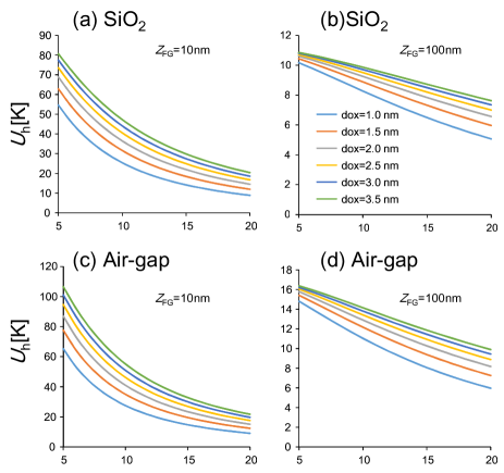
Thus, the 2D FG array can be mapped to a 2D Ising spin system with antiferromagnetic couplings. In this 2D case, there are next-nearest couplings by and . These next-nearest couplings induce spin states conflict with those induced by nearest neighboring couplings. We can erase the next-nearest couplings by inserting the air-gap iedm2013 in the middle of four FG cells. This is because the dielectric constant of air is lower than that of SiO2, we can reduce the effect of the capacitance couplings. In Ref. tanamotoQAM , numerical estimations based on 1D capacitance network model were carried out. Those calculations showed that the smaller size of FGs induces higher temperature operations as expected. In Ref. tanamotoQAM , Technology CAD(TCAD) tools were also used and it was shown that the response speed of the FGs are in order of 10-11 s for nm FGs. Here, let us check the effect of the next-nearest coupling by calculating the , which corresponds to the height of the charging energy and is calculated by the coefficient of in Eq.(22) such as
| (26) | |||||
Figure 4 shows an example of the numerical calculations of surrounded by qubits when the coupling ratio is given by 0.3. The coupling ratio indicates the degree of controllability of the gate electrode. and given by
| (27) |
as it is frequently used in the field of FG memory. We consider a FG whose size and width have the same value, . When the thickness of the tunneling oxide is , the thickness of the insulator between the FG and the CG is given by
| (28) |
The capacitances are defined by using their simplest expressions given by
| (29) | |||||
| (30) | |||||
| (32) |
where and F/m. For the case of the air-gap in the middle of the four qubits, we use
| (33) |
Figure 4 shows that weak next-nearest interactions, which corresponds to the air-gap cases ((c)(d)), enhance the single electron effects, compared with the existence of full next-nearest interactions of the SiO2 cases ((a)(b)). From Fig. 4, 3%-30% increase in can be seen for nm and 20%-50% increase in can be seen for nm.
As long as the capacitance network model is used, , and other physical parameters depend on only capacitances. In semiconductor systems, however, the capacitance changes depending on applied voltages. As an example, the capacitance of PN junction changes depending on the change of the depletion region as the applied voltage changes Grove . In the present structure, the NAND flash memory includes many different regions of n-type and p-type semiconductors. Thus, it is possible that the capacitances change complicatedly when the applied bias is changed. The detailed dependence of the change of capacitances will be estimated by carrying out TCAD simulations. This will require a lot of calculations and considerations, and be future issues.
II.1 Analytical formation of tunneling term
The tunneling term Eq. (2) is derived by using the Wentzel-Kramers-Brillouin (WKB) approximation Harrison , and given by
| (34) | |||||
where 3.0 eV is the potential height of the tunneling barrier, and are the effective masses of electrons in Si and tunneling barrier, respectively (is an electron mass in vacuum). and c are annihilation operators of both sides of the tunneling barrier. is the wave vector at the Fermi energy. nm is the Bohr radius and eV is the Rydberg constant. and are the numbers of electrons on the two sides of the tunneling barrier that participate in the tunneling event. This tunneling term is a function of the gate voltage depending on the shift in Fermi energy , such as , and is calculated from the FG doping concentration. When increases, the effective tunneling barrier is lowered and the tunneling rate increases (switches on). Conversely, when decreases, the effective tunneling barrier is raised and the tunneling switches off. Thus, the tunneling can be switched on or off by controlling the gate and substrate bias. Eq. (34) is the expression of the tunneling from the approach of many electrons. The smaller the number of electrons in FGs becomes, the better coherence of qubits is expected. Thus, in such case of a smaller number of electrons, we will have to construct more elaborate formulation in the future.
III QAM based on CQD
As mentioned in the introduction, because it is very difficult to uniformly construct small structures of nm scale, a simpler structure is better for fabrication processes. In this meaning, NAND flash memory is best for QAM from the viewpoint of its simple structure. Here, we consider a QAM of a little bit more complicated structure based on coupled quantum dots (CQDs). CQDs or double QDs have been widely investigated in the field of nano-physics JPSJ1 ; JPSJ2 ; JPSJ3 ; JPSJ4 ; Nishiguchi ; tana2 . Depending on whether an extra electron exists in one QD or the other QD, the logical states and are defined. Because we are focusing on the integration of qubits, we have to stack QDs as shown in Fig. 5. If we don’t have to switch on/off the tunneling between two QDs, we can stack the simple oxide material such as SiO2 between two QDs. However, because quantum annealing process requires switching on/off of the tunneling between QDs, we need the structure that enables the switching on/off of the tunneling. In the usual lateral QDs JPSJ4 , two positions of the excess electron is usually connected by ”split-gates”. The split-gates change the depth of the depletion layer and the tunnelings between QDs are controlled. In the present case, we will have to embed the additional electrodes which work as the split-gate between CQDs as shown in Fig. 5. The difference from Ref. tana0 is that there are electrodes between the CQDs. Compared with a quantum computer, we do not have to switch tunneling on/off independently in the case of quantum annealer. Thus we can set a common electrode to the split-gates to switch the tunneling on/off simultaneously. For the CQDs, excess electrons are confined in the closed two QDs and the two QDs are separated from electrodes, it is expected that the coherence time of CQD system becomes larger than that of QAM based on flash memory. However, in the CQD system, we have to add additional split-gates, and the size between CQDs (qubits) becomes larger. These are considered to degrade the coherence. In the future, we will have to estimated these trade-off between QAMs based on flash memory and CQDs.
III.1 Hamiltonian of CQDs
Here we consider the Hamiltonian of the 2D arrayed CQDs by starting from the tunneling Hamiltonian
| (35) |
where describes the annihilation operator when the excess electron exists in the upper (lower) QD, and shows the electronic energy of the upper (lower) QD. is the number of CQDs. Compared with the case of FG system Eq.(34), we could describe the electronic system more microscopically. is the charging energy of the CQD system. Because we consider the Coulomb blockade in the weak coupling region, the operational temperature be less than the charging energies. The operational speed should be less than the CR constant of the capacitance network so that the double-well potential profile generated by the charging energy is effective adiabatic region. As for the interaction between qubits, the distribution of the extra charge is considered to be antiferromagnetic because of the repulsive Coulomb interaction. Similarly to the FG case, we showed that this interaction between qubits is an Ising interaction by minimizing a similar charging energy in Ref. tana0 ; tana1 . Thus, the Hamiltonian of the CQD system is given by
| (36) | |||||
IV Toward all-to-all connection
For connecting all qubits to any qubits, i.e., all-to-all connection, the two major methods are well known: the Minor embedding method by Choi ME1 ; ME2 and the method by LHZ LHZ . Let us discuss how to realize these methods in the NAND flash memory system.
IV.1 Implementation of the minor embedding
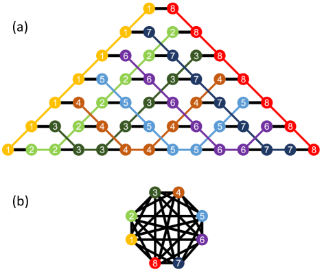
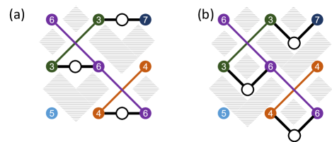
Figure 6 shows the ME method of Ref. ME1 ; ME2 . Circles indicate qubits and solid lines indicate interactions between qubits. In order to connect a spin with any distant spins, Choi ME1 ; ME2 introduced a logical spin that consists of many spins with the same spin states. In Fig. 6, the qubits with the same number constitute a logical qubit. The logical qubits are connected by strong interactions. In Ref. ME1 , the condition of the strength of the interaction in the qubits of a logical state (-th tree) is expressed by
| (37) |
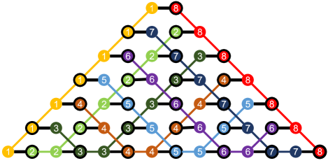
This means that coupling in the logical spins () is stronger than the sum of the surrounding coupling plus the local magnetic field . Note that the interactions between logical qubits in Refs. ME1 ; ME2 are ferromagnetic interactions. On the other hand, the interactions described in the previous sections are antiferromagnetic interactions. We consider that similar discussions as in Refs. ME1 ; ME2 are possible. Because the ground state of a 1-D Ising antiferromagnetic chain is given by , we can apply this idea to the antiferromagnetic system as shown in Fig. 7.
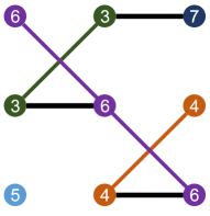
Let us consider the implementation of the minor embedding(ME) method to the 2D Ising array with constant antiferromagnetic interactions using nano structures. In the ME method, we have to prepare three types of bonding between two qubits as shown in Fig. 8: (i) The first type is a fixed coupling between qubits as shown in Eq.(37). (ii) The second type is that there is no interaction between two qubits. (iii) The third type is that the coupling represents the data and should be changeable. Here, we consider possible forms of these types of bonding, focusing on the 2D qubit array with Coulomb interactions through insulating materials. Then, the constant interaction of the first type is already realizable through the insulating material with relatively high dielectric constant such as SiO2.
The second type is realizable by replacing the materials between the qubits with ones that have low dielectric constants. In the case of Si-based qubits, the air-gap iedm2013 that means the space between two qubits is filled with air is available to present interaction between the qubits. The third type can be realized by inserting a new qubit that controls the strength of the bonding by using the method proposed in Ref. Niskanen . It is considered that, by applying large oscillating bias, the magnitude of the interaction between the two qubits is controlled as shown in Ref. Niskanen . Figures 9 (a) and (b) illustrate these proposals. The shaded parts indicate the air-gap region where space is filled with air or the materials with low dielectric constants. In Fig 9(b), the intermediate qubits in the controlling bonds are placed in the same lattice structure with other qubits. This structure is applicable to the CQD system mentioned in Sec.2, because the split-gate electrodes are inserted in the middle of the four qubits.
IV.2 Application of LHZ method
The LHZ method also enables connection of all qubits to any qubits LHZ . In the LHZ method, logical Ising spins are encoded in physical qubits with constraints. Each physical qubit represents the relative configuration of two logical spins such that the physical qubit takes the value 1 if the two connected logical spins point in the same direction and 0 otherwise. New constraints are introduced as four-body interactions or three body interactions to keep the consistency of qubit configurations. Because the four-body interaction and three-body interaction are unnatural interactions, we have to generate this higher order interactions starting from natural two-body interactions. Lechner showed that the four-body interaction can be realized by using a series of CNOT gates Lechner . In order to realize the series of CNOT gates, sufficient quantum coherence will be required. Thus this method requires perfect control of the electronic system.
V Decoherence
In Ref. tana0 and Ref. tanamotoQAM , we roughly estimated the coherence time of the charge qubit based on the spin-boson model Legget . In Ref. tana0 and Ref. tanamotoQAM , we considered a low-temperature region, where only acoustic phonons play a major role in the decoherence mechanism. The interaction term between a qubit and acoustic phonons is derived from that of amorphous SiO2 Garcia ; Wurger . The estimated coherences are given by around 4.8 s, during which more than thousands of quantum calculations can be realized if the switching time is less than nano seconds. However, these estimations were carried out on the assumption that electrons are controlled perfectly. Thus, in the current realistic situation, the controllability of countable electrons by electrodes would be the first issue to be addressed in the experiments.
VI Conclusion
We have reviewed prospects for the QAM based on semiconductor nano-structures from the viewpoint of the integration of qubits. In order to increase the coherence of qubits, the separation of qubits from their environment is important. On the other hand, separation of qubits from their environment leads to weak control of the qubits. Thus, there is a trade-off in the relationship between qubit system with their environments, and here we focus on the charge qubit from the viewpoint of their natural mutual capacitive couplings. In addition, it is considered that an integration of qubits is more difficult than integration of conventional CMOS transistors, in particular when the qubit structure is quite different from conventional commercial semiconductor devices. Thus, the fastest way, which also means the most economical way, is to use the current fabrication technologies to build a qubit system. Accordingly, we have proposed a charge-qubit system using NAND flash memory. We also proposed similar qubit system based on a CQD system. Because fabrication lines in the factory already exist, we hope business judgment will proceed experiments for testing our proposals.
Acknowledgments
We thank T. Hiraoka, T. Hioki, T. Marukame, H. Goto, M. Hayashi, K. Kuboki and T. Otsuka for discussions.
References
- (1) M. W. Johnson et al.,Nature 473, 194 (2011).
- (2) T. Lanting, et al., Phys. Rev. X 4, 021041 (2014).
- (3) T. Kadowaki and H. Nishimori, Phys. Rev. E 58, 5355 (1998).
- (4) A.B. Finnila, M.A. Gomez, C. Sebenik, C. Stenson, and J.D. Doll, Chem. Phys. Lett. 219, 343 (1994).
- (5) M. Yamaoka, C. Yoshimura, M. Hayashi, T. Okuyama, H. Aoki, and H. Mizuno, 2015 IEEE Int. Solid State Circuits Conference (ISSCC), 24.3 (2015).
- (6) M. Aramon, G. Rosenberg, E. Valiante, T. Miyazawa, H. Tamura, and H. G. Katzgraber, ArXiv:1806.08815.
- (7) V. Dumoulin, I.J. Goodfellow, A. Courville, and Y. Bengio AAAI’14 Proceedings of the Twenty-Eighth AAAI Conference on Artificial Intelligence Pages 1199-1205 (2014).
- (8) M. Kieferová and N. Wiebe Phys. Rev. A 96, 062327 (2017).
- (9) M. Benedetti, J. Realpe-Gómez, R. Biswas, and A. Perdomo-Ortiz Phys. Rev. X 7, 041052 (2017).
- (10) A. Lucas, Front. Phys. 2, 5 (2014).
- (11) S. Sousa, Y. Haxhimusa, and W.G. Kropatsch, Int. Workshop on Graph-Based Representations in Pattern Recognition GbRPR 2013, 244 (2013).
- (12) S. Kahruman et al., Int. J. of Computational Science and Engineering, 3, 211 (2007).
- (13) N.G. Dickson et al., Nat. Commun. 4, 1903 (2013).
- (14) S. Boixo, T. Albash, F.M. Spedalieri, N. Chancellor, and D.A. Lidar, Nat. Commun. 4, 3067 (2013).
- (15) S. Boixo, T.F. Ronnow, S.V. Isakov, Z. Wang, D. Wecker, D.A. Lidar, J.M. Martinis, and M. Troyer, Nat. Phys. 10, 218 (2014).
- (16) A. Bermeister, D. Keith, and D. Culcer, Appl. Phys. Lett. 105, 192102 (2014).
- (17) T. Gra, D. Ravento, B. Juliá-Díaz, C. Gogolin, and M. Lewenstein, Nat. Commun. 7, 11524 (2016).
- (18) T.D. Ladd, F. Jelezko, R. Laflamme, Y. Nakamura, C. Monroe, and J.L. ÓBrien, Nature 464, 45 (2010).
- (19) ”Scalable quantum computers: Paving the way to realization” (2001/2 S.L. Braunstein, and H.K. Lo, Wiley-VCH.
- (20) M. Veldhorst et al., Nature 526, 410 (2015).
- (21) B.M. Maune et al., Nature 481, 344 (2012).
- (22) E. Kawakami et al., Nature Nanotechnol. 9, 666 (2014).
- (23) T. Hayashi, T. Fujisawa, H. D. Cheong, Y. H. Jeong, and Y. Hirayama, Phys. Rev. Lett. 91, 226804 (2003).
- (24) G. Shinkai, T. Hayashi, T. Ota, and T. Fujisawa, Phys. Rev. Lett. 103, 056802, (2009).
- (25) J. Gorman, D. G. Hasko, and D. A. Williams, Phys. Rev. Lett. 95, 090502 (2005).
- (26) D. R. Ward, D. Kim, D. E. Savage, M. G. Lagally, R. H. Foote, M. Friesen, S. N. Coppersmith, and M. A. Eriksson, npj Quantum Inf 2 16032 (2016).
- (27) T. Yamamoto, Y. A. Pashkin, O. Astafiev, Y. Nakamura and J. S. Tsai, Nature 425, 941 (2003).
- (28) L. Fedichkin, M. Yanchenko, and K. A. Valiev, Nanotechnology 11, 387 (2000).
- (29) T. Brandes and T. Vorrath, Phys. Rev. B 66, 075341 (2002).
- (30) T. Fujisawa, T. Hayashi, H.D. Cheong, Y.H. Jeong, and Y. Hirayama, Physica E 21 1046 (2004).
- (31) J. R. Petta, A. C. Johnson, C. M. Marcus, M. P. Hanson, and A. C. Gossard, Phys. Rev. Lett. 93, 186802 (2004).
- (32) M. W. Y. Tu and W.M. Zhang, Phys. Rev. B 78, 235311 (2008).
- (33) Z. Shi, C. B. Simmons, D. R. Ward, J. R. Prance, R. T. Mohr, T. S. Koh, J. K. Gamble, X. Wu, D. E. Savage, M. G. Lagally, M. Friesen, S. N. Coppersmith, and M. A. Eriksson, Phys. Rev. B 88, 075416 (2013).
- (34) M. Friesen, J. Ghosh, M. A. Eriksson, and S. N. Coppersmith, Nat. Communications 8 15923 (2017).
- (35) T. Tanamoto, Y. Higashi, and J. Deguchi arXiv:1706.07565, to appear in J. Appl. Phys.
- (36) F. Masuoka, M. Momodomi, Y. Iwata, and R. Shirota, 1987 Int. Electron Devices Meeting (IEDM), 552 (1987).
- (37) M. Sako et al., 2015 IEEE Int. Solid State Circuits Conference (ISSCC), 7.1 (2015).
- (38) D. Kang et al., 2016 IEEE Int. Solid State Circuits Conference (ISSCC), 7.1 (2016).
- (39) J. Seo et al., 2013 IEEE Int. Electron Devices Meeting (IEDM), 76 (2013).
- (40) A. Goda and K. Para, 2012 IEEE Int. Electron Devices Meeting (IEDM), 13 (2012).
- (41) J. Chang et al., 2017 IEEE Int. Solid State Circuits Conference (ISSCC), 12.1 (2017).
- (42) T. Song et al., 2017 IEEE Int. Solid State Circuits Conference (ISSCC), 12.2 (2017).
- (43) T. Nogami et al., 2017 IEEE Symp. VLSI Tech. 148 (2017).
- (44) G. Nicosia et al., IEEE Int. Electron Devices Meeting (IEDM), 378 (2015).
- (45) J. D. Lee, S. H. Hur, and J.D. Choi, IEEE Electron Device Letters 23, 264 (2002).
- (46) K. Takeuchi, T. Hatanaka, and S Tanakamaru, IEICE Electronics Press, 9, 779 (2012).
- (47) Nonvolatile Semiconductor Memory Technology: A Comprehensive Guide to Understanding and Using NVSM Devices, edited by W.D. Brown and Joe Brewer, (publisher Wiley-IEEE Press, New York, 1997).
- (48) S. Aritome, 2000 IEEE Int. Electron Devices Meeting (IEDM), 763 (2000).
- (49) C. Kim et al., 2017 IEEE Int. Solid State Circuits Conference (ISSCC), 11.4 (2017).
- (50) R. Yamashita et al., 2017 IEEE Int. Solid State Circuits Conference (ISSCC), 11.1 (2017).
- (51) Y. Makhlin, G. Schön, and A. Shnirman, Rev. Mod. Phys. 73, 357 (2001).
- (52) V. Choi, Quant. Inf. Proc. 7, 193 (2008).
- (53) V. Choi, Quant. Inf. Proc. 10, 343 (2011).
- (54) W. Lechner, P. Hauke, and P. Zoller, Sci. Adv. 1, e1500838 (2015).
- (55) T. Albash, W. Vinci, and D. A. Lidar, Phys. Rev. A 94, 022327 (2016).
- (56) P. Pavan, L. Larcher, and A. Marmiroli, “Floating Gate Devices: Operation and Compact Modeling”, (Kluwer, Boston, 2004).
- (57) A. S. Grove, “Physics and Technology of Semiconductor Devices”, (Wiley, New York, 1967).
- (58) W. A. Harrison, Phys. Rev. 123, 85 (1961).
- (59) T. Fujii, and K. Ueda, J. Phys. Soc. Jpn. 74, 127 (2005).
- (60) A. Rosch, J. Paaske, J. Kroha, and P. Wölfle, J. Phys. Soc. Jpn. 74, 118 (2005).
- (61) M. Eto, J. Phys. Soc. Jpn. 74, 95 (2005).
- (62) A. Oiwa, T. Fujita, H Kiyama, G. Allison, A. Ludwig, A. D. Wieck, and S. Tarucha, J. Phys. Soc. Jpn. 86, 011008(2017).
- (63) K. Nishiguchi and A. Fujiwara, IEEE Int. Electron Devices Meeting (IEDM), 791 (2007).
- (64) T. Tanamoto and K. Muraoka, Appl. Phys. Lett. 96, 022105 (2010).
- (65) T. Tanamoto, Phys. Rev. A 61, 022305 (2000).
- (66) T. Tanamoto, Phys. Rev. A 64, 062306 (2001).
- (67) A. O. Niskanen, Y. Nakamura, and J.S. Tsai, Phys. Rev. B 73, 094506 (2006). IEEE Trans. Electron Devices, 61, 2802 (2014).
- (68) A.J. Leggett, S. Chakravarty, A.T. Dorsey, and M.P. A. Fisher, A. Garg, and W. Zwerger, Rev. Mod. Phys. 59, 1 (1987).
- (69) A. J. Garćia and J. Fernández, Phys. Rev. B 55, 5546 (1997).
- (70) A. Würger, Europhys. Lett. 28, 597 (1994).
- (71) W. Lechner, arXiv:1802.01157v2.