Atomistic tight binding study of quantum confined Stark effect in GaBixAs1-x/GaAs quantum wells
Abstract
Recently, there has been tremendous research interest in novel bismide semiconductor materials (such as GaBixAs1-x) for wavelength-engineered, low-loss optoelectronic devices. We report a study of the quantum confined Stark effect (QCSE) computed for GaBixAs1-x/GaAs quantum well (QW) structures based on large-scale atomistic tight-binding calculations. A comprehensive investigation of the QCSE as a function of the applied electric field orientations and the QW Bi fractions reveals unconventional character of the Stark shift at low Bi compositions (=3.125%). This atypical QCSE is attributed to a strong confinement of the ground-state hole wave functions due to the presence of Bi clusters. At technologically-relevant large Bi fractions ( 10%), the impact of Bi clustering on the electronic structure is found to be weak, leading to a quadratic Stark shift of the ground-state transition wavelength, similar to previously observed in other conventional III-V materials. Our results provide useful insights for the understanding of the electric field dependence of the electronic and optical properties of GaBixAs1-x/GaAs QWs, and will be important for the design of devices in the optoelectronics and spintronics areas of research.
1 Introduction
Quantum confined Stark effect (QCSE), which is defined as the impact of an electric field on the optoelectronic properties of nanostructures such as quantum wells (QWs) and quantum dots (QDs), has been extensively studied for a wide range of material systems Kuo_Nature_2005 ; Empedocles_Science_1997 ; Krenner_PRL_2005 ; Nakaoka_PRB_2006 . In the presence of an external electrical field, the confined charge carriers (electrons and holes) feel a force which pushes the corresponding wave functions in the opposite directions. This causes a spatial separation between the charge carriers leading to the formation of an electric dipole. The QCSE plays an important role in the design of various photo-absorption and photo-emission devices such as electro-absorption modulators (EAMs), photovoltaics, and photo-diodes where the electric field mediated charge separation underpins the operation of the devices. For the conventional III-V semiconductor quantum wells such as made up of InGaAs/GaAs or InGaAs/InP materials, the QCSE leads to a quadratic red shift in the optical transition energies and wavelengths. Recently unconventional QCSE was reported for GaN/AlN quantum dots Nakaoka_PRB_2006 , where the application of an electric field introduced a blue shift of the optical transition wavelength. The unconventional QCSE was also reported for semiconductor quantum rings exhibiting linear or quadratic shifts depending on the direction of the applied electric fields Sousa_PRB_2017 . This work, for the first time, investigates the character of the QCSE for GaBixAs1-x/GaAs quantum well structures and reports a peculiar character of the QCSE at low Bi fractions (), where the quadratic red shift changes to linear red shift depending on the applied electric field magnitudes. Moreover, this character is found to be highly sensitive to the spatial distribution of the Bi atoms within the QW region. The detailed large-scale atomistic simulations attribute the unconventional nature of the QCSE to a strong spatial confinement of hole wave functions. By varying both and the orientation of the applied electric fields, our results indicate that the QCSE switches to a conventional quadratic red shift when the Bi fraction is increased above 10%, which is technologically relevant for devices working at the telecomm wavelengths. The presented results offer an in-depth understanding of the QCSE for GaBixAs1-x/GaAs quantum wells that will not only contribute to advance our knowledge on an important area of research where no prior theoretical study exists, but also provide a reliable guidance for the ongoing experimental efforts towards application of bismide alloys in the design of novel optoelectronic devices with significantly improved performance and suppressed loss mechanisms.
Alloying the conventional III-V semiconductors such as GaAs or InAs with a dilute fraction of bismuth (Bi) () leads to a novel class of alloys known as bismides Bismuth_containing_compounds_2013 . One of the most widely studied bismide alloy, GaBixAs1-x , has shown several unique properties such as a large band-gap reduction ( 90 meV/%Bi) with increasing Janotti_PRB_2002 ; Zhang_PRB_2005 ; Batool_JAP_2012 ; Usman_PRB_2011 , a strong spin orbit coupling Broderick_SST_2012 ; Marko_SSMS_2014 , a cross-over between the band-gap energy (Eg) and the spin split-off energy () for 12% Batool_JAP_2012 ; Usman_PRB_2011 ; Usman_PRB_2013 , and a strong confinement of the hole wave functions due to Bi pairs and clusters Usman_APL_2014 ; Usman_PRB_2013 ; Usman_PRM_2018 . These promising characteristics of the GaBixAs1-x material have opened new avenues for optoelectronic devices and sparked a tremendous experimental interest Richards_JCG_2015 ; Balanta_JoL_2017 ; Mazur_JoL_2017 ; Aziz_APL_2017 ; Makhloufi_NRL_2014 ; Marko_SR_2016 ; Balanta_JPD_2016 ; Patil_Nanotechnology_2017 . For instance, the large band-gap engineering as a function of provides opportunities to design optoelectronic devices operating in near to mid-infrared wavelengths Usman_PRA_2018 . The crossover between the band-gap energy and the spin split-off energy (E) is expected to significantly suppress CHSH Auger loss mechanisms – the dominant source of internal losses in semiconductor laser devices Broderick_SST_2012 . The strong spin orbit coupling has been proposed to offer benefits for spintronic applications Mazzucato_APL_2013 . Therefore, a comprehensive understanding of the electronic structure of bismide nanostructures in response to the applied electric fields is highly desirable for the emerging optoelectronic technologies.
The application of an electric field shifts electron and hole wave functions confined in nanostructures such as QWs or QDs in opposite directions reducing their spatial overlap. The tilting of the conduction and valence band edges due to the application of potential from the electric fields leads to a decrease(increase) in the confined electron(hole) energies, inducing a red shift in the optical transition wavelength. This effect has been observed in many conventional III-V QWs and QDs, both experimentally and theoretically. Despite tremendous ongoing experimental interests and significant relevance for optoelectronic technologies, to-date, there has been no study of the QCSE for GaBixAs1-x/GaAs QWs. In this work, we have applied a well-established and extensively bench-marked large-scale atomistic tight-binding theory to investigate the QCSE in GaBixAs1-x/GaAs QWs as a function of both electric field orientations and Bi fractions. Our calculations revealed that at low Bi fractions (=3.125%), the QCSE exhibits unconventional character. Upon a detailed study of the confined electron and hole charge densities and their electric field dependent shifts, we attributed the atypical character of the QCSE to a very strong confinement of hole states, which require large magnitude of the electric fields to shift. Somewhat surprisingly, at large Bi fractions 13% where the ground-state transition wavelength is close to 1300 nm, the QCSE exhibits a symmetric quadratic red shift in the optical transition wavelength. This is because the presence of a large number of Bi atoms leads to a relatively uniform strain profile inside the QW region and hence the hole wave functions are more uniformly spread within the QW. Our calculations report that at =13%, the ground-state optical transition wavelength is red shifted by 22 nm for a 40 kV/cm variation in the magnitude of the applied electric field, irrespective of its orientation.
2 Methods
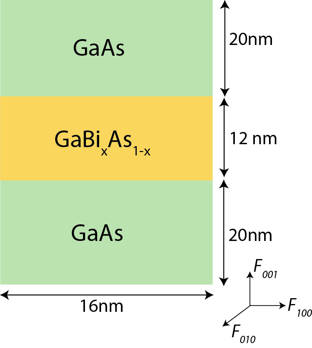
QW Geometry Parameters: A schematic diagram of the investigated quantum well structure is provided in the Fig. S1 of the supplementary material section. A single GaBixAs1-x quantum well with 12 nm width along the (001) direction and 20 nm lateral dimensions along the in-plane ((100) and (010)) directions is placed in GaAs material. The quantum well region consists of 196608 atoms, whereas the total size of the surrounding GaAs box is 20 nm 20 nm 52 nm, consisting of 851968 atoms. The boundary conditions for the simulation domain are periodic in all three spatial directions. The size of the GaAs box was selected to be sufficiently large to enable proper strain relaxation of atoms and to ensure negligible inter-well couplings along the (001) growth direction. The Bi fractions () of the QW structure are selected as 3.125%, 6.5%, 10%, and 13%, which correspond to 3072, 6389, 9831, and 12778 number of Bi atoms, respectively, randomly replacing the arsenic (As) atoms in the QW region. To investigate the effect of the lateral size of QW region, we increase the number of atoms in the QW region to 1.33 million and find that the lateral size effect on the electron and hole confinement wave functions is negligibly small. We also investigate five different random configurations to study the effect of the placement of Bi atoms as will be discussed in a later section. The ground state transition energy (GSTE) is computed from the difference between the lowest electron (e1) and the highest hole (h1) energies, and the ground state transition wavelength (GSTW) in the units of nm is defined as: GSTW = 1240/GSTE.
Strain and Electronic Structure: The lattice mismatch between the GaAs and GaBixAs1-x materials leads to strain in the crystal. We compute the strain from an atomistic valence force field (VFF) method Keating_PR_1966 by properly relaxing the crystal structure. The electronic structure calculations are performed by solving a nearest-neighbor sp3s∗ tight-binding Hamiltonian, including spin-orbit coupling. The parameters used to model GaAs and GaBi band structures were published in our previous study Usman_PRB_2011 . We note that our sp3s∗ tight-binding parameters reproduce the GaBi band structure very accurately around the point, however the high energy conduction bands do not quantitatively match the published band structure, in particular along the to X direction of the Brillouin zone. This is related to the limitation of the sp3s∗ parametrisation as discussed in the previous studies Klimeck_SM_2000 ; Sawamura_OME_2018 . However, for the GaBiAs material which is a direct band-gap material, the fitted sp3s∗ tight-binding parameters provide a very good description of the band structure properties. The model has been extensively benchmarked against a number of experimental studies on both bulk GaBixAs1-x materials Usman_PRB_2011 ; Usman_PRB_2013 and GaBixAs1-x/GaAs QWs Usman_PRM_2018 ; Broderick_PRB_2014 ; Broderick_SST_2015 . Subsequently, the tight-binding model has also shown good agreement with the experimental data sets Donmez_SST_2015 ; Balanta_JoL_2017 ; Zhang_JAP_2018 ; Dybala_APL_2017 ; Collar_AIPA_2017 ; Broderick_PRB_2014 as well as with the DFT calculations reported in the literature Kudrawiec_JAP_2014 ; Polak_SST_2015 ; Bannow_PRB_2016 .
The ground state electron and hole energies and wave functions at the point are computed for each Bi fraction in the quantum well region. The details of the VFF relaxation and tight-binding model parameters are published in our earlier work Usman_PRB_2011 . The charge density plots shown in figures 3 and 4 are plotted as follows:
| (1) | |||||
| (2) |
where and are the ground-state electron and hole wave functions corresponding to e1 and h1 energies respectively. The denotes the (001) plane. Note that in this work, charge density on anions is shown, however the charge density on cations exhibits similar trends and omitted for simplicity Usman_APL_2014 . The computation of optical transition strengths includes charge densities on both cations and anions. The simulations are performed using NanoElectronic MOdeling (NEMO-3D) tool Klimeck_IEEETED_2007_2 .
Impact of Electric Field: To study the QCSE, we investigate the effect of a static electric field whose magnitude is varied between -40 kV/cm and 40 kV/cm and the orientation of electric field is selected along the three primary crystal directions: (100), (010), and (001). The impact of electric field on electronic structure is computed by including a net potential in the diagonal part of the tight-binding Hamiltonian Usman_IOPNanotech_2011 . We note here that the theoretical investigation of the QCSE for semiconductor nanostructures has a long history, with initial studies based on variational methods Miller_PRL_1984 ; Miller_PRB_1985 and perturbation approach Lengyel_IEEE_1990 . Recently, detailed atomistic techniques have been applied towards the computation of the QCSE Usman_IOPNanotech_2011 ; Sukkabot_2018 . In this work, we have employed an atomistic tight-binding theory which is particularly well-suited to investigate the electronic structure of the highly-mismatched alloys such as GaBixAs1-x Usman_PRB_2011 .
3 Results and Discussions
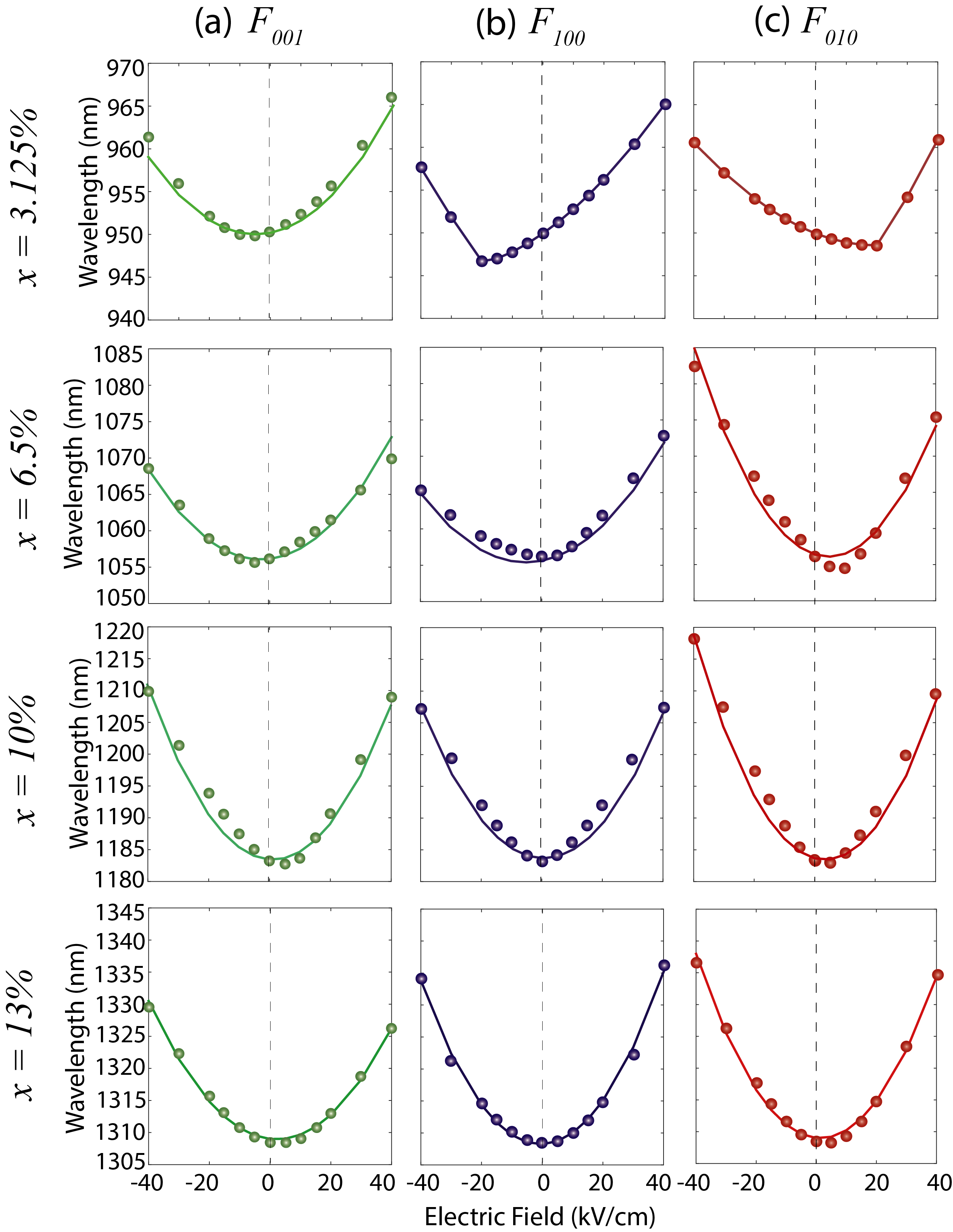
Electric Field Dependence of GSTW: Figure 1 shows the GSTW plots as a function of the applied electric fields for various Bi fractions (rows) and the three orientations of the applied electric field (columns). The application of electric field along the growth or confinement direction () leads to a conventional Stark effect irrespective of the QW Bi fraction. The GSTW red shifts when the magnitude of the electric field increases. For a net variation of 40 kV/cm in , we computed a change of approximately 22 nm, 12 nm, 25 nm, and 22 nm in the GSTW for = 3.125%, 6.5%, 10%, and 13%, respectively. It is noted that the minimum value of the GSTW is not at zero electric field, which indicates that the charge carriers are not symmetrically confined in the QW region at zero electric field. It will be shown later that this asymmetry is primarily related to the asymmetric confinement of the hole wave functions, as the electron wave functions are nearly symmetrically confined along the (001) direction.
For the in-plane electric field orientations ( and ), the plots of the GSTW at =3.125% showed a remarkable asymmetry with respect to the magnitude of the applied electric fields. The computed electric field dependent change in the GSTW is quadratic for -20 kV/cm 40 kV/cm and -40 kV/cm 20 kV/cm, and it is linear for -40 -20 kV/cm and 20 40 kV/cm. In the next few sections, we will provide a detailed analysis of this atypical GSTW character by carefully analysing the electric field dependent electron and hole energies and charge density plots. Here we note that when the Bi fraction in the QW region is increased, the QCSE becomes increasingly quadratic as have been widely reported for the conventional III-V alloys. At =13%, the dependence of the QCSE on the applied electric field is completely quadratic and exhibits approximately 21 nm and 24 nm variations in the GSTW for the applied range of the and electric fields, respectively. These variations are similar to the 22 nm change in wave length for , indicating that at =13%, the QCSE is symmetric with respect to the orientation of the applied electric field.
| Electric Field Orientation | Electric Field Orientation | Electric Field Orientation | ||||||||||
| (%) | E | (10-6) | (10-6) | R2 | E | (10-6) | (10-6) | R2 | E | (10-6) | (10-6) | R2 |
| 3.125 | 1.3127 | -91.6 | -17.1 | 0.985 | 1.3053† | -300† | -4† | 0.999† | 1.3053† | 200† | -4† | 0.999† |
| – | – | – | – | 1.3258‡ | 800‡ | 0‡ | 1.0‡ | 1.3243‡ | -800‡ | 0‡ | 1.0‡ | |
| 6.5 | 1.1735 | -39.8 | -8.9 | 0.986 | 1.1734 | -90.7 | -8.79 | 0.988 | 1.1735 | 143.2 | -15.6 | 0.982 |
| 10 | 1.0468 | 35.2 | -14 | 0.992 | 1.04647 | -43.8 | -12.7 | 0.991 | 1.0462 | 110.06 | -16.2 | 0.989 |
| 13 | 0.9473 | 41.9 | -8.5 | 0.998 | 0.9476 | -11.7 | -11.7 | 0.998 | 0.9475 | 31.7 | -12.03 | 0.996 |
Built-in Dipole Moment and Polarizability: To provide quantitative estimates of the changes in the band gap energies as a function of the applied electric fields, we fitted the GSTE, corresponding to the GSTW plots in Fig. 1, to a quadratic equation of the form:
| (3) |
where E is the value of the GSTE in the units of eV computed without the application of electric field (=0), is the orientation of the applied electric field, is the permanent dipole moment in the units of eV.cm/kV, and is a measure of the polarizability of the electron and hole wave functions in the units of eV.cm2/kV2. This equation has been widely used in the literature to investigate the electric-field-dependent shift in the GSTE Robinson_APL_2005 ; Seufert_APL_2001 . The character of the GSTE shift is dependent on many factors, including the size of the nanostructures and the material properties. For example, it has been shown that the InGaN quantum dots exhibit a Stark effect which includes both linear and quadratic components Robinson_APL_2005 ; however, the Stark shift for the CdSe quantum dots shows only a quadratic dependence on the electric field Seufert_APL_2001 . Here, we fit the equation 3 to the computed GSTE data and show that in the case of the GaBixAs1-x quantum wells, the Stark effect includes both linear and quadratic components.
Table 1 provides the fitted values of E, and for the investigated Bi fractions and the applied electric field orientations. In each case, we have also provided values, which indicate the quality of the fit of equation 1 to the GSTE plots. An value of 1.0 implies a perfect fit, indicating that the GSTE dependence on the electric field is completely represented by the quadratic formula of the equation 1. The values in the Table 1 show a general trend that for the studied GaBixAs1-x/GaAs QWs, the value of increases as increases. This suggests that at larger Bi fractions, an increasingly conventional behaviour of the QCSE is computed. For =3.125%, there was not a single fit to the computed GSTE as the dependence on the in-plane electric fields ( and ) varies between the linear and quadratic functions. Therefore, two separate fits were performed as indicated in the table by symbols and .
From the table 1, we find that the values of are larger at the small Bi fraction (=3.125%) and they generally decrease as increases. This indicates that the electron and hole wave functions are relatively largely separated at =3.125%, which gives rise to a higher built-in permanent dipole moment. This will become clearer in the later sections when we will discuss the charge density plots where the hole charge density plots show a highly confined character.
The values of , which is the measure of polarizability or the electric field response, increase when the Bi fraction in the QW region increases. This shows that at higher Bi fractions, the applied electric field has stronger impact on pulling the electron and hole charge carriers in the opposite directions, compared to the low Bi fractions. Therefore, a relatively large reduction in the spatial overlap between the electron and hole wave functions is expected for the QWs with Bi fractions above 10%, which are technologically relevant Sweeney_JAP_2013 .
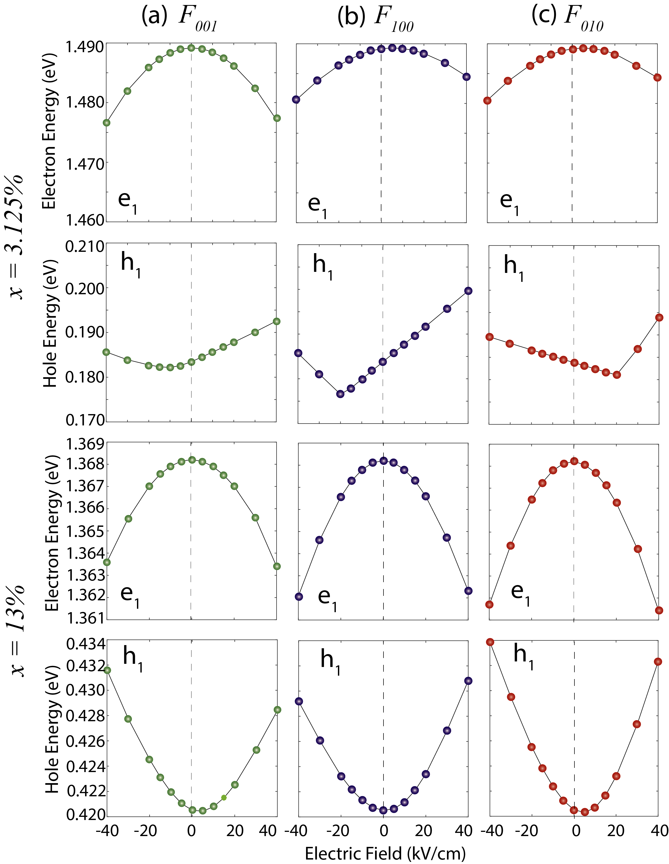
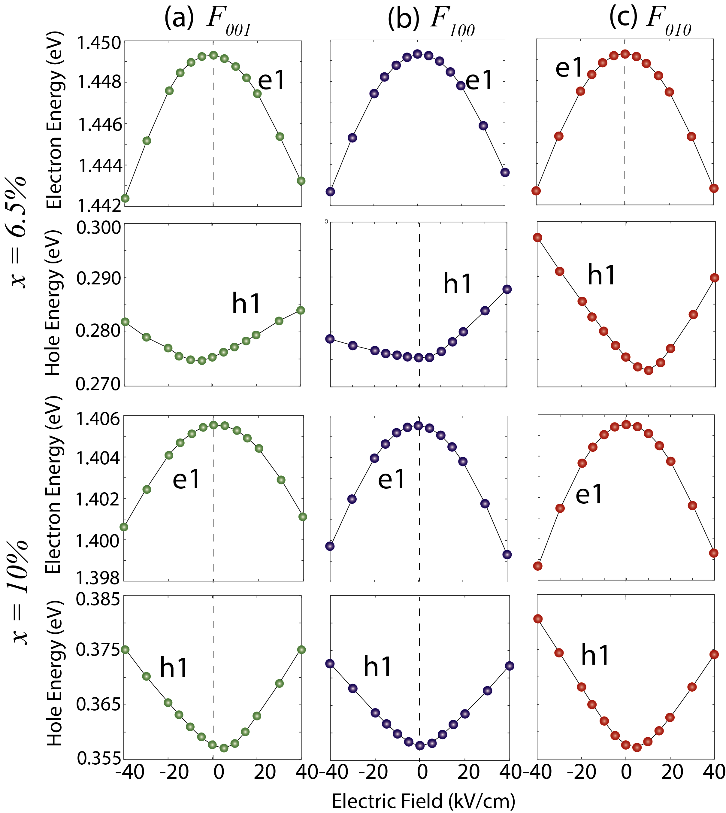
Unconventional Stark Shift of Holes Energies: To further investigate the previously discussed unconventional character of the QCSE computed for =3.125%, we plot the lowest electron (e1) and the highest hole (h1) energies as a function of the applied electric fields in Fig. 2. For comparison, we have also plotted the same energies for =13%. The corresponding plots for =6.5% and 10% are provided in Fig. S2 of the supplementary material section for reference. From these plots, it is clearly evident that the lowest electron energies (e1) exhibit a conventional quadratic dependence on the magnitude of electric fields, irrespective of the filed orientations and Bi fractions .
The Stark shift in the highest hole energies (h1) is quite different from the Stark shift in e1 and clearly depends on the value of as well as on the orientation of the applied electric field. At large Bi fraction =13%, the hole energy Stark shift is quadratic, similar to the Stark shift in e1 energy, which explains the conventional nature of the QCSE at =13% (Fig. 1). However, at =3.125%, the Stark shift in the hole energies exhibits two atypical characteristics: firstly, the computed Stark effect of the hole energies exhibits linear dependence on the electric field magnitudes. It is also noted that the minimum value of h1 is not at =0, rather it is at =-10 kV/cm, =-20 kV/cm and =20 kV/cm. Secondly, the field dependence of h1 energy is highly asymmetric on the direction of field: for -20 kV/cm 40 kV/cm, the slope of h1 dependence is 0.4 meV.cm/kV and it is -0.5 meV.cm/kV for -40 kV/cm -20 kV/cm. On the other hand, for -40 kV/cm 20 kV/cm, the slope of h1 dependence is -0.2 meV.cm/kV and it is 0.6 meV.cm/kV for 20 kV/cm 40 kV/cm. For the field direction along the growth axis, the slope is 0.2 meV.cm/kV for -5 kV/cm 40 kV/cm and -0.1 meV.cm/kV for -40 kV/cm -10 kV/cm. For the in-plane electric field orientations, these peculiar variations in the hole energies with larger slopes combined with relatively smaller change in the e1 energies result in the unconventional nature of the QCSE reported earlier in Fig. 1. The difference in the Stark shifts of the electron and hole energies can be explained by looking at the corresponding charge densities. In the next two sections, we will first plot the spatial distributions of the electron and hole charge densities and highlight the nature of their confinement inside the QW region. We will then discuss the dependence of the charge densities on the application of the electric fields.
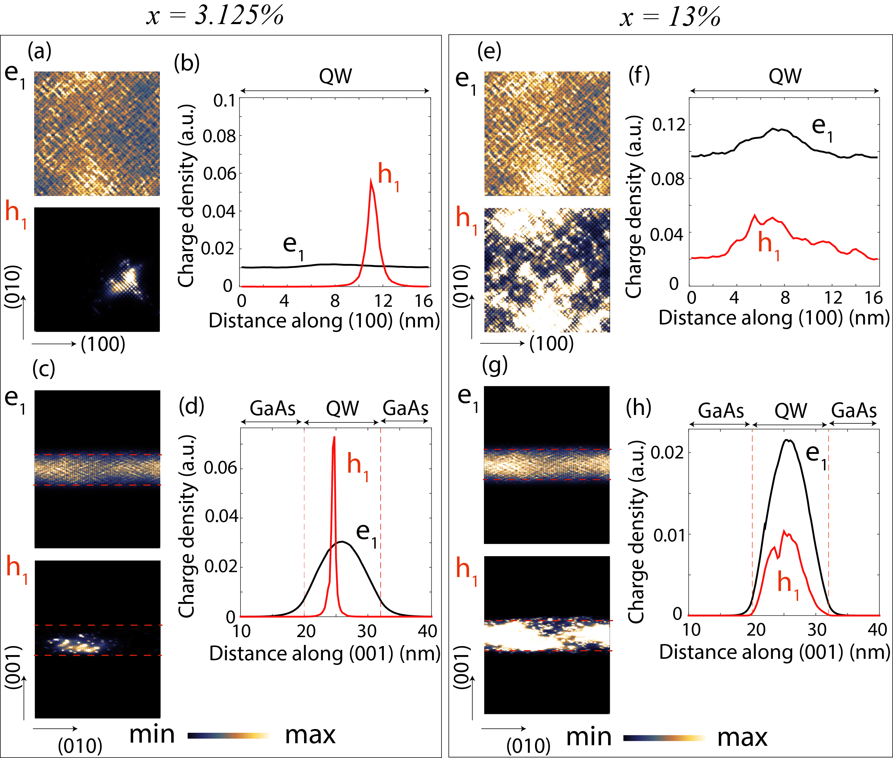
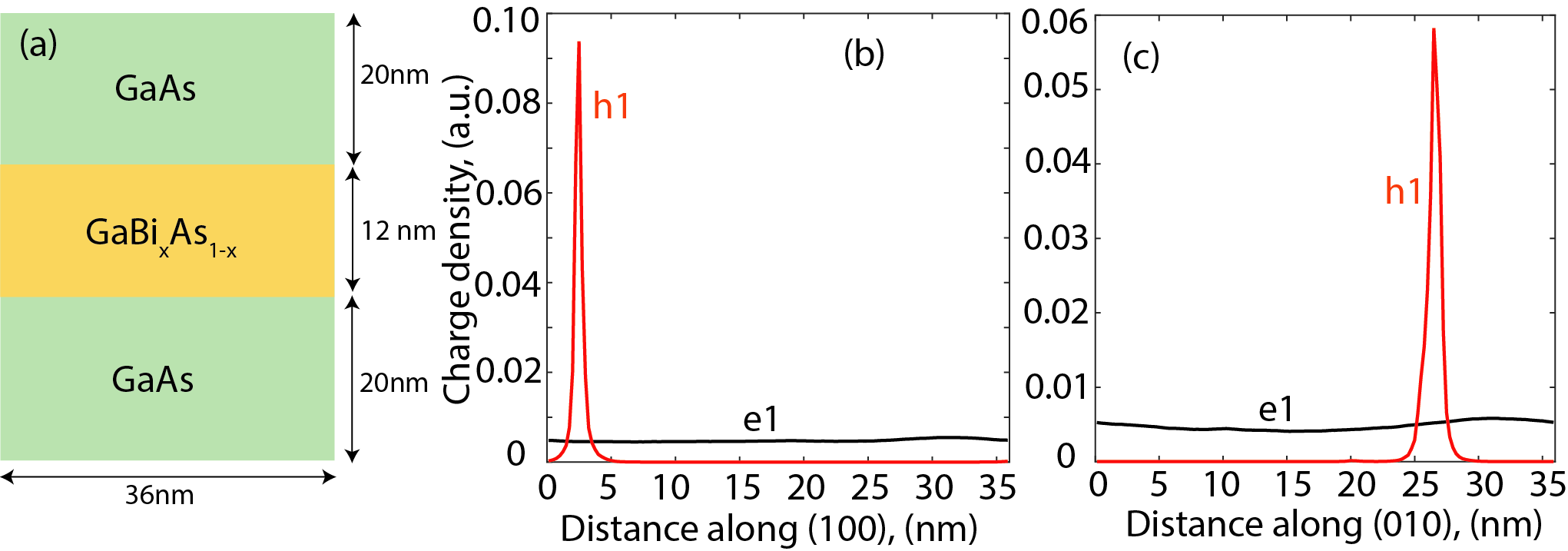
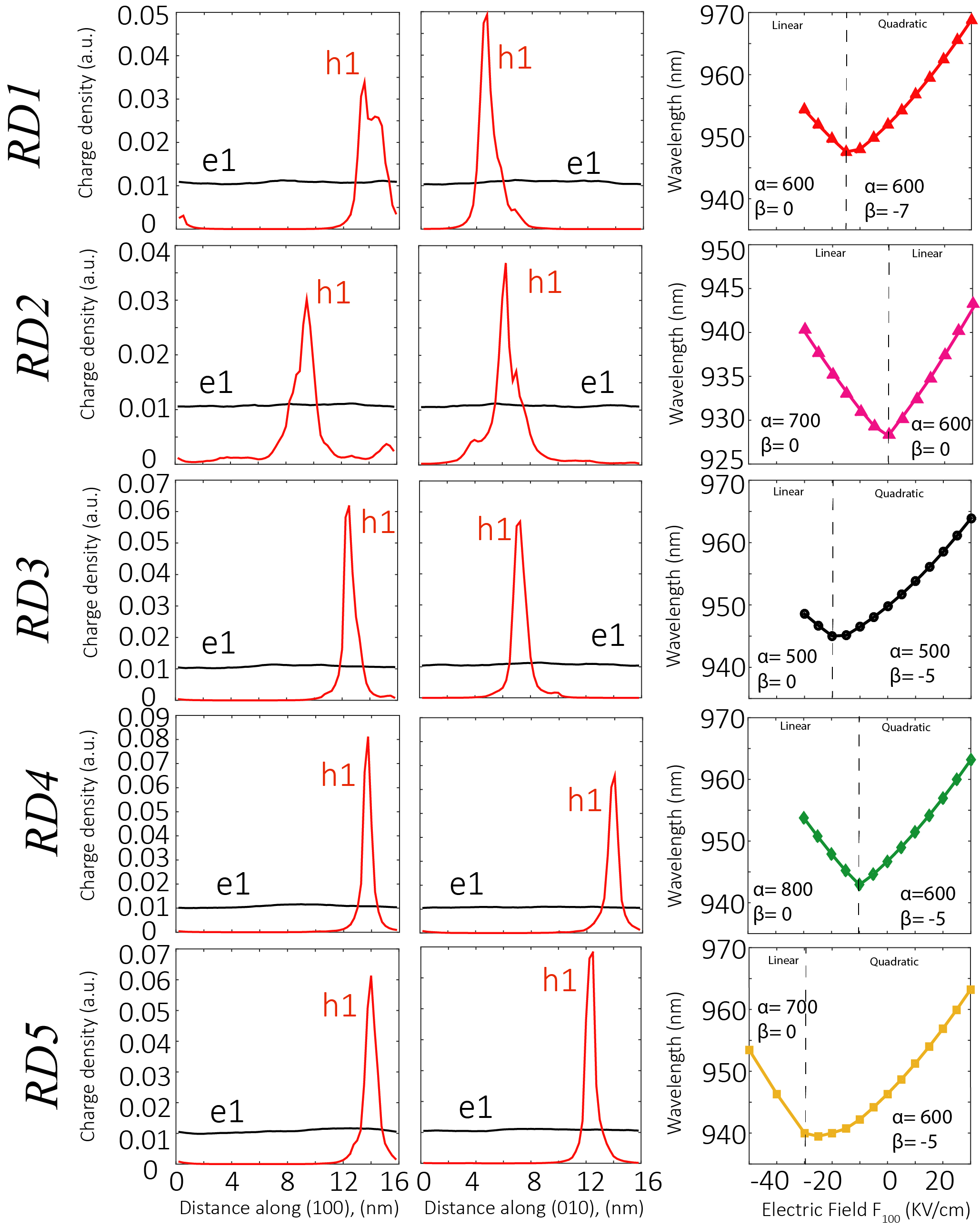
Strong Confinement of Hole Wave Functions: Let’s first look at the charge density plots for the QW with =3.125%. Fig. 3 (a) shows the 2D color plot of the electron and hole charge densities in a (001)-plane passing through the center of the QW region. The electron charge density (e1) is distributed over the whole QW region although some places of stronger confinement are visible. On the other hand, the hole charge density is very strongly confined and present only inside a small region of the QW. This is also evident from the 1D plots of the charge densities in (b). The charge density plots in other directions shown in (c) and (d) exhibit the similar nature of the confinement. The strong confinement of the hole charge density is attributed to the presence of Bi clusters Usman_PRM_2018 . It is well-established that the presence of Bi in GaAs introduces Bi related resonance states within the GaAs valence band, which interact with the valence band edge through a band anti-crossing interaction Usman_PRB_2011 . Therefore the presence of Bi clusters strongly impact the confinement of hole charge densities, whereas the electron wave functions remain relatively unperturbed and display envelope wave function character. Recent experimental measurements have provided a clear evidence for the presence of Bi clusters Wu_APL_2014 ; Puustinen_JAP_2013 . We also increased the lateral size of the QW region to 36 nm consisting of 1.33 million atoms and found the presence of similar strong confinement of the hole wave functions at =3.125% (see Fig. S3 in the supplementary material).
At the larger Bi fraction (=13%), Fig. 3 (e) shows that the electron charge density is nearly uniformly distributed over the whole QW region. However somewhat surprisingly, the hole charge density is also significantly spread with a much weaker confinement and roughly looks like the electron charge density. This is also evident from the plots of the charge density in other directions given in (f), (g), and (h) parts of Fig. 3. At =13%, the QW region consists of 12778 Bi atoms (compared to 3072 for 3.125%), therefore the overall strain in the QW region is much more uniform compared to the =3.125% case where relatively few Bi atoms implies isolated presence of Bi clusters. The charge density plots for the other two Bi fractions 6.5% and 10% are provided in the supplementary material section for reference (Fig. S4). These plots clearly exhibit a trend that the uniformity of the spatial distribution of the hole charge density increases as the Bi fraction of the QW region increases.
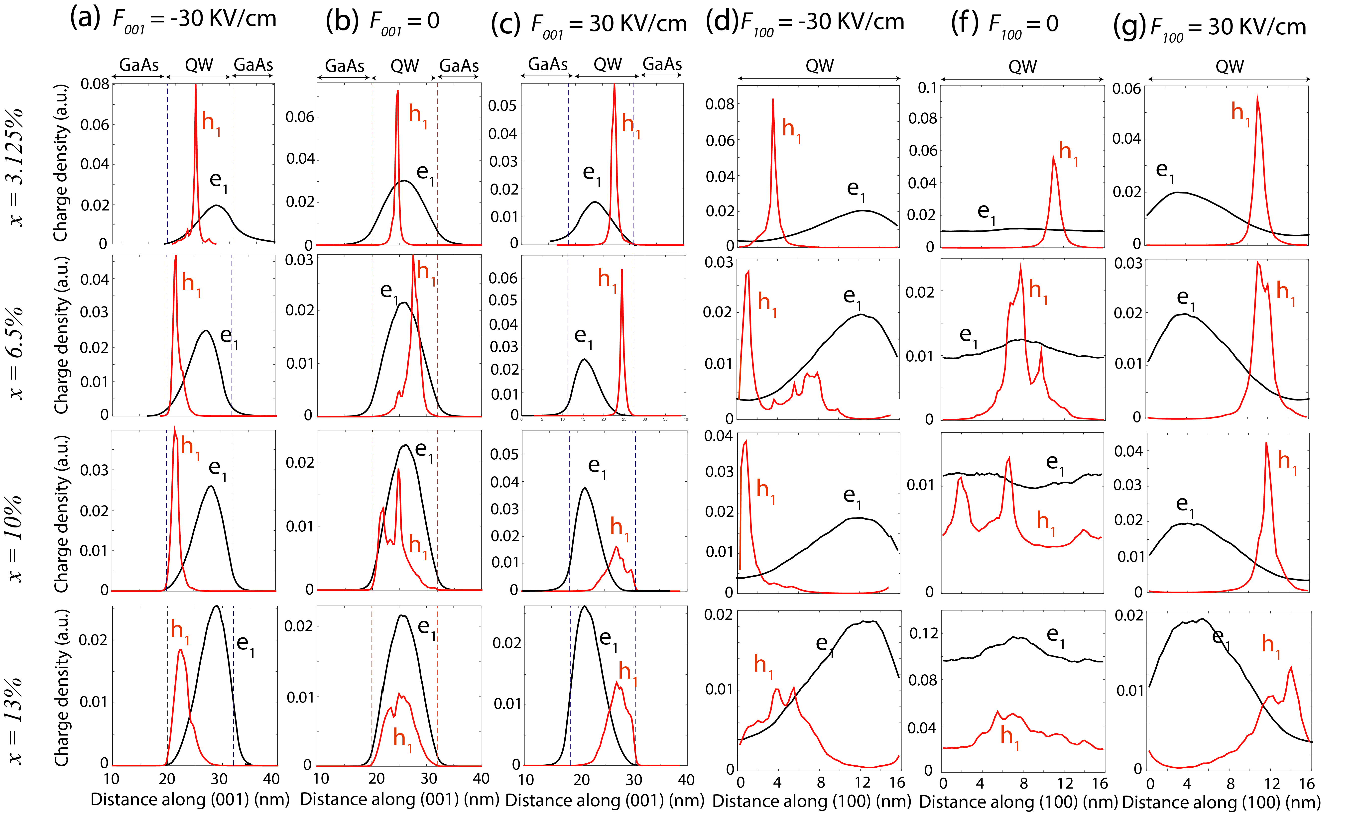
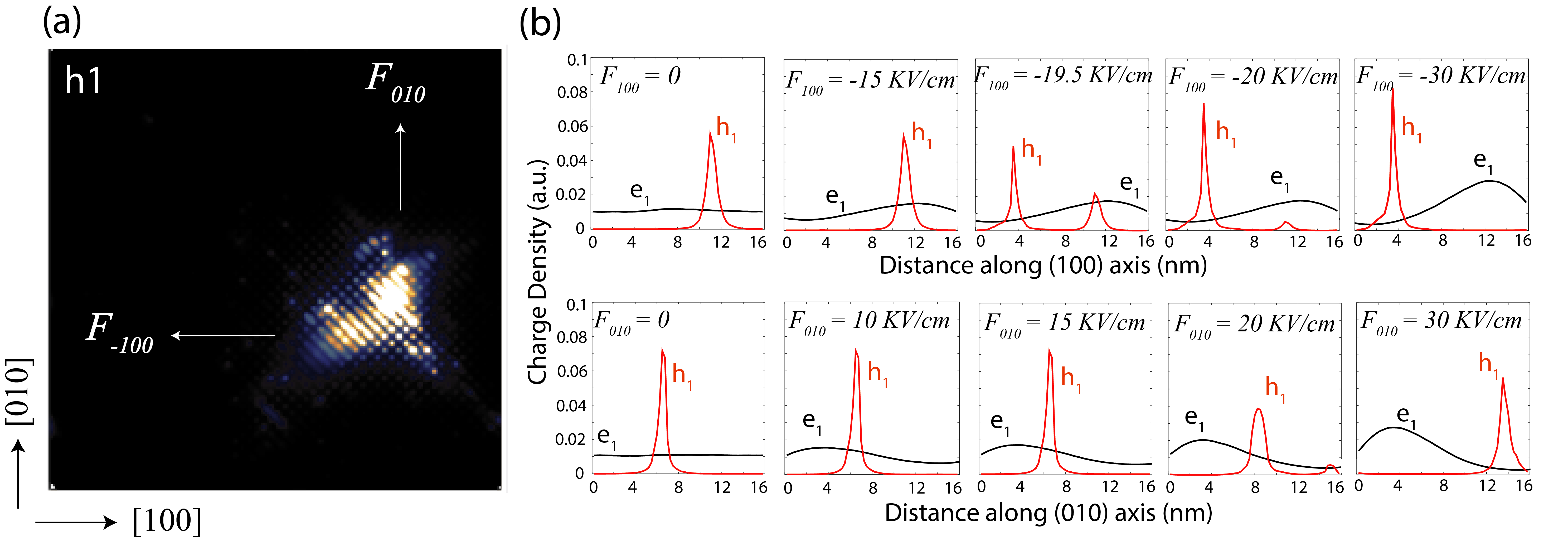
Spatial Shift of Hole Charge Density by Electric Field: The application of an electric field shifts the electron and hole wave function charge densities in the opposite directions. Ideally if the electron and hole charge densities are symmetric and uniformally distributed in the QW region, the shifts in charge densities will also be symmetric around =0. However typically even at =0, the electron and hole wave functions are separated in a nanostructure (QW or QD) due to the random alloying effect or shape asymmetry of the nanostructure Fry_PRL_2000 . This leads to inequivalent shifts in the charge densities where the electrons and holes are differently impacted by the same magnitude and direction of the electric field. Another form of asymmetry in the QCSE has been previously observed, which is linked with the preferred spatial confinement of the electron or hole wave functions that then leads to inequivalent Stark shifts of the corresponding energies depending upon the positive or negative sign of the electric fields Fry_PRL_2000 . We have provided the electric field dependent charge density plots for =6.5%, 10%, and 13% in the supplementary material (Fig. S5), which exhibit increasingly conventional shifts as increases, previously observed in many other III-V QWs studies. In Fig. 4, we only focus on =3.125% case where the hole charge density is strongly confined in a small region of the QW as shown in (a). The confinement of the hole wave functions towards the bottom right corner of the (001)-plane implies that the application of electric fields and along the (-100) and (010) directions will have to significantly displace the charge density towards the opposite edge as indicated by arrows in Fig. 4 (a).
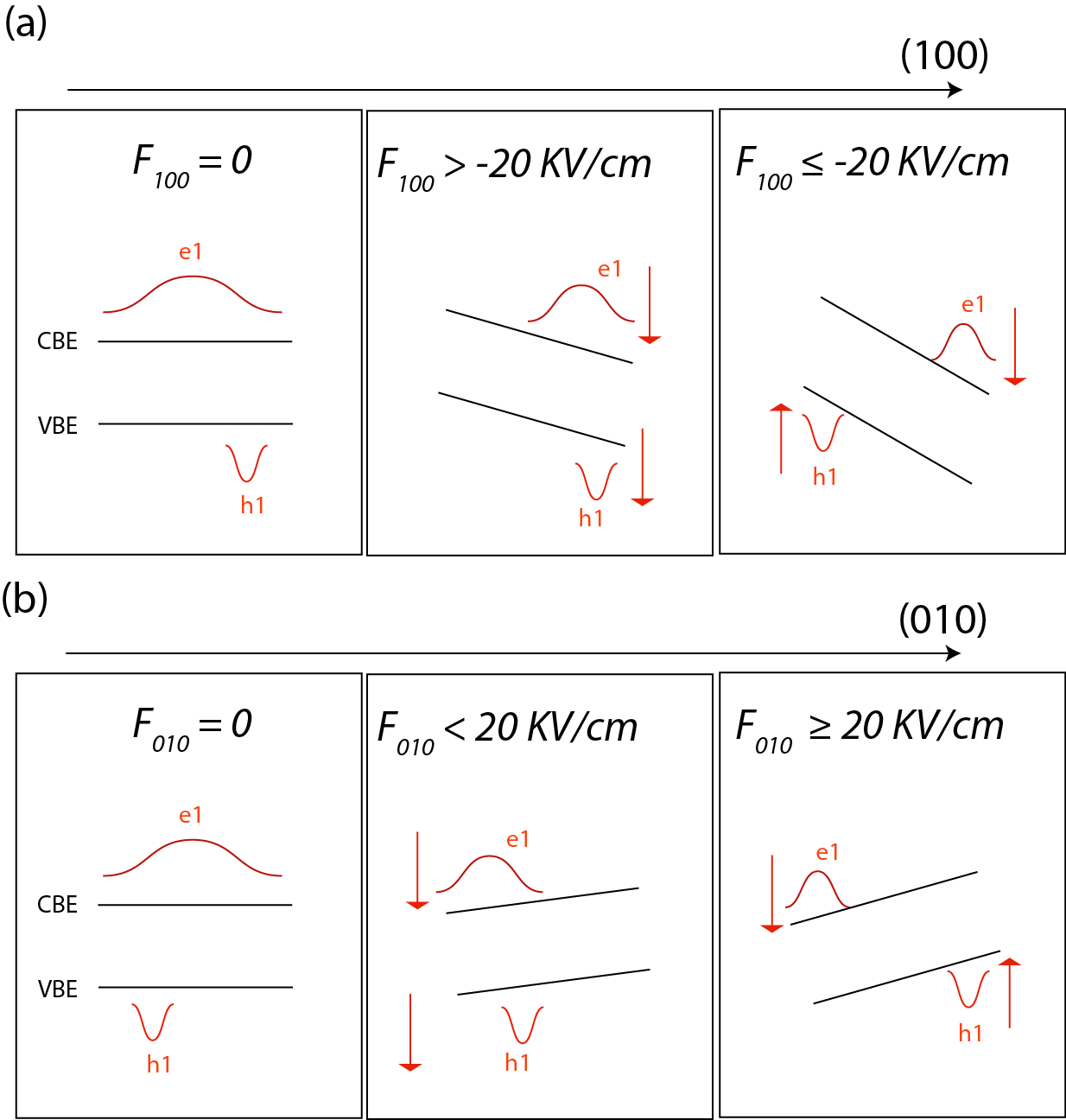
Fig.4 (b) plots the hole charge densities for various magnitudes of the and electric fields. The plots in the upper row shows that the hole wave function (h1) remains confined inside the QW region bounded by 8 nm and 12 nm along the (100) direction until is increased to 19 kV/cm. The plot of the wave function charge density at = -19.5 kV/cm shows a hybridized wave function partially confined towards the lower edge of the QW region and the remaining still confined towards the upper edge. The complete shift of the hole wave functions only occurs for -20 kV/cm. This explains the unusual Stark shifts of the hole energy (h1) plotted earlier in Fig. 2 (b). To explain it further, we have provided a schematic diagram in the supplementary material section (see Fig. S6). The application of the electric field tilts the valence band edge such that the band edge energy in the 0 8 nm region increases whereas it decreases in the region bounded by 8 16 nm, where is the distance along the (100) direction. Since for -20 40 kV/cm the hole wave function is confined in the 8 16 nm region, therefore its energy decreases. For -40 -20 kV/cm, the hole wave function shifts in the 0 8 nm region where the VBE is tilted towards higher energy, so the hole energy immediately increases with a larger slope.
The same phenomena happens when the electric field direction is along the (010) direction. As shown in the lower row of the Fig. 4(b), the hole wave function is now confined in the 0 8 nm region at zero electric field magnitude (Fig. S6). For 0, the VBE in the 0 8 nm region increases in energy and therefore the hole energy also increases. For 0, the VBE in the 0 8 nm region decreases and it increases in the 8 16 nm region. In this case, the hole wave function needs to shift from 0 8 nm to 8 16 nm region to increase its energy. However as shown in the Fig. 4(b), the hole wave function, due to its very strong confinement, remains confined in the 0 8 nm region until the electric field magnitude is increased above 20 kV/cm. Therefore the hole energy first decreases for 0 20 kV/cm and then it starts increasing for 20 40 kV/cm.
Contrarily, the electron wave function exhibits a conventional shift when the electric field is applied: it immediately shifts towards the decreasing side of conduction band edge as soon the electron field magnitude is increased above zero. Therefore the Stark shift of electron energy is quadratic for all directions of the applied electric fields. We also note that the shift in the hole energies is linear due to the stronger confinement, compared to the quadratic shift in e1 energies due to weaker confinement of the corresponding wave functions.
Effect of Random Positioning of Bi Atoms: In the above sections, we have shown that the unconventional character of the QCSE at =3.125% arise from a very strong spatial confinement of the hole wave functions, which leads to a highly asymmetric Stark shift in the valence band energies. The strong confinement of the hole wave functions, which is sensitive to the presence of Bi clusters depends on the atomic-level spatial arrangement of the Bi atoms in the QW region. In our calculations, the Bi atoms are placed randomly based on a seed value, therefore different seed values will generate different random spatial distributions of the Bi atoms in the QW region. As a result, the QW region will contain different size and types of Bi clusters. In order to investigate the effect of the spatial distributions of the Bi atoms on the QCSE, we simulated five additional random configurations of the Bi atoms labelled as to in the supplementary figure S6. For each case, we have plotted the spatial distribution of the lowest electron and the highest hole wave functions along the (100) and (010) directions and the QCSE effect for electric field. Our calculations confirm the presence of the strong confinement of the hole wave functions in all of the five different random distributions of the Bi atoms. The overall variation in the computed band-gap wavelength for the various Bi configurations is 20 nm at zero electric field, which is consistent with the published results at low Bi fraction in the QW region Usman_APL_2014 . On the other hand, as a function of the applied electric field, we find that the change in the band-gap is 30 nm. Interestingly, this change is comparable to the variation related to the alloy randomness at 3.125% Bi fraction.
The plots of the QCSE in supplementary Fig. S6 indicate that the quadratic to linear change in the wavelength dependence on the applied electric field is valid for all the investigated cases when the hole wave functions are confined close to the edges of the QW regions. For the configuration, the hole wave function (h1) exhibits a strong confinement close to the center of the QW region. In this case, our results show that the QCSE is linear for the whole range of the applied electric field, implying that the nature of QCSE (linear or quadratic) not only depends on the strong confinement of the hole wave functions but also on the relative spatial location inside the QW region. The linear QCSE for this particular case can be understood based on the presence of the hole wave function close to the centre of QW region, which implies that the application of a small non-zero electric field is sufficient to shift the hole wave function in either direction. This is the reason for the minimum value of the GSTW being at =0. Finally, we have provided the fitted values of and in Fig. S6 for all of considered random configurations. Overall the value of varied from 50010-6 eV.cm/kV to 80010-6 eV.cm/kV, and the value of varies from -510-6 (eV.cm/kV)2 to -710-6 (eV.cm/kV)2 where the QCSE is quadratic. We should point out here that these variations are computed at Bi=3.125%, for which the impact of alloy configurations is strongest. As the Bi fraction in the QW region increases, the alloy randomness effect becomes weak and therefore we expect significantly smaller variation in and at Bi=13%.
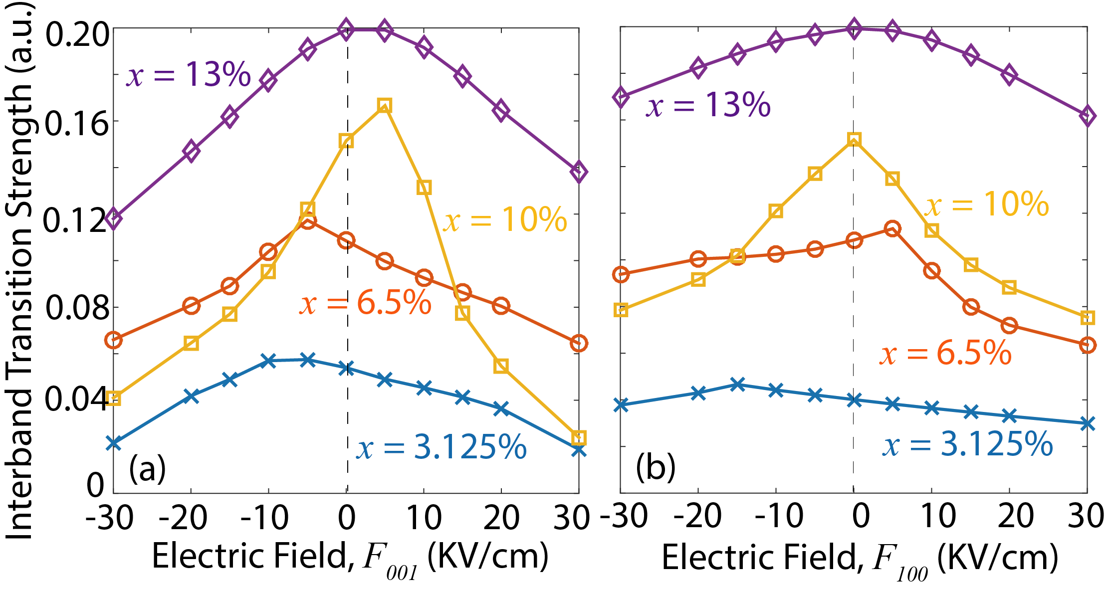
Inter-band Optical Transition Strengths: Fig. 5 plots the optical transition strengths (OTS) as a function of the applied electric fields for various Bi fractions in the QW region. The momentum matrix element between the ground electron and hole states is computed as follows Usman_PRB2_2011 :
| (4) |
where and indicates the spin up and down states, H is the tight-binding Hamiltonian in basis, and is the spatial distance between atoms and . For TE mode OTS calculation, is equal to and it is equal to for the TM mode OTS calculation. After calculting the momentun matrix elements, we compute the TE and TM mode optical transition strengths (TE100 and TM001) from Fermi’s Golden rule (by summation of the absolute values of the momentum matrix elements including spin degenerate states) Usman_PRB2_2011 :
| TE100 | (5) | ||||
| TM001 | (6) |
The OTS between the ground-state electron and hole states is strongly dependent on the overlap between the corresponding wave functions. The application of an electric field shifts the electron and hole wave functions in the opposite directions, leading to a decrease in the spatial overlap between them. This results in a decrease in the OTS magnitude as a function of the electric field. This is true for all the Bi fractions and for both electric field orientations plotted in Fig. 5. The plots also exhibit two general trends for the OTS. The first is as a function of the Bi fraction : the magnitude of the OTS increases when increases which is true for both and fields. This is because the hole wave function is highly confined at low Bi fractions and it results in lesser overlap with the relatively uniformly confined electron wave function. The second trend is related to increase in the electric field magnitude, which leads to an overall larger decrease in the OTS magnitude at higher Bi fractions when compared to the low Bi fractions. This is related to the electric field induced shift in the hole wave functions, which is stronger due to the weaker confinement level of electrons and holes. As the shift in electron wave functions is relatively similar for all , a larger decrease in the electron-hole wave function spatial overlap leads to a correspondingly larger decrease in the OTS magnitude for =10% and 13%.
4 Conclusions
Based on large-scale atomistic tight-binding simulations, we have investigated the quantum confined Stark effect (QCSE) for novel GaBixAs1-x/GaAs quantum wells. To provide a comprehensive understanding of the QCSE, we have varied the magnitude and orientation of the electric field for four different Bi compositions = 3.125%, 6.5%, 10%, 13%. Our results have revealed that at low Bi fractions (=3.125%), the character of the QCSE is dominated by the strong confinement of the hole wave functions due to the presence of Bi clusters. This leads to an unconventional nature of the QCSE. At large Bi compositions, the hole wave function confinement is weakly dictated by the presence of the Bi clusters, and therefore the QCSE exhibits a conventional quadratic dependence on the electric field irrespective of its orientations. At technologically relevant 1300 nm wavelength reported for the 13% Bi fraction, we have computed an overall shift of 22 nm in the GSTW based on a 40 kV/cm variation in the magnitude of the electric field, irrespective of its orientation. Our results document the first study of the QCSE for technologically relevant GaBixAs1-x/GaAs QWs and provide useful guidance to design optoelectronic and spintronic devices.
5 Acknowledgements
Computational resources are acknowledged from National Computational Infrastructure (NCI) under the National Computational Merit based Allocation Scheme (NCMAS).
References
- (1) Y.-H. Kuo, Y. K. Lee, Y. Ge, S. Ren, J. Roth, T. Kamins, D. B. Miller, J. S. Harris, Strong quantum-confined stark effect in germanium quantum-well structures on silicon, Nature 437 (2005) 1334.
- (2) S. Empedocles, M. Bawendi, Quantum-confined stark effect in single CdSe nanocrystallite quantum dots, Science 278 (1997) 2114.
- (3) H. Krenner, M. Sabathil, E. C. Clark, A. Kress, D. Schuh, M. Bichler, G. Abstreiter, J. J. Finley, Direct observation of controlled coupling in an individual quantum dot molecule, Phys. Rev. Lett. 94 (2005) 057402.
- (4) T. Nakaoka, S. Kako, Y. Arakawa, Unconventional quantum-confined stark effect in a single GaN quantum dot, Phys. Rev. B 73 (2006) 121305(R).
- (5) G. O. de Sousa, D. R. da Costa, A. Chaves, G. A. Farias, F. M. Peeters, Unusual quantum confined Stark effect and Aharonov-Bohm oscillations in semiconductor quantum rings with anisotropic effective masses, Phys. Rev. B 95 (2017) 205414.
- (6) H. Li, Z. Wang (Eds.), Bismuth-Containing Compounds, Springer-Verlag New York, 2013.
- (7) A. Janotti, S.-H. Wei, S. B. Zhang, Theoretical study of the effects of isovalent coalloying of Bi and N in GaAs, Phys. Rev. B 65 (2002) 115203.
- (8) Y. Zhang, A. Mascarenhas, L.-W. Wang, Similar and dissimilar aspects of IIIV semiconductors containing Bi versus N, Phys. Rev. B 71 (2005) 155201.
- (9) Z. Batool, K. Hild, T. J. C. Hosea, X. Lu, T. Tiedje, S. J. Sweeney, The electronic band structure of GaBiAs/GaAs layers: Influence of strain and band anti-crossing, J. Appl. Phys. 111 (2012) 113108.
- (10) M. Usman, C. A. Broderick, A. Lindsay, E. P. O’Reilly, Tight-binding analysis of the electronic structure of dilute bismide alloys of GaP and GaAs, Phys. Rev. B 84 (2011) 245202.
- (11) C. A. Broderick, M. Usman, S. J. Sweeney, E. P. O’Reilly, Band engineering in dilute nitride and bismide semiconductor lasers, Semicond. Sci. Technol. 27 (2012) 094011.
- (12) I. P. Marko, S. J. Sweeney, Optical and electronic processes in semiconductor materials for device applications, Springer Ser. Mater. Sci. 203 (2014) 253.
- (13) M. Usman, C. A. Broderick, Z. Batool, K. Hild, T. J. C. Hosea, S. J. Sweeney, E. P. O’Reilly, Impact of alloy disorder on the band structure of compressively strained GaBixAs1-x, Phys. Rev. B 87 (2013) 115104.
- (14) M. Usman, E. P. O’Reilly, Atomistic tight-binding study of electronic structure and interband optical transitions in GaBiAs/GaAs quantum wells, Appl. Phys. Lett. 104 (2014) 071103.
- (15) M. Usman, Large-scale atomistic simulations demonstrate dominant alloy disorder effects in GaBiAs/GaAs multiple quantum wells, Phys. Rev. Materials 2 (2018) 044602.
- (16) R. D. Richards, F. Bastiman, J. S. Roberts, R. Beanland, D. Walker, J. P. R. David, MBE grown GaAsBi/GaAs multiple quantum well structures: Structural and optical characterization, J. Cryst. Growth 425 (2015) 237–240.
- (17) M. A. G. Balanta, V. O. Gordo, A. R. H. Carvalho, J. Puustinen, H. M. Alghamdi, M. Henini, H. V. A. Galeti, M. Guina, Y. G. Gobato, Polarization resolved photoluminescence in GaAs1-xBix/GaAs quantum wells, J. of Luminescence 182 (2017) 49–52.
- (18) Y. I. Mazur, V. Dorogan, L. Dias, D. Fan, M. Schmidbauer, M. Ware, Z. Y. Zhuchenko, S. Kurlov, G. Tarasov, S.-Q. Yu, G. Marques, G. Salamo, Luminescent properties of GaAsBi/GaAs double quantum well heterostructures, J. of Luminescence 188 (2017) 209.
- (19) M. Aziz, C. Xie, V. Pusino, A. Khalida, M. Steer, I. Thayne, D. Cumming, Multispectral mid-infrared light emitting diodes on a GaAs substrate, Appl. Phys. Lett. 111 (2017) 102102.
- (20) H. Makhloufi, P. Boonpeng, S. M. adn J. Nicolai adn A. Arnoult, T. Hungria, G. L. adn C. Gatel, A. Ponchet, H. Carrere, X. Marie, C. Fontaine, Molecular beam epitaxy and properties of GaAsBi/GaAs quantum wells grown by molecular beam epitaxy: effect of thermal annealing, Nanoscale Research Lett. 9 (2014) 123.
- (21) I. P. Marko, C. A. Broderick, S. R. Jin, P. Ludewig, W. Stolz, K. Volz, J. M. Rorison, E. P. O’Reilly, S. J. Sweeney, Optical gain in GaAsBi/GaAs quantum well diode lasers, Sci. Rep. 6 (2016) 28863.
- (22) M. Balanta, J. Kopaczek, V. Gordo, B. Santos, A. Rodrigues, H. Galeti, R. Richards, F. Bastiman, J. David, R. Kudrawiec, Y. Gobato, Optical and spin properties of localized and free excitons in GaBixAs1-x/GaAs multiple quantum wells, J. Phys. D: Appl. Phys. 49 (2016) 355104.
- (23) P. Patil, E. Luna, T. Matsuda, K. Yamada, K. Kamiya, F. Ishikawa, S. Shimomura, GaAsBi/GaAs multi-quantum well LED grown by molecular beam epitaxy using a two-substrate-temperature technique, Nanotechnology 28 (2017) 105702.
- (24) M. Usman, C. A. Broderick, E. P. O’Reilly, Impact of disorder on the optoelectronic properties of GaNyAs1-x-yBix alloys and heterostructures, Phys. Rev. Applied 10 (2018) 044024.
- (25) S. Mazzucato, T. T. Zhang, H. Carrère, D. Lagarde, P. Boonpeng, A. Arnoult, G. Lacoste, A. Balocchi, T. Amand, C. Fontaine, X. Marie, Electron spin dynamics and g-factor in GaAsBi, Applied Physics Letters 102 (2013) 252107.
- (26) P. N. Keating, Effect of invariance requirements on the elastic strain energy of crystals with application to the diamond structure, Phys. Rev. 145 (1966) 637.
- (27) G. Klimeck, R. Bowen, T. Boykin, C. Lazaro, T. Cwik, A. Stoica, Si tight-binding parameters from genetic algorithm fitting, Superlattices and Microstructures 27 (2000) 519.
- (28) A. Sawamura, J. Otsuka, T. Kato, T. Kotani, S. Souma, Nearest-neighbor sp3d5s∗ tight-binding parameters based on the hybrid quasi-particle self-consistent GW method verified by modeling of type-II superlattices, Optical Materials Express 8 (2018) 1569.
- (29) C. A. Broderick, S. Mazzucato, H. Carrère, T. Amand, H. Makhloufi, A. Arnoult, C. Fontaine, O. Donmez, A. Erol, M. Usman, E. P. O’Reilly, X. Marie, Anisotropic electron g factor as a probe of the electronic structure of GaBixAs1-x/GaAs epilayers, Phys. Rev. B 90 (2014) 195301.
- (30) C. A. Broderick, P. E. Harnedy, P. Ludewig, Z. L. Bushell, K. Volz, R. J. Manning, E. P. O’Reilly, Determination of type-I band offsets in GaBixAs1-x quantum wells using polarisation-resolved photovoltage measurements and 12-band kp calculations, Semicond. Sci. Technol. 30 (2015) 094009.
- (31) O. Donmez, A. Erol, M. Arikan, H. Makhloufi, A. Arnoult, C. Fontaine, Semicond. Sci. Technol. 30 (2015) 094016.
- (32) B. Zhang, W.-Y. Qiu, P.-P. Chen, X.-J. Wang, J. Appl. Phys. 123 (2018) 035702.
- (33) F. Dybala, J. Kopaczek, M. Gladysiewicz, E.-M. Pavelescu, C. Romanitan, O. Ligor, A. Arnoult, C. Fontaine, R. Kudrawiec, J. of Appl. Phys. 111 (2017) 192104.
- (34) K. Collar, J. Li, W. Jiao, Y. Guan, M. Losurdo, J. Humlicek, A. S. Brown, AIP Advances 7 (2017) 075016.
- (35) R. Kudrawiec, J. Kopaczek, M. Polak, P. Scharoch, M. Gladysiewicz, J. Misiewicz, R. Richards, F. Bastiman, J. David, J. Appl. Phys. 116 (2014) 233508.
- (36) M. P. Polak, P. Scharoch, R. Kudrawiec, Semicond. Sci. Technol. 30 (2015) 094001.
- (37) L. C. Bannow, O. Rubel, S. Badescu, P. Rosenow, J. Hader, J. Moloney, R. Tonner, S. Koch, Phys. Rev. B 93 (2016) 205202.
- (38) G. Klimeck, S. S. Ahmed, N. Kharche, M. Korkusinski, M. Usman, M. Prada, T. Boykin, Atomistic simulation of realistically sized nanodevices using NEMO 3-D – part I: applications, IEEE Trans. Electron. Dev. 54 (2007) 2090.
- (39) M. Usman, Y. M. Tan, H. Ryu, S. Ahmed, H. Krenner, T. Boykin, G. Klimeck, Quantitative excited state spectroscopy of a single ingaas quantum dot molecule through multi-million-atom electronic structure calculations, Nanotechnology 22 (2011) 315709.
- (40) D. Miller, D. Chemla, T. Damen, A. Gossard, W. Wiegmann, T. Wood, C. Burrus, Band-Edge Electroabsorption in Quantum Well Structures: The Quantum-Confined Stark Effect, Phys. Rev. Lett. 53 (1984) 2173.
- (41) D. Miller, D. Chemla, T. Damen, A. Gossard, W. Wiegmann, T. Wood, C. Burrus, Electric field dependence of optical absorption near the band gap of quantum-well structures, Phys. Rev. B 32 (1985) 1043.
- (42) G. lengyel, K. Jelley, R. Engelmann, A semi-empirical model for electroabsorption in GaAs/AlGaAs multiple quantum well modulator structures, IEEE Journal of Quantum Electronics 26 (1990) 296.
- (43) W. Sukkabot, Atomistic tight-binding computations of the structural and optical properties of CdTe/CdX (X=S and Se)/ZnS core/shell/shell nanocrystals, Philosophical Magazine 98 (2018) 1360.
- (44) J. Robinson, J. Rice, K. Lee, J. Na, R. Taylora, Quantum-confined Stark effect in a single InGaN quantum dot under a lateral electric field, Appl. Phys. Lett. 86 (2005) 213103.
- (45) J. Seufert, M. Obert, M. Scheibner, N. Gippius, G. Bacher, A. Forchel, Stark effect and polarizability in a single CdSe/ZnSe quantum dot, Appl. Phys. Lett. 79 (2001) 1033.
- (46) S. J. Sweeney, S. R. Jin, Bismide-nitride alloys: promising for efficient light emitting devices in the near- and mid-infrared, J. Appl. Phys. 113 (2013) 043110.
- (47) M. Wu, E. Luna, J. Puustinen, M. Guina, A. Trampert, Formation and phase transformation of Bi-containing QD-like clusters in annealed GaAsBi, Appl. Phys. Lett. 105 (2014) 041602.
- (48) J. Puustinen, M. Wu, E. Luna, A. Schramm, P. Laukkanen, M. Laitinen, T. Sajavaara, M. Guina, Variation of lattice constant and cluster formation in GaAsBi, J. Appl. Phys. 114 (2013) 243504.
- (49) P. F. PW, I. E. Itskevich, D. J. Mowbray, M. Skolnick, J. F. JJ, J. Barker, E. O’Reilly, L. Wilson, I. Larkin, P. Maksym, M. Hopkinson, M. Al-Khafaji, J. David, A. Cullis, G. Hill, J. Clark, Inverted electron-hole alignment in InAs-GaAs self-assembled quantum dots, Phys. Rev. Lett. 84 (2000) 733.
- (50) M. Usman, T. Inoue, Y. Harda, G. Klimeck, T. Kita, Experimental and atomistic theoretical study of degree of polarization from multilayer inas/gaas quantum dot stacks, Phys. Rev. B 84 (2011) 115321.
Supplementary Figures
